June 2001
1
MIC39150/39151
MIC39150/39151
Micrel
MIC39150/39151
1.5A Low-Voltage Low-Dropout Regulator
Final Information
General Description
The MIC39150 and MIC39151 are 1.5A low-dropout linear
voltage regulators that provide a low voltage, high current
output with a minimum of external components. Utilizing
Micrel's proprietary Super
eta PNPTM pass element, the
MIC39150/1 offers extremely low dropout (typically 375mV at
1.5A) and low ground current (typically 17mA at 1.5A).
The MIC39150/1 is ideal for PC add-in cards that need to
convert from 3.3V to 2.5V or 2.5V to 1.8V. A guaranteed
maximum dropout voltage of 500mV over all operating con-
ditions allows the MIC39150/1 to provide 2.5V from a supply
as low as 3V or 1.8V from a supply as low as 2.3V. The
MIC39150/1 also has fast transient response for heavy
switching applications. This device requires only 10
µ
F of
output capacitance to maintain stability and achieve fast
transient response
The MIC39150/1 is fully protected with overcurrent limiting,
thermal shutdown, reversed-battery protection, reversed-
lead insertion, and reverse-leakage protection. The MIC39151
offers a TTL-logic compatible enable pin and an error flag that
indicates undervoltage and over current conditions. Offered
in fixed voltages of 2.5V, 1.8V and 1.65V, the MIC39150/1
comes in the TO-220 and TO-263 packages and is an ideal
upgrade to older, NPN-based linear voltage regulators.
For applications requiring input voltage greater than 16V or
automotive load dump protection, see the MIC29150/1/2/3
family.
Features
∑ 1.5A minimum guaranteed output current
∑ 500mV maximum dropout voltage over temperature
Ideal for 3.0V to 2.5V conversion
Ideal for 2.5 to 1.8V or 1.65V conversion
∑ 1% initial accuracy
∑ Low ground current
∑ Current limiting and Thermal shutdown
∑ Reversed-battery and reversed lead insertion protection
∑ Reversed-leakage protection
∑ Fast transient response
∑ TO-263 and TO-220 packaging
∑ TTL/CMOS compatible enable pin (MIC39151 only)
∑ Error flag output (MIC39151 only)
Applications
∑ Low-voltage digital ICs
∑ LDO linear regulator for PC add-in cards
∑ High-efficiency linear power supplies
∑ SMPS post regulator
∑ Low-voltage microcontrollers
∑ StrongARMTM processor supply
Micrel, Inc. ∑ 1849 Fortune Drive ∑ San Jose, CA 95131 ∑ USA ∑ tel + 1 (408) 944-0800 ∑ fax + 1 (408) 944-0970 ∑ http://www.micrel.com
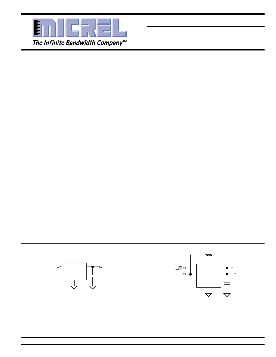
Typical Application
MIC39150-2.5
IN
OUT
GND
10µF
tantalum
V
IN
3.3V
V
OUT
2.5V
MIC39150
MIC39151-2.5
IN
OUT
GND
10µF
tantalum
V
IN
3.3V
V
OUT
2.5V
EN
FLG
ERROR FLAG
OUTPUT
ENABLE
SHUTDOWN
100k
MIC39151
StrongARM is a trademark of Advanced RSIC Machines, Ltd.
MIC39150/39151
Micrel
MIC39150/39151
2
June 2001
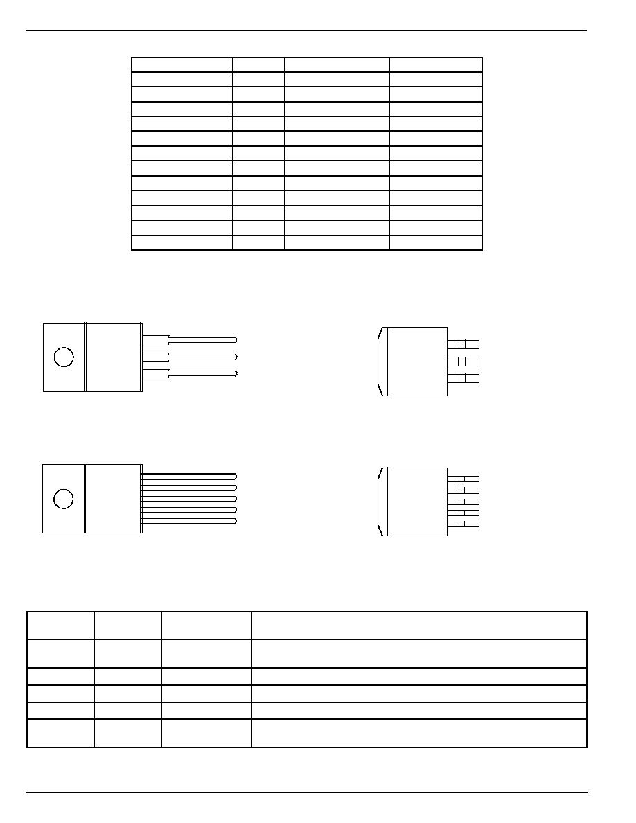
Pin Description
Pin Number
Pin Number
Pin Name
Pin Function
MIC39150
MIC39151
1
EN
Enable (Input): TTL/CMOS compatible input. Logic high = enable; logic low
or open = shutdown
1
2
IN
Unregulated Input: +16V maximum supply.
2,
TAB
3,
TAB
GND
Ground: Ground pin and
TAB
are internally connected.
3
4
OUT
Regulator Output
5
FLG
Error Flag (Ouput): Open-collector output. Active low indicates an output
fault condition.
Pin Configuration
TAB
3
OUT
2
GND
1
IN
MIC39150-x.xBT
TO-220-3 (T)
TAB
5
FLG
4
OUT
3
GND
2
IN
1
EN
MIC39151-x.xBT
TO-220-5 (T)
TAB
3
OUT
2
GND
1
IN
MIC39150-x.xBU
TO-263-3 (U)
TAB
5
FLG
4
OUT
3
GND
2
IN
1
EN
MIC39151-x.xBU
TO-263-5 (U)
Ordering Information
Part Number
Voltage
Temperature Range
Package
MIC39150-1.65BT
1.65V
≠40
∞
C to +125
∞
C
3-lead TO-220
MIC39150-1.65BU
1.65V
≠40
∞
C to +125
∞
C
3-lead TO-263
MIC39151-1.65BT
1.65V
≠40
∞
C to +125
∞
C
5-lead TO-220
MIC39151-1.65BU
1.65V
≠40
∞
C to +125
∞
C
5-lead TO-263
MIC39150-1.8BT
1.8V
≠40
∞
C to +125
∞
C
3-lead TO-220
MIC39150-1.8BU
1.8V
≠40
∞
C to +125
∞
C
3-lead TO-263
MIC39151-1.8BT
1.8V
≠40
∞
C to +125
∞
C
5-lead TO-220
MIC39151-1.8BU
1.8V
≠40
∞
C to +125
∞
C
5-lead TO-263
MIC39150-2.5BT
2.5V
≠40
∞
C to +125
∞
C
3-lead TO-220
MIC39150-2.5BU
2.5V
≠40
∞
C to +125
∞
C
3-lead TO-263
MIC39151-2.5BT
2.5V
≠40
∞
C to +125
∞
C
5-lead TO-220
MIC39151-2.5BU
2.5V
≠40
∞
C to +125
∞
C
5-lead TO-263
June 2001
3
MIC39150/39151
MIC39150/39151
Micrel
Electrical Characteristics
V
IN
= V
OUT
+1V; V
EN
= 2.4V; T
J
= 25
∞
C, bold values indicate ≠40
∞
C
T
J
+125
∞
C; unless noted
Symbol
Parameter
Condition
Min
Typ
Max
Units
V
OUT
Output Voltage
10mA
≠1
1
%
10mA
I
OUT
1.5A, V
OUT
+ 1V
V
IN
8V
≠2
2
%
Line Regulation
I
OUT
= 10mA, V
OUT
+ 1V
V
IN
16V
0.06
0.5
%
Load Regulation
V
IN
= V
OUT
+ 1V, 10mA
I
OUT
1.5A,
0.2
1
%
V
OUT
/
T
Output Voltage Temp. Coefficient,
20
100
ppm/
∞
C
Note 5
V
DO
Dropout Voltage, Note 6
I
OUT
= 100mA,
V
OUT
= ≠1%
80
200
mV
I
OUT
= 750mA,
V
OUT
= ≠1%
260
mV
I
OUT
= 1.5A,
V
OUT
= ≠1%
375
500
mV
I
GND
Ground Current, Note 7
I
OUT
= 750mA, V
IN
= V
OUT
+ 1V
4
20
mA
I
OUT
= 1.5A, V
IN
= V
OUT
+ 1V
17
mA
I
GND(do)
Dropout Ground Pin Current
V
IN
V
OUT(nominal)
≠ 0.5V, I
OUT
= 10mA
1.1
mA
I
OUT(lim)
Current Limit
V
OUT
= 0V, V
IN
= V
OUT
+ 1V
2.8
A
I
OUT(min)
Minimum Load Current
7
10
mA
Enable Input (MIC39151)
V
EN
Enable Input Voltage
logic low (off)
0.8
V
logic high (on)
2.25
V
I
IN
Enable Input Current
V
EN
= 2.25V
1
15
30
µ
A
75
µ
A
V
EN
= 0.8V
2
µ
A
4
µ
A
I
OUT(shdn)
Shutdown Output Current
Note 8
10
20
µ
A
Flag Output (MIC39151)
I
FLG(leak)
Output Leakage Current
V
OH
= 16V
0.01
1
µ
A
2
µ
A
V
FLG(do)
Output Low Voltage
V
IN
= 2.250V, I
OL
, = 250
µ
A, Note 9
180
300
mV
400
mV
V
FLG
Low Threshold
% of V
OUT
93
%
High Threshold
% of V
OUT
99.2
%
Hysteresis
1
%
Absolute Maximum Ratings
(Note 1)
Supply Voltage (V
IN
) ..................................... ≠20V to +20V
Enable Voltage (V
EN
) .................................................. +20V
Storage Temperature (T
S
) ....................... ≠65
∞
C to +150
∞
C
Lead Temperature (soldering, 5 sec.) ....................... 260
∞
C
ESD, Note 3
Operating Ratings
(Note 2)
Supply Voltage (V
IN
) .................................. +2.25V to +16V
Enable Voltage (V
EN
) .................................................. +16V
Maximum Power Dissipation (P
D(max)
) ..................... Note 4
Junction Temperature (T
J
) ....................... ≠40
∞
C to +125
∞
C
Package Thermal Resistance
TO-263
(
JC
) ......................................................... 2
∞
C/W
TO-220 (
JC
) ......................................................... 2
∞
C/W

MIC39150/39151
Micrel
MIC39150/39151
4
June 2001
Note 1.
Exceeding the absolute maximum ratings June damage the device.
Note 2.
The device is not guaranteed to function outside its operating rating.
Note 3.
Devices are ESD sensitive. Handling precautions recommended.
Note 4.
P
D(max)
= (T
J(max)
≠ T
A
)
˜
JA
, where
JA
depends upon the printed circuit layout. See "Applications Information."
Note 5.
Output voltage temperature coefficient is
V
OUT(worst case)
˜
(T
J(max)
≠ T
J(min)
) where T
J(max)
is +125
∞
C and T
J(min)
is ≠40
∞
C.
Note 6.
V
DO
= V
IN
≠ V
OUT
when V
OUT
decreases to 98% of its nominal output voltage with V
IN
= V
OUT
+ 1V. For output voltages below 2.25V, dropout
voltage is the input-to-output voltage differential with the minimum input voltage being 2.25V. Minimum input operating voltage is 2.25V.
Note 7.
I
GND
is the quiescent current. I
IN
= I
GND
+ I
OUT
.
Note 8.
V
EN
0.8V, V
IN
8V, and V
OUT
= 0V.
Note 9.
For a 2.5V device, V
IN
= 2.250V (device is in dropout).
June 2001
5
MIC39150/39151
MIC39150/39151
Micrel
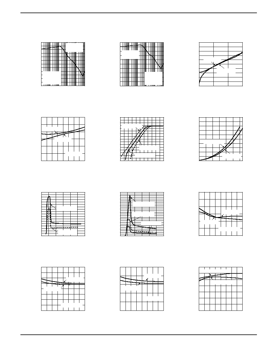
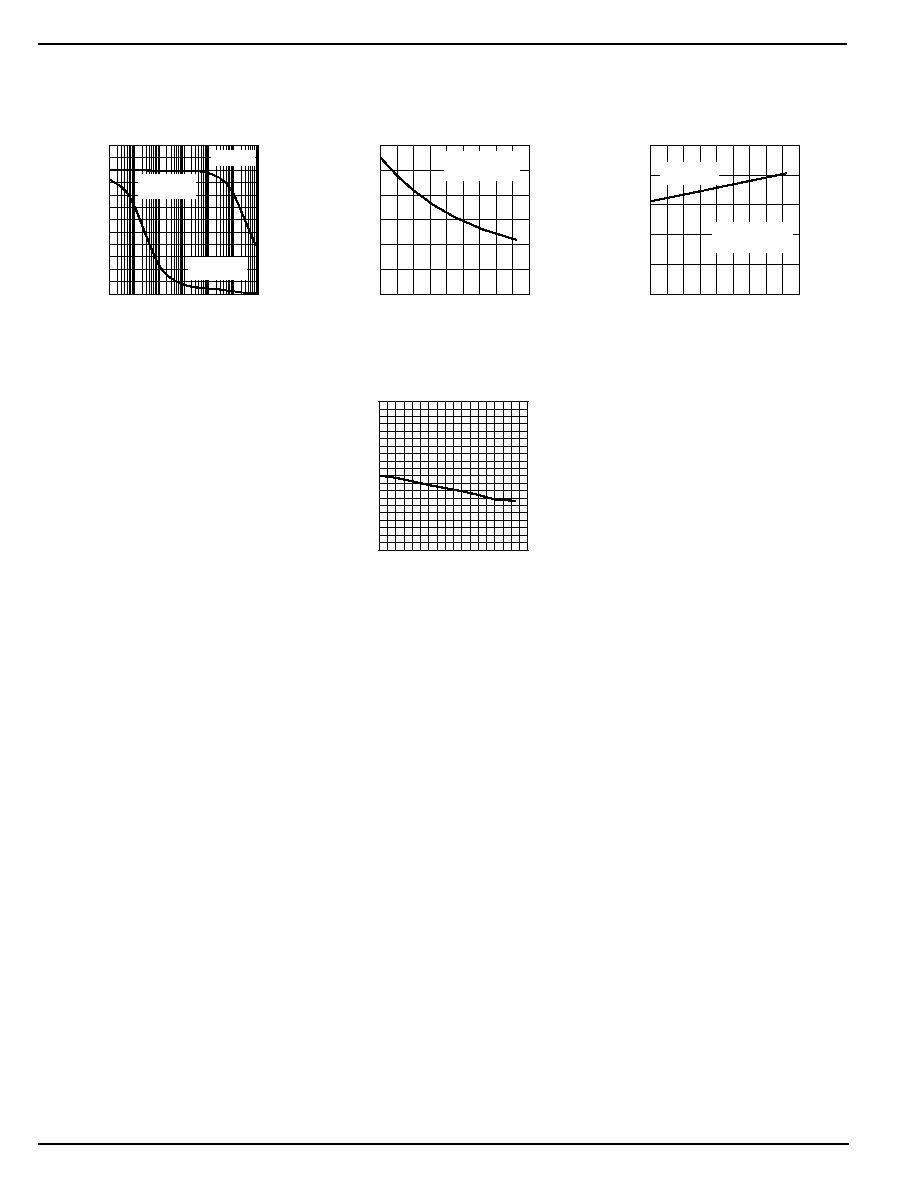
Typical Characteristics
0
10
20
30
40
50
60
1E+1 1E+2 1E+3 1E+4 1E+5 1E+6
PSRR (dB)
FREQUENCY (Hz)
Power Supply
Rejection Ratio
I
LOAD
= 1.5A
C
OUT
= 10
µ
F
C
IN
= 0
V
IN
= 3.3V
V
OUT
= 2.5V
10
100
1k
10k
100k
1M
0
10
20
30
40
50
1E+1 1E+2 1E+3 1E+4 1E+5 1E+6
PSRR (dB)
FREQUENCY (Hz)
Power Supply
Rejection Ratio
I
LOAD
= 1.5A
C
OUT
= 47
µ
F
C
IN
= 0
V
IN
= 3.3V
V
OUT
= 2.5V
10
100
1k
10k
100k
1M
0
100
200
300
400
500
0
500
1000
1500
DROPOUT VOLTAGE (mV)
OUTPUT CURRENT (mA)
Dropout Voltage
vs. Output Current
V
OUT
= 2.5V
V
OUT
= 1.8V
0
100
200
300
400
500
600
-40 -20 0
20 40 60 80 100 120
DROPOUT VOLTAGE (mV)
TEMPERATURE (
∞
C)
Dropout Voltage
vs. Temperature
I
LOAD
= 1.5A
V
OUT
= 2.5V
V
OUT
= 1.8V
1.2
1.4
1.6
1.8
2.0
2.2
2.4
2.6
2.8
1.4
1.6
1.8
2
2.2
2.4
2.6
2.8
3
3.2
3.4
3.6
OUTPUT VOLTAGE (V)
INPUT VOLTAGE (V)
Dropout Characteristics
I
LOAD
= 100mA
I
LOAD
= 750mA
I
LOAD
= 1.5A
0
5
10
15
20
25
0
250 500 750 1000 1250 1500
GROUND CURRENT (mA)
OUTPUT CURRENT (mA)
Ground Current
vs. Output Current
V
OUT
= 2.5V
V
OUT
= 1.8V
0.0
0.2
0.4
0.6
0.8
1.0
1.2
1.4
1.6
1.8
0
2
4
6
8
10
12
GROUND CURRENT (mA)
SUPPLY VOLTAGE (V)
Ground Current
vs. Supply Voltage
I
LOAD
= 10mA
I
LOAD
= 100mA
0
5
10
15
20
25
30
35
40
45
50
55
60
65
0
2
4
6
8
10
12
GROUND CURRENT (mA)
SUPPLY VOLTAGE (V)
Ground Current
vs. Supply Voltage
I
LOAD
= 750mA
I
LOAD
= 1500mA
I
LOAD
= 1000mA
0.30
0.31
0.32
0.33
0.34
0.35
0.36
-40 -20 0
20 40 60 80 100 120
GROUND CURRENT (mA)
TEMPERATURE (
∞
C)
Ground Current
vs. Temperature
I
LOAD
= 10mA
V
OUT
= 2.5V
V
OUT
= 1.8V
0
1
2
3
4
5
6
7
8
-40 -20 0
20 40 60 80 100 120
GROUND CURRENT (mA)
TEMPERATURE (
∞
C)
Ground Current
vs. Temperature
I
LOAD
= 750mA
V
OUT
= 1.8V
V
OUT
= 2.5V
0
5
10
15
20
25
-40 -20 0
20 40 60 80 100 120
GROUND CURRENT (mA)
TEMPERATURE (
∞
C)
Ground Current
vs. Temperature
I
LOAD
= 1.5A
V
OUT
= 1.8V
V
OUT
= 2.5V
0
0.5
1.0
1.5
2.0
2.5
3.0
3.5
-40 -20 0
20 40 60 80 100 120
SHORT CIRCUIT CURRENT (A)
TEMPERATURE (
∞
C)
Short Circuit vs.
Temperature
typical 1.8V device
typical 2.5V device
MIC39150/39151
Micrel
MIC39150/39151
6
June 2001
0
1
2
3
4
5
6
0.01 0.1
1
10
100 100010000
FLAG VOLTAGE (V)
RESISTANCE (k
)
Error Flag
Pull-Up Resistor
V
IN
= 5V
FLAG HIGH
(OK)
FLAG LOW
(FAULT)
0
2
4
6
8
10
12
-40 -20 0 20 40 60 80 100120140
ENABLE CURRENT
µ
A)
TEMPERATURE (
∞
C)
Enable Current
vs. Temperature
V
IN
= V
OUT
+ 1V
V
EN
= 2.4V
0
50
100
150
200
250
-40 -20 0 20 40 60 80 100120140
FLAG VOLTAGE (mV)
TEMPERATURE (
∞
C)
Flag-Low Voltage
vs. Temperature
V
IN
= 2.25V
R
PULL-UP
= 22k
FLAG-LOW
VOLTAGE
1.60
1.61
1.62
1.63
1.64
1.65
1.66
1.67
1.68
1.69
1.70
-40 -20 0 20 40 60 80 100120140
OUTPUT VOLTAGE (V)
TEMPERATURE (
∞
C)
Output Voltage vs.
Temperature
June 2001
7
MIC39150/39151
MIC39150/39151
Micrel
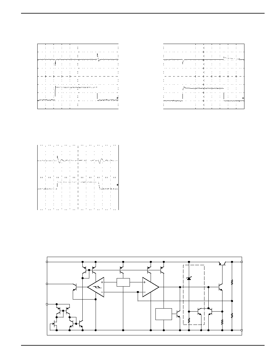
Functional Diagram
Ref.
18V
O.V.
I
LIMIT
Thermal
Shut-
down
1.240V
1.180V
EN*
IN
FLAG*
GND
OUT
* MIC39151 only
Functional Characteristics
Load Transient Response
TIME (250
µ
s/div.)
LO
AD CURRENT
(500mA/div
.
)
OUTPUT V
O
L
T
A
G
E
(500mV/div
.
)
V
IN
= 3.3V
V
OUT
= 2.5V
C
OUT
= 10
µ
F
1.5A
100mA
Load Transient Response
TIME (250
µ
s/div.)
LO
AD CURRENT
(500mA/div
.
)
OUTPUT V
O
L
T
A
G
E
(500mV/div
.
)
V
IN
= 3.3V
V
OUT
= 2.5V
C
OUT
= 47
µ
F
1.5A
10mA
Line Transient Response
TIME (500
µ
s/div.)
INPUT V
O
L
T
A
G
E
(2V/div
.
)
OUTPUT V
O
L
T
A
G
E
(50mV/div
.
)
V
OUT
= 2.5V
C
OUT
= 10
µ
F
I
LOAD
= 10mA
5V
3.3V
MIC39150/39151
Micrel
MIC39150/39151
8
June 2001
Applications Information
The MIC39150/1 is a high-performance low-dropout voltage
regulator suitable for moderate to high-current voltage regu-
lator applications. Its 500mV dropout voltage at full load and
overtemperature makes it especially valuable in battery-
powered systems and as high-efficiency noise filters in post-
regulator applications. Unlike older NPN-pass transistor de-
signs, where the minimum dropout voltage is limited by the
base-to-emitter voltage drop and collector-to-emitter satura-
tion voltage, dropout performance of the PNP output of these
devices is limited only by the low V
CE
saturation voltage.
A trade-off for the low dropout voltage is a varying base drive
requirement. Micrel's Super
eta PNPTM process reduces
this drive requirement to only 2% to 5% of the load current.
The MIC39150/1 regulator is fully protected from damage
due to fault conditions. Current limiting is provided. This
limiting is linear; output current during overload conditions is
constant. Thermal shutdown disables the device when the
die temperature exceeds the maximum safe operating tem-
perature. Transient protection allows device (and load) sur-
vival even when the input voltage spikes above and below
nominal. The output structure of these regulators allows
voltages in excess of the desired output voltage to be applied
without reverse current flow.
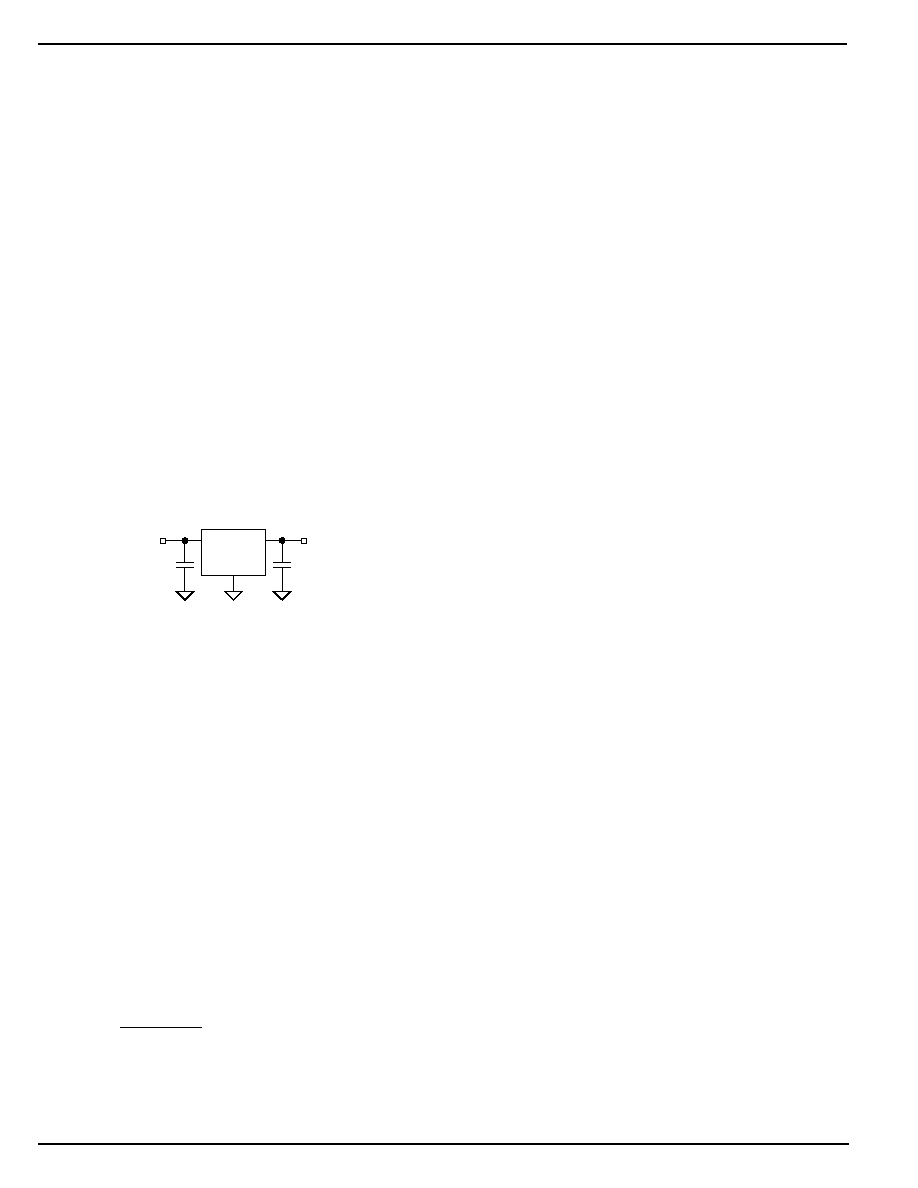
MIC39150-x.x
IN
OUT
GND
C
IN
C
OUT
V
IN
V
OUT
Figure 1. Capacitor Requirements
Thermal Design
Linear regulators are simple to use. The most complicated
design parameters to consider are thermal characteristics.
Thermal design requires the following application-specific
parameters:
∑ Maximum ambient temperature (T
A
)
∑ Output Current (I
OUT
)
∑ Output Voltage (V
OUT
)
∑ Input Voltage (V
IN
)
∑ Ground Current (I
GND
)
First, calculate the power dissipation of the regulator from
these numbers and the device parameters from this datasheet.
P
D
= (V
IN
≠ V
OUT
)
I
OUT
+ V
IN
I
GND
where the ground current is approximated by using numbers
from the "Electrical Characteristics" or "Typical Characteris-
tics." Then the heat sink thermal resistance is determined
with this formula:
SA
J(max)
A
D
JC
CS
T
T
P
=
-
-
+
(
)
Where T
J (max)
125
∞
C and
CS
is between 0
∞
and 2
∞
C/W.
The heat sink June be significantly reduced in applications
where the minimum input voltage is known and is large
compared with the dropout voltage. Use a series input
resistor to drop excessive voltage and distribute the heat
between this resistor and the regulator. The low dropout
properties of Micrel Super
eta PNP regulators allow signifi-
cant reductions in regulator power dissipation and the asso-
ciated heat sink without compromising performance. When
this technique is employed, a capacitor of at least 1
µ
F is
needed directly between the input and regulator ground.
Refer to
Application Note 9 for further details and examples
on thermal design and heat sink specification.
Output Capacitor
The MIC39150/1 requires an output capacitor to maintain
stability and improve transient response. Proper capacitor
selection is important to ensure proper operation. The
MIC39150/1 output capacitor selection is dependent upon
the ESR (equivalent series resistance) of the output capacitor
to maintain stability. When the output capacitor is 10
µ
F or
greater, the output capacitor should have an ESR less than
2
. This will improve transient response as well as promote
stability. Ultralow ESR capacitors (<100m
), such as ce-
ramic chip capacitors June promote instability. These very
low ESR levels June cause an oscillation and/or underdamped
transient response. A low-ESR solid tantalum capacitor works
extremely well and provides good transient response and
stability over temperature. Aluminum electrolytics can also
be used, as long as the ESR of the capacitor is < 2
.
The value of the output capacitor can be increased without
limit. Higher capacitance values help to improve transient
response and ripple rejection and reduce output noise.
Input Capacitor
An input capacitor of 1
µ
F or greater is recommended when
the device is more than 4 inches away from the bulk ac supply
capacitance, or when the supply is a battery. Small, surface-
mount, ceramic chip capacitors can be used for the bypass-
ing. The capacitor should be placed within 1" of the device for
optimal performance. Larger values will help to improve
ripple rejection by bypassing the input to the regulator, further
improving the integrity of the output voltage.
Transient Response and 3.3V to 2.5V
or 2.5V to 1.8V Conversion
The MIC39150/1 has excellent transient response to varia-
tions in input voltage and load current. The device has been
designed to respond quickly to load current variations and
input voltage variations. Large output capacitors are not
required to obtain this performance. A standard 10
µ
F output
capacitor, preferably tantalum, is all that is required. Larger
values help to improve performance even further.
By virtue of its low-dropout voltage, this device does not
saturate into dropout as readily as similar NPN-based de-
signs. When converting from 3.3V to 2.5V, or 2.5V to 1.8V, the
NPN-based regulators are already operating in dropout, with
typical dropout requirements of 1.2V or greater. To convert
down to 2.5V without operating in dropout, NPN-based
regulators require an input voltage of 3.7V at the very least.
The MIC39150/1 regulator will provide excellent performance
with an input as low as 3.0V or 2.5V, respectively. This gives

June 2001
9
MIC39150/39151
MIC39150/39151
Micrel
the PNP-based regulators a distinct advantage over older,
NPN-based linear regulators.
Minimum Load Current
The MIC39150 regulator is specified between finite loads. If
the output current is too small, leakage currents dominate
and the output voltage rises. A 10mA minimum load current
is necessary for proper regulation.
Error Flag
The MIC39151 version features an error flag circuit which
monitors the output voltage and signals an error condition
when the voltage 5% below the nominal output voltage. The
error flag is an open-collector output that can sink 10mA
during a fault condition.
Low output voltage can be caused by a number of problems,
including an overcurrent fault (device in current limit) or low
input voltage. The flag is inoperative during overtemperature
shutdown.
When the error flag is not used, it is best to leave it open. The
flag pin can be tied directly to pin 4, the output pin.
Enable Input
The MIC39151 version features an enable input for on/off
control of the device. Its shutdown state draws "zero" current
(only microamperes of leakage). The enable input is TTL/
CMOS compatible for simple logic interface, but can be
connected to up to 20V. When enabled, it draws approxi-
mately 15
µ
A.
MIC39150/39151
Micrel
MIC39150/39151
10
June 2001
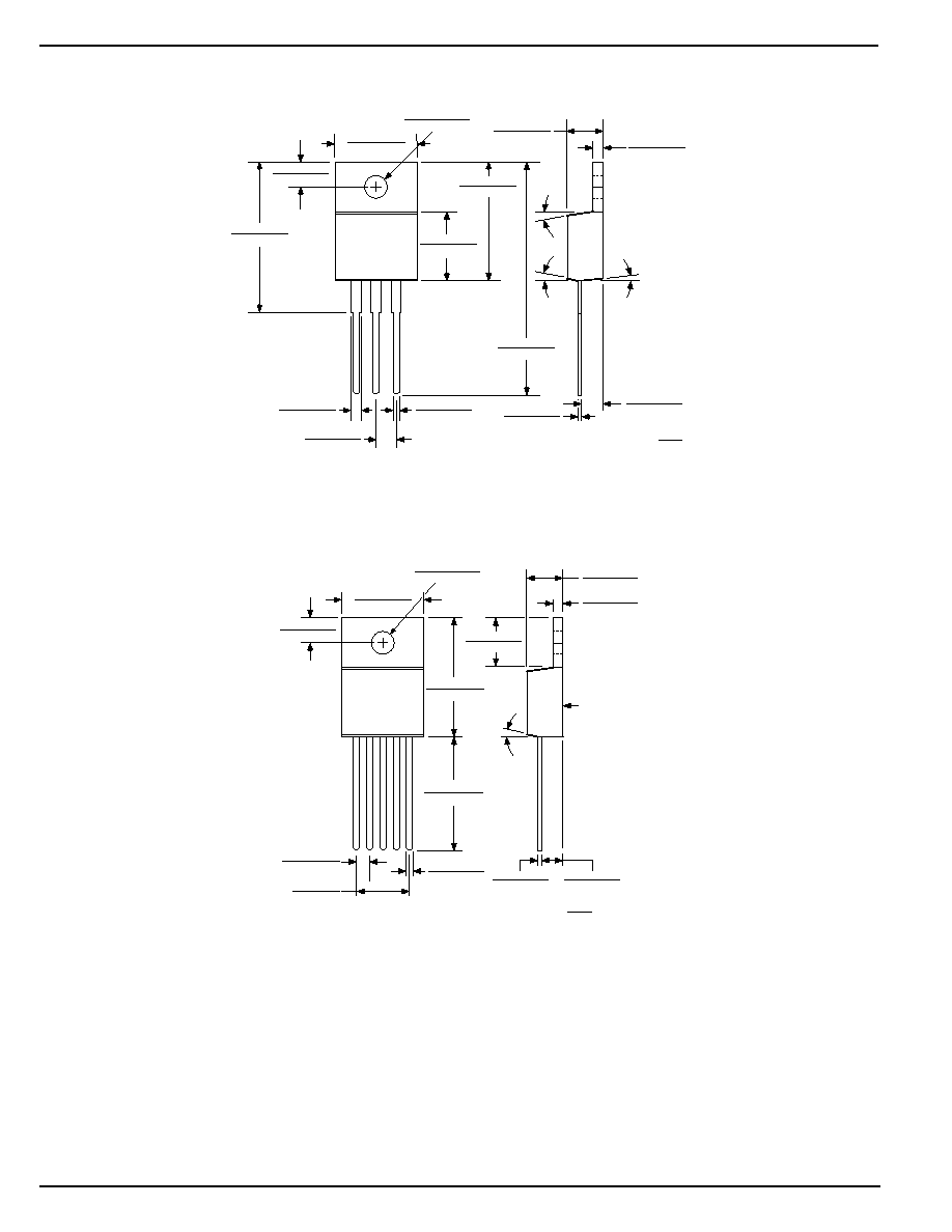
Package Information
0.018
±
0.008
(0.46
±
0.020)
0.100
±
0.005
(2.54
±
0.13)
0.030
±
0.003
(0.76
±
0.08)
0.050
±
0.003
(1.27
±
.08)
7
∞
1.140
±
0.010
(28.96
±
0.25)
0.356
±
0.005
(9.04
±
0.13)
0.590
±
0.005
(14.99
±
0.13)
0.108
±
0.005
(2.74
±
0.13)
0.050
±
0.005
(1.27
±
0.13)
0.151 D
±
0.005
(3.84 D
±
0.13)
0.410
±
0.010
(10.41
±
0.25)
0.176
±
0.005
(4.47
±
0.13)
0.100
±
0.020
(2.54
±
0.51)
0.818
±
0.005
(20.78
±
0.13)
7
∞
3
∞
DIMENSIONS: INCH
(MM)
3-Lead TO-220 (T)
0.018
±
0.008
(0.46
±
0.20)
0.268 REF
(6.81 REF)
0.032
±
0.005
(0.81
±
0.13)
0.550
±
0.010
(13.97
±
0.25)
7
∞
Typ.
SEATING
PLANE
0.578
±
0.018
(14.68
±
0.46)
0.108
±
0.005
(2.74
±
0.13)
0.050
±
0.005
(1.27
±
0.13)
0.150 D
±
0.005
(3.81 D
±
0.13)
0.400
±
0.015
(10.16
±
0.38)
0.177
±
0.008
(4.50
±
0.20)
0.103
±
0.013
(2.62
±
0.33)
0.241
±
0.017
(6.12
±
0.43)
0.067
±
0.005
(1.70
±
0.127)
inch
(mm)
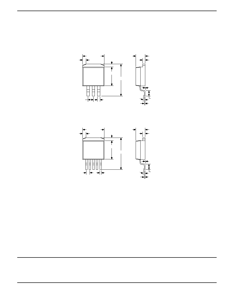
Dimensions:
5-Lead TO-220-5 (T)
June 2001
11
MIC39150/39151
MIC39150/39151
Micrel
0.360
±
0.005
0.600
±
0.025
0.405
±
0.005
0.100 BSC
0.050
0.050
±
0.005
0.176
±
0.005
8
∞
MAX
0.100
±
0.01
0.050
±
0.005
0.015
±
0.002
0.004+0.004
≠0.008
SEATING PLANE
0.065
±
0.010
20
∞±
2
∞
DIM. = INCH
3-Lead TO-263 (U)
0.067
±
0.005
0.032
±
0.003
0.360
±
0.005
0.600
±
0.025
0.405
±
0.005
0.060
±
0.005
0.176
±
0.005
8
∞
MAX
0.100
±
0.01
0.050
±
0.005
0.015
±
0.002
0.004+0.004
≠0.008
SEATING PLANE
0.065
±
0.010
20
∞±
2
∞
DIM. = INCH
5-Lead TO-263-5 (U)
MICREL INC.
1849 FORTUNE DRIVE
SAN JOSE, CA 95131
USA
TEL
+ 1 (408) 944-0800
FAX
+ 1 (408) 944-0970
WEB
http://www.micrel.com
This information is believed to be accurate and reliable, however no responsibility is assumed by Micrel for its use nor for any infringement of patents or
other rights of third parties resulting from its use. No license is granted by implication or otherwise under any patent or patent right of Micrel Inc.
© 2001 Micrel Incorporated