Äîêóìåíòàöèÿ è îïèñàíèÿ www.docs.chipfind.ru
MIC5156/5157/5158
Micrel
3-112
March 1999
MIC5156/5157/5158
Super LDOTM Regulator Controller
either 3.3V, 5.0V, or 12V. The MIC5158 can be configured as
a fixed 5V controller or programmed to any voltage from 1.3V
to 36V using two external resistors.
The MIC5156 is available in an 8-pin DIP or SOP. The
MIC5157 and MIC5158 are available in a 14-pin DIP or SOP
which operate from 40
°
C to +85
°
C.
Features
· 4.5mA typical operating current
· <1
µ
A typical standby current
· Low external parts count
· Optional current limit (35mV typical threshold)
· 1% initial output voltage tolerance in most configurations
· 2% output voltage tolerance over temperature
· Fixed output voltages of 3.3V, 5.0V (MIC5156)
· Fixed output voltages of 3.3V, 5.0V, 12V (MIC5157)
· Programmable (1.3 to 36V) with 2 resistors (MIC5156/8)
· Internal charge pump voltage tripler (MIC5157/8)
· Enable pin to activate or shutdown the regulator
· Internal gate-to-source protective clamp
· All versions available in DIP and SOP
Applications
· Ultrahigh current ultralow dropout voltage regulator
· Constant high-current source
· Low parts count 5.0V to 3.3V computer supply
· Low noise/low-dropout SMPS post regulator
· High-current, current-limited switch
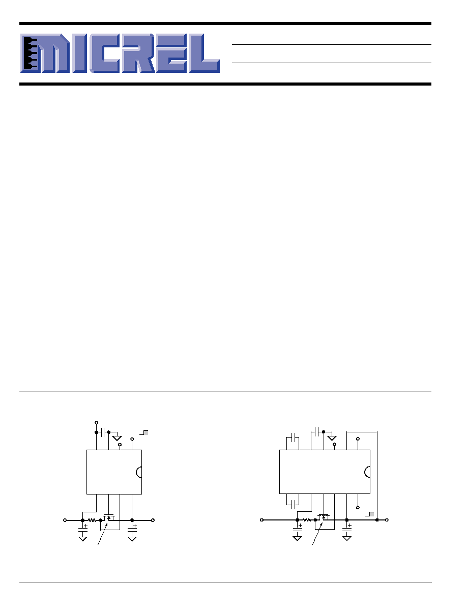
10A 5V to 3.3V Desktop Computer Regulator
General Description
The MIC5156, MIC5157, and MIC5158 Super Low-Dropout
(LDO) Regulator Controllers are single IC solutions for high-
current low-dropout linear voltage regulation. Super LDOTM
Regulators have the advantages of an external N-channel
power MOSFET as the linear pass element.
The MIC5156/7/8 family features a dropout voltage as low as
the R
DS(ON)
of the external power MOSFET multiplied by the
output current. The output current can be as high as the
largest MOSFETs can provide.
The MIC5156/7/8 family operates from 3V to 36V. The
MIC5156 requires an external gate drive supply to provide the
higher voltage needed to drive the gate of the external
MOSFET. The MIC5157 and MIC5158 each have an internal
charge pump tripler to produce the gate drive voltage. The
tripler is capable of providing enough voltage to drive a logic-
level MOSFET to 3.3V output from a 3.5V supply and is
clamped to 17.5V above the supply voltage. The tripler
requires three external capacitors.
The regulator output is constant-current limited when the
controller detects 35mV across an optional external sense
resistor. An active-low open-collector flag indicates a low
voltage of 8% or more below nominal output. A shutdown
(low) signal to the TTL-compatible enable control reduces
controller supply current to less than 1
µ
A while forcing the
output voltage to ground.
The MIC5156-3.3 and MIC5156-5.0 controllers have inter-
nally fixed output voltages. The MIC5156 [adjustable] output
is configured using two external resistors. The MIC5157 is a
fixed output controller which is externally configured to select
1
2
3
4
14
13
12
11
5
6
7
10
9
8
MIC5157
C2+
C2
V
CP
GND
FLAG
3.3V
5V
C1+
C1
V
DD
G
D
S
EN
V
OUT
3.3V, 10A
V
IN
(3.61V min.)
0.1µF
1.0µF
0.1µF
R
S
R
S
= 0.035V / I
LIMIT
3m
IRLZ44 (Logic Level MOSFET)
C
L
*
47µF
* Improves transient
response to load changes
Enable
Shutdown
47µF
10A Low-Dropout Voltage Regulator
1
2
3
8
7
6
4
5
MIC5156-3.3
V
P
GND
FLAG
EN
V
DD
G
D
S
V
OUT
3.3V, 10A
V
IN
5V
0.1µF
R
S
R
S
= 0.035V / I
LIMIT
3m
SMP60N03-10L
C
L
*
47µF
* Improves transient
response to load changes
+12V
Enable
Shutdown
47µF
Typical Applications
Super LDO is a trademark of Micrel, Inc.
March 1999
3-113
MIC5156/5157/5158
Micrel
3
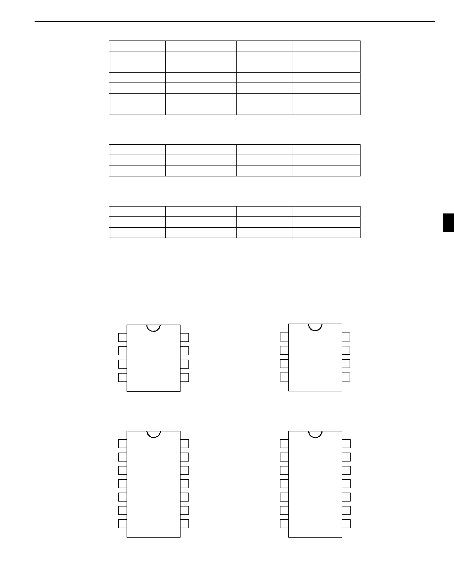
Pin Configuration
Ordering Information MIC5156
Part Number
Temperature Range
Voltage
Package
MIC5156-3.3BN
40
°
C to +85
°
C
3.3V
8-pin DIP
MIC5156-5.0BN
40
°
C to +85
°
C
5.0V
8-pin DIP
MIC5156BN
40
°
C to +85
°
C
Adjustable
8-pin DIP
MIC5156-3.3BM
40
°
C to +85
°
C
3.3V
8-pin SOP
MIC5156-5.0BM
40
°
C to +85
°
C
5.0V
8-pin SOP
MIC5156BM
40
°
C to +85
°
C
Adjustable
8-pin SOP
Ordering Information MIC5157
Part Number
Temperature Range
Voltage
Package
MIC5157BN
40
°
C to +85
°
C
Selectable
14-pin DIP
MIC5157BM
40
°
C to +85
°
C
Selectable
14-pin SOP
Ordering Information MIC5158
Part Number
Temperature Range
Voltage
Package
MIC5158BN
40
°
C to +85
°
C
5.0V/Adj.
14-pin DIP
MIC5158BM
40
°
C to +85
°
C
5.0V/Adj.
14-pin SOP
1
2
3
4
EN
FLAG
S (Source)
GND
V
P
D (Drain)
V
D D
G (Gate)
8
7
6
5
MIC5156-x.x
1
2
3
4
EA
5V FB
EN
FLAG
GND
S (Source)
G (Gate)
D (Drain)
14
13
12
11
MIC5158
5
6
7
V
CP
C2
C2+
V
D D
C1+
C1
10
9
8
1
2
3
4
5V
3.3V
EN
FLAG
GND
S (Source)
G (Gate)
D (Drain)
14
13
12
11
MIC5157
5
6
7
V
CP
C2
C2+
V
D D
C1+
C1
10
9
8
1
2
3
4
EN
FLAG
GND
V
P
D (Drain)
V
D D
G (Gate)
8
7
6
5
MIC5156
EA
MIC5156/5157/5158
Micrel
3-114
March 1999
Pin Description MIC5156
Pin Number
Pin Name
Pin Function
1
EN
Enable (Input): TTL high enables regulator; TTL low shuts down regulator.
2
FLAG
Output Flag (Output): Open collector output is active (low) when V
OUT
is more
than 8% below nominal output. Circuit has 3% hysteresis.
3
GND
Circuit ground.
4
V
P
N-channel Gate Drive Supply Voltage: User supplied voltage for driving the
gate of the external MOSFET.
5
V
DD
Supply Voltage (Input): Supply voltage connection. Connect sense resistor
(R
S
) to V
DD
if current limiting used. Connect supply bypass capacitor to
ground near device.
6
G
Gate (Output): Drives the gate of the external MOSFET.
7
D
Drain and Current Limit (Input): Connect to external MOSFET drain and
external sense resistor (current limit), or connect to V
DD
and external MOSFET
drain (no current limit).
8 (3.3V, 5V)
S
Source (Input): Top of internal resistive divider chain. Connect directly to the
load for best load regulation.
8 (adjustable)
EA
Error Amplifier (Input): Connect to external resistive divider.
Pin Description MIC5157, MIC5158
Pin Number
Pin Name
Pin Function
1 (MIC5157)
5V
5V Configuration (Input): Connect to S (source) pin for 5V output.
1 (MIC5158)
EA
Error Amplifier (Input): Connect to external resistive divider to obtain adjust-
able output.
2 (MIC5157)
3.3V
3.3V Configuration (Input): Connect to S (source) pin for 3.3V output.
2 (MIC5158)
5V FB
5V Feedback (Input): Connect to EA for fixed 5V output.
3
FLAG
Output Voltage Flag (Output): Open collector is active (low) when V
OUT
is 8%
or more below its nominal value.
4
GND
Circuit ground.
5
V
CP
Voltage Tripler Output [Filter Capacitor]. Connect a 1 to 10
µ
F capacitor to ground.
6
C2
Charge Pump Capacitor 2: Second stage of internal voltage tripler. Connect a
0.1
µ
F capacitor from C2+ to C2.
7
C2+
Charge Pump Capacitor 2: See C2 pin 6.
8
C1+
Charge Pump Capacitor 1: First stage of internal voltage tripler. Connect a
0.1
µ
F capacitor from C1+ to C1.
9
C1
Charge Pump Capacitor 1: See C1+ pin 8.
10
V
DD
Supply Voltage (Input): Supply voltage connection. Connect sense resistor
(R
S
) to V
DD
if current limiting used. Connect supply bypass capacitor to
ground near device.
11
G
Gate (Output): Connect to External MOSFET gate.
12
D
Drain and Current Limit (Input): Connect to external MOSFET drain and
external sense resistor (current limit), or connect to V
DD
and external MOSFET
drain (no current limit).
13 (MIC5157)
S
Source and 3.3V/5V Configuration: Top of internal resistor chain. Connect to
source of external MOSFET for 3.3V, 5V, and 12V operation. Also see 3.3V
and 5V pin descriptions.
13 (MIC5158)
S
Source (Input): Top of internal resistor chain. Connect to top of external
resistive divider and source of external MOSFET.
14
EN
Enable (Input): TTL high enables regulator; TTL low shuts down regulator.
March 1999
3-115
MIC5156/5157/5158
Micrel
3
Electrical Characteristics
V
DD
= 5V, V
EN
= 5V; T
A
= 25
°
C; unless noted.
Symbol
Parameter
Condition
Min
Typ
Max
Units
V
DD
Supply Voltage
3
36
V
I
DD(ON)
Supply Current MIC5156
Operating, V
EN
= 5V
2.7
10
mA
I
DD(OFF)
Shutdown, V
EN
= 0V
0.1
5
µ
A
I
DD(ON)
Supply Current MIC5157/8
Operating, V
EN
= 5V
4.5
10
mA
I
DD(OFF)
Shutdown, V
EN
= 0V
0.1
5
µ
A
V
IH
Enable Input Threshold
High
2.4
1.3
V
V
IL
Low
1.3
0.8
V
EN I
B
Enable Input Bias Current
V
EN
= 2.4V
20
25
µ
A
V
CP
Max. Charge Pump Voltage
V
CP
V
DD
, V
DD
> 10V
17.5
18.5
V
f
CP
Charge Pump Frequency
160
kHz
V
OUT MAX
Maximum Gate Drive Voltage
V
SOURCE
= 0V
(MIC5157/8)
V
DD
= 3.5V
5
7.0
9
V
V
DD
= 5V
9
11.3
15
V
V
DD
= 12V
24
28
30
V
V
OUT MIN
Minimum Gate Drive Voltage
V
SOURCE
> V
OUT(NOM)
1.0
V
V
LIM
Current Limit Threshold
V
DD
V
D
@ I
LIM
28
35
42
mV
V
S
Source Voltage
Short G (gate) to (S) source, Note 4
MIC5156-3.3
3.267
3.3
3.333
V
MIC5156-5.0
4.950
5.0
5.050
V
MIC5157, 3.3V pin to S pin (3.3V config.)
3.250
3.3
3.350
V
MIC5157, 5V pin to S pin (5V config.)
4.950
5.0
5.050
V
MIC5157, V
DD
= 7V, (12V config.)
11.70
12
12.30
V
MIC5158, 5V FB pin to EA pin (5V config.)
4.925
5.0
5.075
V
V
BG
Bandgap Reference Voltage
MIC5156 [adjustable] and MIC5158
1.222
1.235
1.248
V
V
LR
Output Voltage Line Regulation
5V < V
DD
< 15V, V
OUT
= 3.3V
2
7
mV
V
GS MAX
Gate to Source Clamp
14
16.6
20
V
V
FT
Flag Comparator Threshold
% of nominal V
SOURCE
92
%
V
FH
Flag Comparator Hysteresis
% of nominal V
SOURCE
3
%
V
SAT
Flag Comparator Sat. Voltage
I
FLAG
= 1mA
0.09
0.2
V
Note 1.
Exceeding the absolute maximum rating may damage the device.
Note 2.
The device is not guaranteed to function outside its operating rating.
Note 3.
Devices are ESD sensitive. Handling precautions recommended.
Note 4.
Test configuration. External MOSFET not used.
Absolute Maximum Ratings
(Note 1)
Supply Input (V
DD
) ...................................................... +38V
Enable Input (V
EN
) ......................................... 0.3V to 36V
Gate Output (V
G
) MIC5156 ......................................... +55V
Charge Pump Node (V
CP
) MIC5157/8 ........................ +55V
Source Connection (V
S
) .................................... 1.3 to +36V
Flag (V
FLAG
) .................................................... 0.3 to +40V
Storage Temperature (T
S
) ....................... 65
°
C to +150
°
C
Lead Temperature (soldering 10 sec.) ...................... 300
°
C
Operating Ratings
(Note 2)
Ambient Temperature Range (T
A
)
MIC515xBM/BN ..................................... 40
°
C to +85
°
C
Junction Temperature (T
J
) ...................................... +150
°
C
Thermal Resistance (
JA
)
Package
MIC5156
MIC5157/8
DIP ............................... 100
°
C/W ..................... 90
°
C/W
SOP .............................. 160
°
C/W ................... 120
°
C/W
MIC5156/5157/5158
Micrel
3-116
March 1999
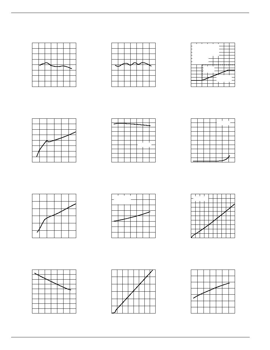
Typical Characteristics
3.26
3.27
3.28
3.29
3.30
3.31
3.32
3.33
3.34
-60 -30
0
30
60
90 120 150
OUTPUT VOLTAGE (V)
TEMPERATURE (
°
C)
3.3V Regulator Output
Voltage vs. Temperature
4.96
4.97
4.98
4.99
5.00
5.01
5.02
5.03
5.04
-60 -30
0
30
60
90 120 150
OUTPUT VOLTAGE (V)
TEMPERATURE (
°
C)
5.0V Regulator Output
Voltage vs. Temperature
2.0
3.0
4.0
5.0
6.0
7.0
8.0
9.0
10.0
0
5
10
15
20
25
30
ON-STATE SUPPLY CURRENT (mA)
SUPPLY VOLTAGE (V)
MIC5157/8 On-State Supply
Current vs. Supply Voltage
0.0
0.5
1.0
1.5
2.0
2.5
3.0
3.5
4.0
4.5
5.0
-60 -30
0
30
60
90 120 150
ON-STATE SUPPLY CURRENT (mA)
TEMPERATURE (
°
C)
MIC5157/8 On-State Supply
Current vs. Temperature
V
DD
= 5V
0.0
0.5
1.0
1.5
2.0
2.5
3.0
3.5
4.0
4.5
5.0
-60 -30
0
30
60
90 120 150
OFF-STATE SUPPLY CURRENT (
µ
A)
TEMPERATURE (
°
C)
Off-State Supply Current
vs. Temperature
V
DD
= 5V
0
10
20
30
40
50
60
0
5
10
15
20
25
30
CHARGE PUMP VOLTAGE (V)
SUPPLY VOLTAGE (V)
Charge-Pump Output Voltage
vs. Supply Voltage
0
25
50
75
100
125
150
175
200
-60 -30
0
30
60
90 120 150
FLAG VOLTAGE (mV)
TEMPERATURE (
°
C)
Flag Output Voltage
vs. Temperature
V
DD
= 5V
I
FLAG
= 1mA
0.0
0.2
0.4
0.6
0.8
1.0
1.2
1.4
1.6
1.8
-60 -30
0
30
60
90 120 150
ENABLE THRESHOLD VOLTAGE (V)
TEMPERATURE (
°
C)
Enable Threshold Voltage
vs. Temperature
0
10
20
30
40
50
60
70
-60 -30
0
30
60
90 120 150
CURRENT LIMIT THRESHOLD (mV)
TEMPERATURE (
°
C)
Current Limit Threshold
vs. Temperature
-2
0
2
4
6
8
10
12
-0.2
0.0
0.2
0.4
0.6
VOLTAGE (V)
TIME (ms)
MIC5157/8 Turn-On
Response Time for 3.3V
C
CP
= 1
µ
F
C
L
= 50
µ
F
LOGIC
INPUT
3.3V
OUTPUT
MOSFET = IRF540
V
IN
= 5V, I
L
= 0.5A
C
C1
= C
C2
= 0.1
µ
F
0.0
0.1
0.2
0.3
0.4
0.5
0.6
0.7
0.8
0.9
1.0
0
2
4
6
8
10
FLAG VOLTAGE (V)
FLAG SINK CURRENT (mA)
Flag Output Voltage
vs. Flag Current
V
DD
= 5V
0
20
40
60
80
100
120
0
2
4
6
8
10 12 14 16
ENABLE BIAS CURRENT (
µ
A)
ENABLE VOLTAGE (V)
Enable Input Bias Current
vs. Enable Voltage