/home/web/doc/html/micrel/181742
MIC5200
Micrel
MIC5200
1
July 1998
MIC5200-3.3
Enable
Output
MIC5200
100mA Low-Dropout Regulator
Final Information
General Description
The MIC5200 is an efficient linear voltage regulator with very
low dropout voltage (typically 17mV at light loads and 200mV
at 100mA), and very low ground current (1mA at 100mA
output), offering better than 1% initial accuracy with a logic
compatible ON/OFF switching input. Designed especially for
hand-held battery powered devices, the MIC5200 is switched
by a CMOS or TTL compatible logic signal. The ENABLE
control may be tied directly to V
IN
if unneeded. When disabled,
power consumption drops nearly to zero. The ground current
of the MIC5200 increases only slightly in dropout, further
prolonging battery life. Key MIC5200 features include protec-
tion against reversed battery, current limiting, and over-
temperature shutdown.
The MIC5200 is available in several fixed voltages and
accuracy configurations. Other options are available; contact
Micrel for details.
Features
· High output voltage accuracy
· Variety of output voltages
· Guaranteed 100mA output
· Low quiescent current
· Low dropout voltage
· Extremely tight load and line regulation
· Very low temperature coefficient
· Current and thermal limiting
· Zero OFF mode current
· Logic-controlled electronic shutdown
· Available in 8-lead SOIC, MM8TM 8-lead MSOP,
and SOT-223 packages
Applications
· Cellular Telephones
· Laptop, Notebook, and Palmtop Computers
· Battery Powered Equipment
· PCMCIA V
CC
and V
PP
Regulation/Switching
· Bar Code Scanners
· SMPS Post-Regulator/ DC to DC Modules
· High Efficiency Linear Power Supplies
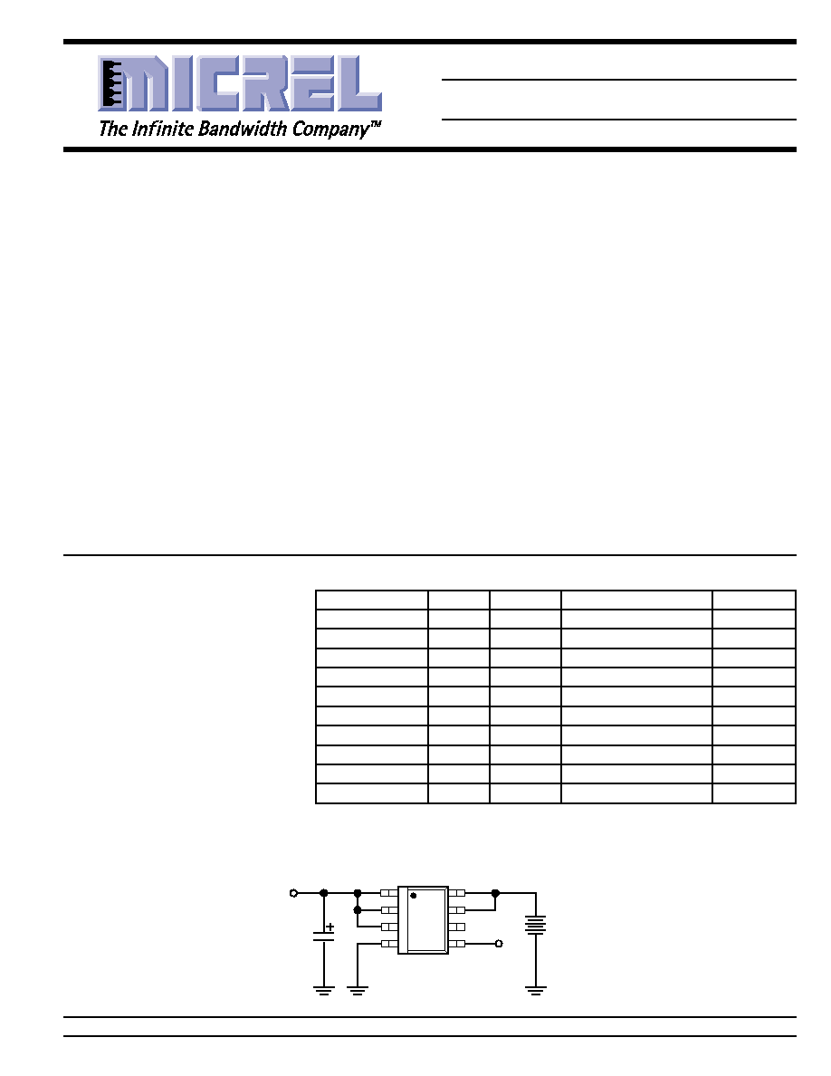
Typical Application
1
µ
F
Ordering Information
Part Number
Voltage
Accuracy
Junction Temp. Range*
Package
MIC5200-3.0BM
3.0
1%
40
°
C to +125
°
C
8-Pin SOP
MIC5200-3.3BM
3.3
1%
40
°
C to +125
°
C
8-Pin SOP
MIC5200-4.8BM
4.85
1%
40
°
C to +125
°
C
8-Pin SOP
MIC5200-5.0BM
5.0
1%
40
°
C to +125
°
C
8-Pin SOP
MIC5200-3.3BMM
3.3V
1%
40
°
C to +125
°
C
8-Pin MSOP
MIC5200-5.0BMM
5.0V
1%
40
°
C to +125
°
C
8-Pin MSOP
MIC5200-3.0BS
3.0
1%
40
°
C to +125
°
C
SOT-223
MIC5200-3.3BS
3.3
1%
40
°
C to +125
°
C
SOT-223
MIC5200-4.8BS
4.85
1%
40
°
C to +125
°
C
SOT-223
MIC5200-5.0BS
5.0
1%
40
°
C to +125
°
C
SOT-223
Other voltages available. Contact Micrel for details.
Micrel, Inc. · 1849 Fortune Drive · San Jose, CA 95131 · USA · tel + 1 (408) 944-0800 · fax + 1 (408) 944-0970 · http://www.micrel.com
MIC5200
Micrel
July 1998
2
MIC5200
Absolute Maximum Ratings
Power Dissipation ............................................... Internally Limited
Lead Temperature (soldering, 5 sec.) .................................. 260
°
C
Operating Junction Temperature Range ............. 40
°
C to +125
°
C
Input Supply Voltage ................................................ 20V to +60V
Enable Input Voltage ................................................ 20V to +60V
Thermal Characteristics
SOT-223
(
JC
) ..................................................................... 15
°
C/W
SO-8
(
JA
) ..................................................................... See Note 1
Absolute Maximum Ratings indicate limits beyond which damage
to the device may occur. Electrical specifications do not apply when
operating the device beyond its specified Operating Ratings.
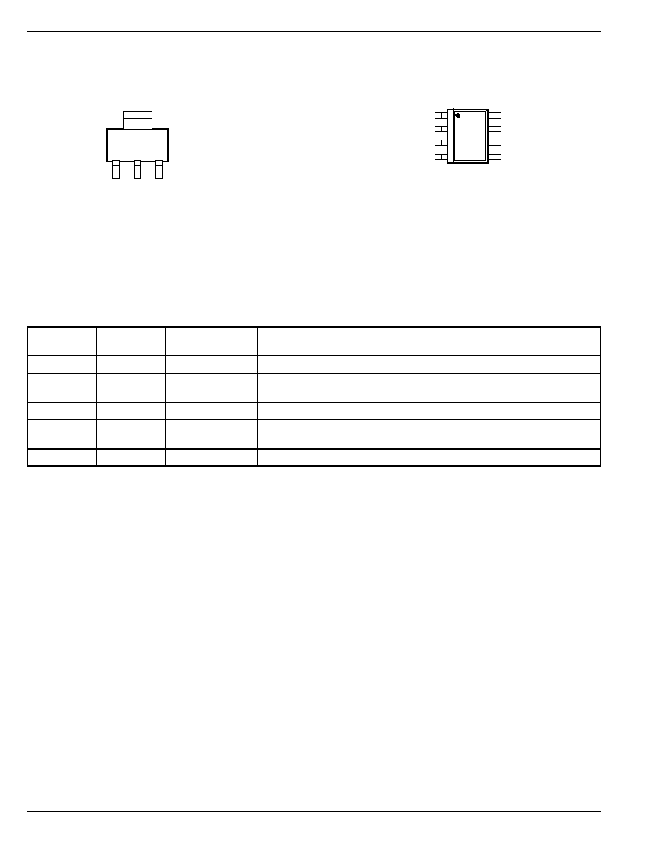
Pin Description
Pin Number
Pin Number
Pin Name
Pin Function
SOT-223
SO-8, MSOP-8
3
1, 2
OUT
Output: Pins 1 and 2 must be externally connected together.
3, 6
NC
(not internally connected): Connect to ground plane for lowest thermal
resistance.
2,
TAB
4
GND
Ground: Ground pin and
TAB
are internally connected.
5
EN
Enable/Shutdown (Input): TTL compatible input. High = enabled;
low = shutdown.
1
7, 8
IN
Supply Input: Pins 7 and 8 must be extenally connected together.
EN may be tied directly to V
IN
Pin Configuration
1
2
3
IN GND OUT
MIC5200-x.xBS
(SOT-223)
Recommended Operating Conditions
Input Voltage ............................................................... 2.5V to 26V
Operating Junction Temperature Range ............. 40
°
C to +125
°
C
Enable Input Voltage .................................................... 20V to V
IN
GND
OUT
IN
EN
MIC5200-x.xBM
(SO-8)
MIC5200-x.xBMM
(MSOP-8)
OUT
NC
IN
NC
MIC5200
Micrel
MIC5200
3
July 1998
Electrical Characteristics
Limits in standard typeface are for T
J
= 25
°
C and limits in boldface apply over the junction temperature range of 40
°
C to +125
°
C.
Unless otherwise specified, V
IN
= V
OUT
+ 1V, I
L
= 1mA, C
L
= 3.3
µ
F, and V
ENABLE
2.0V
Symbol
Parameter
Conditions
Min
Typical
Max
Units
V
O
Output Voltage
Variation from specified V
OUT
1
1
%
Accuracy
2
2
V
O
Output Voltage
(Note 2)
40
150
ppm/
°
C
T
Temperature Coef.
V
O
Line Regulation
V
IN
= V
OUT
+ 1 V to 26V
0.004
0.10
%
V
IN
0.40
V
O
Load Regulation
I
L
= 0.1mA to 100mA (Note 3)
0.04
0.16
%
V
OUT
0.30
V
IN
V
O
Dropout Voltage
I
L
= 100
µ
A
17
mV
(Note 4)
I
L
= 20mA
130
I
L
= 30mA
150
I
L
= 50mA
190
I
L
= 100mA
230
350
I
GND
Quiescent Current
V
ENABLE
0.7V (Shutdown)
0.01
10
µ
A
I
GND
Ground Pin Current
V
ENABLE
2.0V, I
L
= 100
µ
A
130
µ
A
I
L
= 20mA
270
350
I
L
= 30mA
330
I
L
= 50mA
500
I
L
= 100mA
1000
1500
PSRR
Ripple Rejection
70
dB
I
GNDDO
Ground Pin
V
IN
= 0.5V less than specified V
OUT
270
330
µ
A
Current at Dropout
I
L
= 100
µ
A (Note 5)
I
LIMIT
Current Limit
V
OUT
= 0V
100
250
mA
V
O
Thermal Regulation
(Note 6)
0.05
%/W
P
D
e
n
Output Noise
100
µ
V
ENABLE Input
Input Voltage Level
V
IL
Logic Low
OFF
0.7
V
Logic High
ON
2.0
I
IL
ENABLE Input Current
V
IL
0.7V
0.01
1
µ
A
I
IH
V
IH
2.0V
15
50
Note 1:
Absolute maximum ratings indicate limits beyond which damage to the component may occur. Electrical specifications do not
apply when operating the device outside of its rated operating conditions. The maximum allowable power dissipation is a
function of the maximum junction temperature, T
J (MAX)
, the junction-to-ambient thermal resistance,
JA
, and the ambient
temperature, T
A
. The maximum allowable power dissipation at any ambient temperature is calculated using: P
(MAX)
=
(T
J(MAX)
T
A
)
÷
JA
. Exceeding the maximum allowable power dissipation will result in excessive die temperature, and the
regulator will go into thermal shutdown. The
JC
of the MIC5200-xxBS is 15
°
C/W and
JA
for the MIC5200BM is 160
°
C/W
mounted on a PC board (see "Thermal Considerations" section for further details).
Note 2:
Output voltage temperature coefficient is defined as the worst case voltage change divided by the total temperature range.
Note 3:
Regulation is measured at constant junction temperature using low duty cycle pulse testing. Parts are tested for load regulation
in the load range from 0.1mA to 100mA. Changes in output voltage due to heating effects are covered by the thermal regulation
specification.
Note 4:
Dropout Voltage is defined as the input to output differential at which the output voltage drops 2% below its nominal value
measured at 1V differential.
Note 5:
Ground pin current is the regulator quiescent current plus pass transistor base current. The total current drawn from the supply
is the sum of the load current plus the ground pin current.
Note 6:
Thermal regulation is defined as the change in output voltage at a time t after a change in power dissipation is applied, excluding
load or line regulation effects. Specifications are for a 100mA load pulse at V
IN
= 26V for t = 10ms.
MIC5200
Micrel
July 1998
4
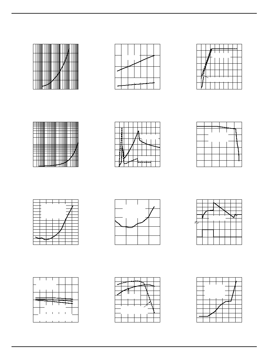
MIC5200
0.15
0.20
0.25
0.30
-60 -30
0
30
60
90 120 150
GROUND CURRENT (mA)
TEMPERATURE (
°
C)
Ground Current
vs. Temperature
I
LOAD
= 100
µ
A
C
IN
= 2.2
µ
F
C
OUT
= 4.7
µ
F
1.0
1.1
1.2
1.3
1.4
1.5
-50
0
50
100
150
GROUND CURRENT (mA)
TEMPERATURE (
°
C)
Ground Current
vs. Temperature
I
LOAD
= 100mA
C
IN
= 2.2
µ
F
C
OUT
= 4.7
µ
F
-100
0
100
200
-5
0
5
10 15 20 25 30 35
LOAD (mA)
TIME (ms)
Thermal Regulation
(3.3V Version)
-50
0
50
100
OUTPUT (mV)
C
L
= 4.7
µ
F
3.0
3.1
3.2
3.3
3.4
3.5
3.6
-60 -30
0
30
60
90 120 150
OUTPUT VOLTAGE (V)
TEMPERATURE (
°
C)
Output Voltage vs. Temp.
(3.3V Version)
C
IN
= 2.2
µ
F
C
OUT
= 4.7
µ
F
3 DEVICES:
HI / AVG / LO
CURVES APPLICABLE
AT 100
µ
A AND 100mA
100
120
140
160
180
200
220
240
260
280
300
-60 -30
0
30
60
90 120 150
OUTPUT CURRENT (mA)
TEMPERATURE (
°
C)
Output Current
vs. Temperature
V
OUT
= 0V
(SHORT CIRCUIT)
V
OUT
= 3.3V
3.20
3.21
3.22
3.23
3.24
3.25
3.26
3.27
3.28
3.29
3.30
-60 -30
0
30
60
90 120 150
MIN. INPUT VOLTAGE (V)
TEMPERATURE (
°
C)
Minimum Input Voltage
vs. Temperature
C
IN
= 2.2
µ
F
C
OUT
= 4.7
µ
F
I
LOAD
= 1mA
0
50
100
150
200
250
0.01
0.1
1
10
100
1000
DROPOUT VOLTAGE (mV)
OUTPUT CURRENT (mA)
Dropout Voltage
vs. Output Current
0.0
0.1
0.2
0.3
0.4
-60 -30
0
30
60
90 120 150
DROPOUT VOLTAGE (V)
TEMPERATURE (
°
C)
Dropout Voltage
vs. Temperature
I
L
= 100mA
I
L
= 1mA
0.0
0.5
1.0
1.5
2.0
2.5
3.0
3.5
0
2
4
6
8
10
OUTPUT VOLTAGE (V)
INPUT VOLTAGE (V)
Dropout
Characteristics
I
L
= 100mA
I
L
= 100
µ
A, 1mA
0.1
1
10
0.01
0.1
1
10
100
GROUND CURRENT (mA)
OUTPUT CURRENT (mA)
Ground Current
vs. Output Current
0.0
0.2
0.4
0.6
0.8
1.0
1.2
1.4
1.6
0
2
4
6
8
10
GROUND CURRENT (mA)
SUPPLY VOLTAGE (V)
Ground Current
vs. Supply Voltage
I
L
= 100mA
I
L
= 1mA
0.0
0.5
1.0
1.5
2.0
2.5
3.0
3.5
0.0
0.1
0.2
0.3
OUTPUT VOLTAGE (V)
OUTPUT CURRENT (A)
Output Voltage
vs. Output Current
C
IN
= 2.2
µ
F
C
OUT
= 4.7
µ
F
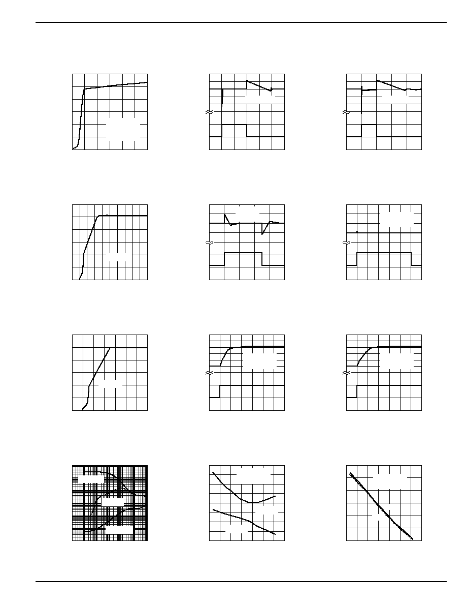
Typical Characteristics
MIC5200
Micrel
MIC5200
5
July 1998
0
50
100
150
200
250
300
1
2
3
4
5
6
7
SHORT CIRCUIT CURRENT (mA)
INPUT VOLTAGE (V)
Short Circuit Current
vs. Input Voltage
C
IN
= 2.2
µ
F
C
OUT
= 4.7
µ
F
V
OUT
= 3.3V
-30
-20
-10
0
10
20
OUTPUT (mV)
0
100
200
300
-2
0
2
4
6
8
10
OUTPUT (mA)
TIME (ms)
Load Transient
C
L
= 4.7
µ
F
0
100
200
300
-10
0
10
20
30
40
OUTPUT (mA)
TIME (ms)
Load Transient
-30
-20
-10
0
10
20
OUTPUT (mV)
C
L
= 47
µ
F
0
20
40
60
80
100
120
0
1
2
3
4
5
6
7
8
9 10
SUPPLY CURRENT (mA)
SUPPLY VOLTAGE (V)
Supply Current vs. Supply
Voltage (3.3V Version)
R
L
= 33
-10
-5
0
5
10
OUTPUT (mV)
2
4
6
8
-0.2
0
0.2
0.4
0.6
0.8
INPUT (V)
TIME (ms)
Line Transient
C
L
= 1
µ
F
I
L
= 1mA
-5
0
5
10
15
OUTPUT (mV)
2
4
6
8
-0.1
0
0.1 0.2 0.3 0.4 0.5 0.6
INPUT (V)
TIME (ms)
Line Transient
C
L
= 10
µ
F
I
L
= 1mA
0
10
20
30
40
50
60
0
1
2
3
4
5
6
7
SUPPLY CURRENT (mA)
SUPPLY VOLTAGE (V)
Supply Current vs. Supply
Voltage (3.3V Version)
R
L
= 66
-1
0
1
2
3
4
5
OUTPUT (V)
-2
0
2
4
-50
0
50 100 150 200 250 300
ENABLE (V)
TIME (
µ
s)
Enable Transient
(3.3V Version)
C
L
= 4.7
µ
F
I
L
= 1mA
-1
0
1
2
3
4
5
OUTPUT (V)
-2
0
2
4
-50
0
50 100 150 200 250 300
ENABLE (V)
TIME (
µ
s)
Enable Transient
(3.3V Version)
C
L
= 4.7
µ
F
I
L
= 100mA
0.001
0.01
0.1
1
10
100
1000
1x10
0
10x10
0
100x10
0
1x10
3
10x10
3
100x10
3
1x10
6
OUTPUT IMPEDANCE (
)
FREQUENCY (Hz)
Output Impedance
I
L
= 100
µ
A
I
L
= 1mA
I
L
= 100mA
-5
0
5
10
15
20
25
30
35
-60 -30
0
30
60
90 120 150
ENABLE CURRENT (
µ
A)
TEMPERATURE (
°
C)
Enable Current Threshold
vs. Temperature
C
IN
= 2.2
µ
F
C
OUT
= 4.7
µ
F
V
EN
= 2V
V
EN
= 5V
0.4
0.6
0.8
1
1.2
1.4
1.6
-60 -30
0
30
60
90 120 150
ENABLE VOLTAGE (V)
TEMPERATURE (
°
C)
Enable Voltage Threshold
vs. Temperature
C
IN
= 2.2
µ
F
C
OUT
= 4.7
µ
F
OFF
ON