
August 2003
1
MIC5239
MIC5239
Micrel
MIC5239
Low Quiescent Current 500mA
µ
Cap LDO Regulator
General Description
The MIC5239 is a low quiescent current,
µ
Cap low-dropout
regulator. With a maximum operating input voltage of 30V
and a quiescent current of 23
µ
A, it is ideal for supplying keep-
alive power in systems with high voltage batteries.
Capable of 500mA output, the MIC5239 has a dropout
voltage of only 350mV. It can provide high output current for
applications such as USB.
As a
µ
Cap LDO, the MIC5239 is stable with either a ceramic
or a tantalum output capacitor. It only requires a 3.3
µ
F output
capacitor for stability.
The MIC5239 includes a logic compatible enable input and an
undervoltage error flag indicator. Other features of the
MIC5239 include thermal shutdown, current limit, overvolt-
age shutdown, reverse-leakage protection, and reverse-
battery protection.
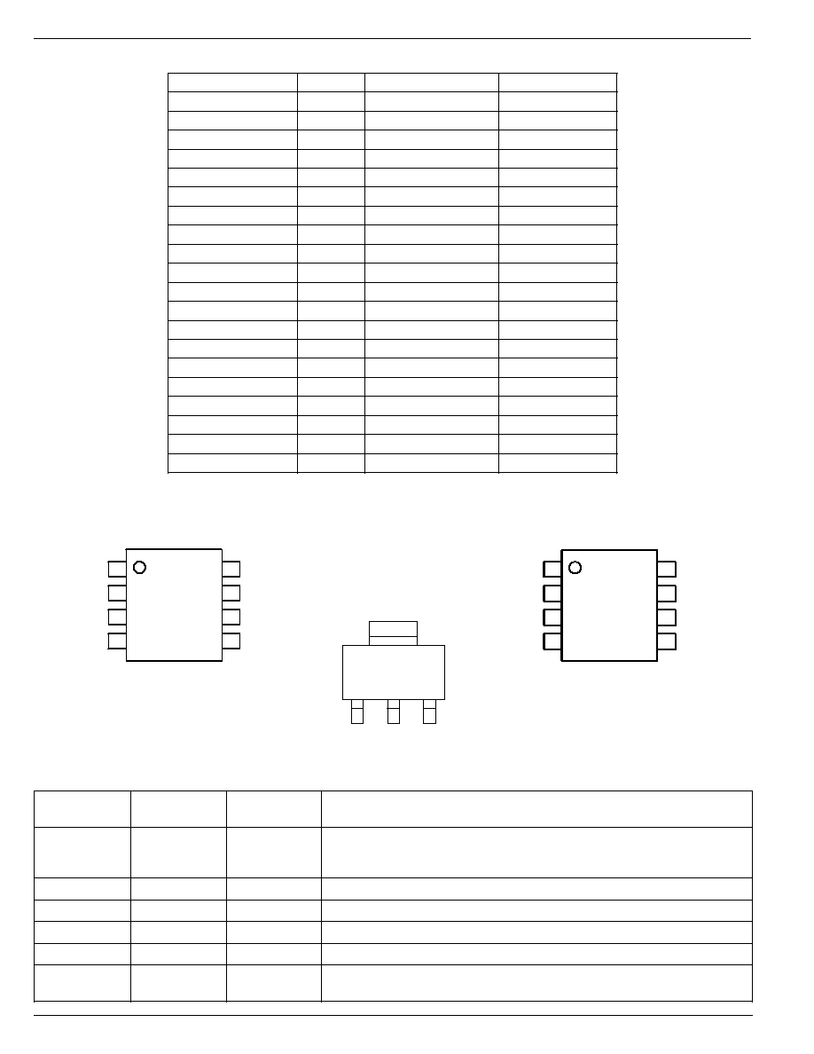
Available in the thermally enhanced SOIC-8, MSOP-8 and
SOT-223, the MIC5239 comes in fixed 1.5V, 1.8V, 2.5V,
3.0V, 3.3V and 5.0V, and adjustable voltages. For other
output voltages, contact Micrel.
Data sheets and support documentation can be found on
Micrel's web site at www.micrel.com.
Typical Application
I
GND
= 23
µ
A
V
OUT
3.0V/100
µ
A
V
IN
30V
IN
MIC5239
EN
OUT
GND
FLG
Regulator with Low I
O
and Low I
Q
Features
∑ Ultra-low quiescent current (I
Q
= 23
µ
A @I
O
= 100
µ
A)
∑ Continuous 500mA output current
∑ Wide input range: 2.3V to 30V
∑ Low dropout voltage:
350mV @500mA;
∑
±
1.0% initial output accuracy
∑ Stable with ceramic or tantalum output capacitor
∑ Logic compatible enable input
∑ Low output voltage error flag indicator
∑ Overcurrent protection
∑ Thermal shutdown
∑ Reverse-leakage protection
∑ Reverse-battery protection
∑ High-power SOIC-8, MSOP-8 and SOT-223 packages
Applications
∑ USB power supply
∑ Keep-alive supply in notebook and portable personal
computers
∑ Logic supply from high voltage batteries
∑ Automotive electronics
∑ Battery-powered systems
Micrel, Inc. ∑ 1849 Fortune Drive ∑ San Jose, CA 95131 ∑ USA ∑ tel + 1 (408) 944-0800 ∑ fax + 1 (408) 944-0970 ∑ http://www.micrel.com
Ground Current vs. Input Voltage
10
15
20
25
30
35
40
4
9
14
19
24
29
GROUND CURRENT (
µ
A)
INPUT VOLTAGE (V)
I
OUT
= 10
µ
A
I
OUT
= 1mA
I
OUT
= 100
µ
A
MIC5239
Micrel
MIC5239
2
August 2003
Pin Description
Pin Number
Pin Number
Pin Name
Pin Function
MSOP-8/SOIC-8
SOT-223
2 (Fixed)
-
FLG
Error FLAG (Output): Open-collector output is active low when the output is
out of regulation due to insufficient input voltage or excessive load. An
external pull-up resistor is required.
2 (Adj.)
-
ADJ
Adjustable Feedback Input: Connect to voltage divider network.
3
1
IN
Power Supply Input.
4
3
OUT
Regulated Output.
1
-
EN
Enable (Input): Logic low = shutdown; logic high = enabled.
5≠8
2
GND
Ground: Pins 5, 6, 7, and 8 are internally connected in common via the
leadframe.
Pin Configuration
EN
FLG
IN
OUT
GND
GND
GND
GND
1
2
3
4
8
7
6
5
SOIC-8 (M)
MSOP-8 (MM)
(Fixed)
Ordering Information
Part Number
Voltage
Junction Temp. Range
Package
MIC5239-1.5BMM
1.5V
≠40
∞
C to +125
∞
C
8-lead MSOP
MIC5239-1.5BM
1.5V
≠40
∞
C to +125
∞
C
8-lead SOIC
MIC5239-1.5BS
1.5V
≠40
∞
C to +125
∞
C
SOT-223
MIC5239-1.8BMM
1.8V
≠40
∞
C to +125
∞
C
8-lead MSOP
MIC5239-1.8BM
1.8V
≠40
∞
C to +125
∞
C
8-lead SOIC
MIC5239-1.8BS
1.8V
≠40
∞
C to +125
∞
C
SOT-223
MIC5239-2.5BMM
2.5V
≠40
∞
C to +125
∞
C
8-lead MSOP
MIC5239-2.5BM
2.5V
≠40
∞
C to +125
∞
C
8-lead SOIC
MIC5239-2.5BS
2.5V
≠40
∞
C to +125
∞
C
SOT-223
MIC5239-3.0BMM
3.0V
≠40
∞
C to +125
∞
C
8-lead MSOP
MIC5239-3.0BM
3.0V
≠40
∞
C to +125
∞
C
8-lead SOIC
MIC5239-3.0BS
3.0V
≠40
∞
C to +125
∞
C
SOT-223
MIC5239-3.3BMM
3.3V
≠40
∞
C to +125
∞
C
8-lead MSOP
MIC5239-3.3BM
3.3V
≠40
∞
C to +125
∞
C
8-lead SOIC
MIC5239-3.3BS
3.3V
≠40
∞
C to +125
∞
C
SOT-223
MIC5239-5.0BMM
5.0V
≠40
∞
C to +125
∞
C
8-lead MSOP
MIC5239-5.0BM
5.0V
≠40
∞
C to +125
∞
C
8-lead SOIC
MIC5239-5.0BS
5.0V
≠40
∞
C to +125
∞
C
SOT-223
MIC5239BMM
ADJ
≠40
∞
C to +125
∞
C
8-lead MSOP
MIC5239BM
ADJ
≠40
∞
C to +125
∞
C
8-lead SOIC
EN
ADJ
IN
OUT
GND
GND
GND
GND
1
2
3
4
8
7
6
5
SOIC-8 (M)
MSOP-8 (MM)
(Adj.)
IN
OUT
GND
1
3
2
TAB
GND
SOT-223 (S)
August 2003
3
MIC5239
MIC5239
Micrel
Absolute Maximum Ratings
(Note 1)
Supply Voltage (V
IN
) ..................................... ≠20V to +32V
Enable Input Voltage (V
EN
) .......................... ≠0.3V to +32V
Power Dissipation (P
D
), Note 3 ............... Internally Limited
Junction Temperature (T
J
) ....................... ≠40
∞
C to +125
∞
C
Storage Temperature (T
S
) ....................... ≠65
∞
C to +150
∞
C
Lead Temperature (soldering, 5 sec.) ....................... 260
∞
C
ESD Rating, Note 4
Operating Ratings
(Note 2)
Supply Voltage (V
IN
) ........................................ 2.3V to 30V
Enable Input Voltage (V
EN
) ................................. 0V to 30V
Junction Temperature (T
J
) ....................... ≠40
∞
C to +125
∞
C
Package Thermal Resistance
MSOP
(
JA
) ......................................................... 80
∞
C/W
SOT-223
(
JA
) ..................................................... 50
∞
C/W
Electrical Characteristics
(Note 5)
V
IN
= V
OUT
+ 1V; V
EN
2.0V; I
OUT
= 100
µ
A; T
J
= 25
∞
C, bold values indicate ≠40
∞
C
T
J
+125
∞
C; unless noted.
Symbol
Parameter
Conditions
Min
Typ
Max
Units
V
OUT
Output Voltage Accuracy
variation from nominal V
OUT
≠1
1
%
≠2
+2
%
V
OUT
/V
OUT
Line Regulation
V
IN
= V
OUT
+ 1V to 30V
0.06
0.5
%
V
OUT
/V
OUT
Load Regulation
I
OUT
= 100
µ
A to 500mA, Note 6
0.5
1
%
V
Dropout Voltage, Note 7
I
OUT
= 100
µ
A
50
mV
I
OUT
= 150mA
260
350
mV
400
mV
I
OUT
= 500mA
350
mV
I
GND
Ground Pin Current
V
EN
2.0V, I
OUT
= 100
µ
A
23
40
µ
A
45
µ
A
V
EN
2.0V, I
OUT
= 150mA
1.3
5
mA
V
EN
2.0V, I
OUT
= 500mA
8.5
15
mA
I
GND(SHDN)
Ground Pin in Shutdown
V
EN
0.6V, V
IN
= 30V
0.1
1
µ
A
I
SC
Short Circuit Current
V
OUT
= 0V
850
1200
mA
e
n
Output Noise
10Hz to 100kHz, V
OUT
= 3.0V, C
L
= 3.3
µ
F
160
µ
Vrms
FLAG Output
V
FLG
Low Threshold
% of V
OUT
94
%
High Threshold
% of V
OUT
95
%
V
OL
FLAG Output Low Voltage
V
IN
= V
OUT(nom)
≠ 0.12V
OUT
, I
OL
= 200
µ
A
150
mV
I
LEAK
FLAG Output Leakage
V
OH
= 30V
0.1
µ
A
Enable Input
V
IL
Input Low Voltage
regulator off
0.6
V
V
IH
Input High Voltage
regulator on
2.0
V
I
IN
Enable Input Current
V
EN
= 0.6V, regulator off
≠1.0
0.01
1.0
µ
A
≠2.0
2.0
µ
A
V
EN
= 2.0V, regulator on
0.15
1.0
µ
A
2.0
µ
A
V
EN
= 30V, regulator on
0.5
2.5
µ
A
5.0
µ
A
Note 1.
Exceeding the absolute maximum rating may damage the device.
Note 2.
The device is not guaranteed to function outside its operating rating.
Note 3.
The maximum allowable power dissipation of any T
A
(ambient temperature) is P
D(max)
= (T
J(max)
≠ T
A
)
˜
JA
. Exceeding the maximum
allowable power dissipation will result in excessive die temperature, and the regulator will go into thermal shutdown. The
JA
of the MIC5239-
x.xBMM (all versions) is 80
∞
C/W, the MIC5239-x.xBM (all versions) is 63
∞
C/W, and the MIC5239-x.xBS (all versions) is 50
∞
C/W mounted on a
PC board (see "
Thermal Characteristics
" for further details).

MIC5239
Micrel
MIC5239
4
August 2003
Note 4.
Devices are ESD sensitive. Handling precautions recommended. Human body model, 1.5k in series with 100pF.
Note 5.
Specification for packaged product only.
Note 6.
Regulation is measured at constant junction temperature using pulse testing with a low duty-cycle. Changes in output voltage due to heating
effects are covered by the specification for thermal regulation.
Note 7.
Dropout voltage is defined as the input to output differential at which the output voltage drops 2% below its nominal value measured at 1.0V
differential.

August 2003
5
MIC5239
MIC5239
Micrel
Typical Characteristics (V
O
= 3V)
0
10
20
30
40
50
60
0.01
0.1
1
10
100
1000
PSRR (dB)
FREQUENCY (Hz)
Power Supply
Rejection Ratio
I
LOAD
= 500mA
0
50
100
150
200
250
300
350
400
450
0
100
200
300
400
500
DROPOUT VOLTAGE (mV)
OUTPUT CURRENT (mA)
Dropout Voltage
vs. Output Current
0
100
200
300
400
500
600
-40 -20 0
20 40 60 80 100 120
DROPOUT VOLTAGE (mV)
TEMPERATURE (
∞
C)
Dropout Voltage
vs. Temperature
I
OUT
= 500mA
0
0.5
1
1.5
2
2.5
3
3.5
0 0.5 1 1.5 2 2.5 3 3.5 4
OUTPUT VOLTAGE (V)
INPUT VOLTAGE (V)
Dropout
Characteristics
I
LOAD
= 100
µ
A
I
LOAD
= 250mA
I
LOAD
= 500mA
0
1000
2000
3000
4000
5000
6000
7000
8000
9000
0
100
200
300
400
500
GROUND CURRENT (
µ
A)
OUTPUT CURRENT (mA)
Ground Pin Current
vs. Output Current
V
IN
= 4V
10
12
14
16
18
20
22
24
26
28
30
0
100
200
300
400
500
GROUND CURRENT (
µ
A)
OUTPUT CURRENT (
µ
A)
Ground Pin Current
vs. Output Current
V
IN
= 24V
V
IN
= 12V
V
IN
= 4V
V
IN
= 30V
50
55
60
65
70
75
80
-40 -20
0
20 40 60 80 100 120
GROUND CURRENT (
µ
A)
TEMPERATURE (
∞
C)
Ground Pin Current
vs. Temperature
I
LOAD
= 10mA
2
2.1
2.2
2.3
2.4
2.5
2.6
2.7
2.8
2.9
3
-40 -20
0
20 40 60 80 100 120
GROUND CURRENT (mA)
TEMPERATURE (
∞
C)
Ground Pin Current
vs. Temperature
I
LOAD
= 250mA
7.5
8
8.5
9
9.5
10
10.5
-40 -20 0
20 40 60 80 100 120
GROUND CURRENT (mA)
TEMPERATURE (
∞
C)
Ground Pin Current
vs. Temperature
I
LOAD
= 500mA
0
10
20
30
40
50
60
70
80
90
100
1.5
2
2.5
3
3.5
4
GROUND CURRENT (
µ
A)
INPUT VOLTAGE (V)
Ground Pin Current
vs. Input Voltage
I
OUT
= 10mA
I
OUT
= 1mA
I
OUT
= 100
µ
A
I
OUT
= 10
µ
A
0.4
2.4
4.4
6.4
8.4
10.4
12.4
14.4
1.5
2
2.5
3
3.5
4
GROUND CURRENT (mA)
INPUT VOLTAGE (V)
Ground Pin Current
vs. Input Voltage
I
OUT
=500mA
I
OUT
= 250mA
10
15
20
25
30
35
40
4
9
14
19
24
29
GROUND CURRENT (
µ
A)
INPUT VOLTAGE (V)
Ground Pin Current
vs. Input Voltage
I
OUT
= 10
µ
A
I
OUT
= 1mA
I
OUT
= 100
µ
A