
The SY10/100EL16VA-VF are differential receivers.
The devices are equivalent to SY10/100EL16 or SY10/
100EL16V with enhanced capabilities. The Q
HG
, /Q
HG
outputs have a DC gain several times larger than the DC
gain of the Q output.
The SY10/100EL16VA have an identical pinout to the
SY10/100EL16 or SY10/100EL16V. It provides a V
BB
output for either single-ended application or as a DC
bias for AC coupling to the device.
The SY10/100EL16VB are very similar to the SY10/
100EL16VA. The /Q output is provided for feedback
purposes.
The SY10/100EL16VC provides an /EN input which is
synchronized with the data input (D) signal in a way that
provides glitchless gating of the Q
HG
and /Q
HG
outputs. When
the /EN signal is LOW, the input is passed to the outputs and
the data output equals the data input. When the data input is
HIGH and the /EN goes HIGH, it will force the Q
HG
LOW and
the /Q
HG
HIGH on the next negative transition of the data
input. If the data input is LOW when the /EN goes HIGH, the
next data transition to a HIGH is ignored and Q
HG
remains
LOW and /Q
HG
remains HIGH. The next positive transition of
the data input is not passed on to the data outputs under these
conditions. The Q
HG
and /Q
HG
outputs remain in their dis-
abled state as long as the /EN input is held HIGH. The /EN
input has no influence on the /Q output and the data input is
passed on (inverted) to this output whether /EN is HIGH or
LOW. This configuration is ideal for crystal oscillator applica-
tions, where the oscillator can be free running and gated on
and off synchronously without adding extra counts to the
output.
The SY10/100EL16VD provides the flexibility of all the
combinations in DIE form, in 16-pin 150mil SOIC package or
in 10-pin MSOP package. The 16-pin SOIC and 10-pin MSOP
packages are ideal for prototyping DIE applications.
The SY10/100EL16VE are similar to the SY10/100EL16VB
where the Q, /Q output is made available differently. In this
package option, V
BB
is no longer provided.
The SY10/100EL16VF are similar to the SY10/100EL16VC,
offering the D, /D inputs rather than the V
BB
output.
DESCRIPTION
s
3.3V and 5V power supply options
s
250ps propagation delay
s
Very high voltage gain vs. standard EL16 or EL16V
s
Ideal for Pulse Amplifier and Limiting Amplifier
applications
s
Data synchronous Enable/Disable (/EN) on Q
HG
and
/Q
HG
provides for complete glitchless gating of the
outputs
s
Ideal for gating timing signals
s
Complete solution for high quality, high frequency
crystal oscillator applications
s
Internal 75K Ohm input pull-down resistors
s
Available in both 8 and 16-pin SOIC package; 8 and
10-pin (3mm) MSOP and in DIE form
FEATURES
SY10EL16VA-VF
SY100EL16VA-VF
ENHANCED
DIFFERENTIAL
RECEIVER
Pin
Function
D
Data Inputs
Q
Data Outputs
Q
HG
Data Outputs w/High Gain
V
BB
Reference Voltage Output
/EN
Enable Input
PIN NAMES
/EN
QHG Output
0
Data
1
Logic Low
TRUTH TABLE
1
Rev.: L
Amendment: /1
Issue Date:
July 2000

2
SY10EL16VA-VF
SY100EL16VA-VF
Micrel
PIN CONFIGURATION/BLOCK DIAGRAM
1
2
3
4
5
6
8
7
/D
NC
D
V
BB
V
CC
Q
HG
V
EE
/Q
HG
SY10/100EL16VA
5V/3.3V Differential Receiver w/High Gain
(Available in 8-pin SOIC or 8-pin MSOP)
1
2
3
4
5
6
8
7
D
Q
D
V
BB
V
CC
Q
HG
V
EE
/Q
HG
1
2
3
4
5
6
8
7
/D
/Q
D
V
BB
V
CC
Q
HG
V
EE
SY10/100EL16VB
EL16VA w/Extra QB output
(Available in 8-pin SOIC or 8-pin MSOP)
V
BB
1
2
3
4
5
6
8
/Q
D
/EN
V
CC
Q
HG
V
EE
/Q
HG
LEN Q
D
V
BB
LATCH
OE
7
SY10/100EL16VC
EL16VB w/Enable Input
(Available in 8-pin SOIC or 8-pin MSOP)
1
2
3
4
5
6
8
7
D
Q
/Q
/D
V
CC
Q
HG
V
EE
/Q
HG
SY10/100EL16VE
EL16VB w/Differential Q, QB output (no V
BB
)
(Available in 8-pin SOIC or 8-pin MSOP)
/D
1
2
3
4
5
6
8
/Q
D
/EN
V
CC
Q
HG
V
EE
/Q
HG
LEN Q
D
BB
LATCH
OE
7
SY10/100EL16VF
EL16VC w/Differential Data Input
(Available in 8-pin SOIC or 8-pin MSOP)
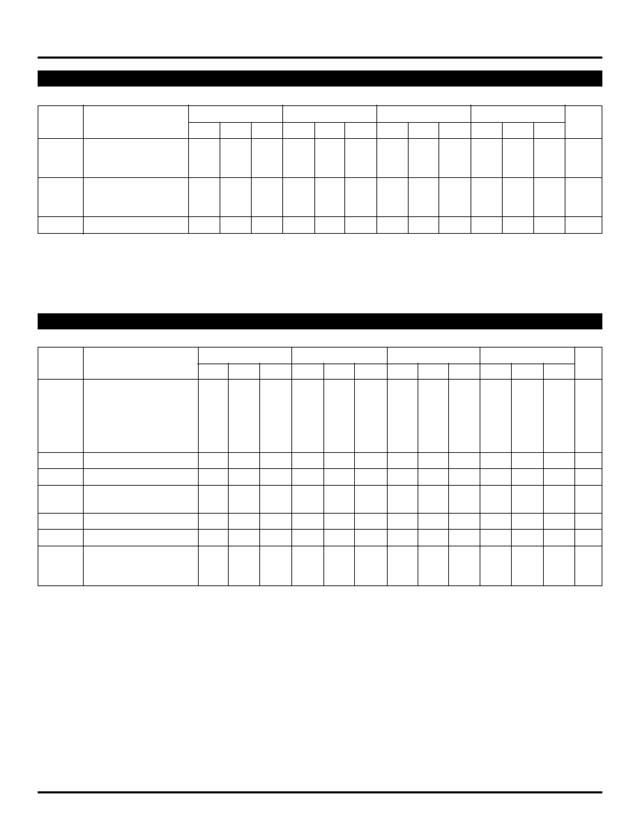
4
SY10EL16VA-VF
SY100EL16VA-VF
Micrel
T
A =
�40
�
C
T
A =
0
�
C
T
A =
+25
�
C
T
A =
+85
�
C
Symbol
Parameter
Min.
Typ.
Max.
Min.
Typ.
Max.
Min.
Typ.
Max.
Min.
Typ.
Max. Unit
t
PLH
Propagation Delay to
ps
t
PHL
Q, /Q Output
D (Diff)
--
--
350
--
--
350
--
--
350
--
--
380
D (SE)
--
--
400
--
--
400
--
--
400
--
--
430
Q
HG
, /Q
HG
Output
D (Diff)
--
--
650
--
--
650
--
--
650
--
--
730
D (SE)
--
--
700
--
--
700
--
--
700
--
--
780
t
S
Setup Time
/EN
--
150
--
--
150
--
--
150
--
--
150
--
ps
t
H
Hold Time
/EN
--
150
--
--
150
--
--
150
--
--
150
--
ps
t
skew
Duty Cycle Skew
(1)
(Diff)
--
5
--
--
5
20
--
5
20
--
5
20
ps
V
PP
Minimum Input Swing
(2)
150
--
--
150
--
--
150
--
--
150
--
--
mV
V
CMR
Common Mode Range
(3)
�1.3
--
�0.4
�1.4
--
�0.4
�1.4
--
�0.4
�1.4
--
�0.4
V
tr
Output Q
100
225
350
100
225
350
100
225
350
100
225
350
ps
tf
Rise/Fall Time
(20% TO 80%)
DC ELECTRICAL CHARACTERISTICS
(1)
T
A =
�40
�
C
T
A =
0
�
C
T
A =
+25
�
C
T
A =
+85
�
C
Symbol
Parameter
Min.
Typ.
Max.
Min.
Typ.
Max.
Min.
Typ.
Max.
Min.
Typ.
Max.
Unit
I
EE
Power Supply
mA
Current
10EL
--
--
40
--
--
40
--
--
40
--
--
40
100EL
--
--
40
--
--
40
--
--
40
--
--
46
V
BB
Output Reference
V
Voltage
10EL
�1.43
--
�1.30 �1.38
--
�1.27 �1.35
--
�1.25 �1.31
--
�1.19
100EL
�1.38
--
�1.26 �1.38
--
�1.26 �1.38
--
�1.26 �1.38
--
�1.26
I
IH
Input HIGH Current
--
--
150
--
--
150
--
--
150
--
--
150
�
A
V
EE
= V
EE
(Min) to V
EE
(Max), V
CC
= GND
NOTE:
1. Parametric values specified at:
10/100EL16VA-VF Series:
-3.0V to -5.5V.
NOTES:
1. Duty cycle skew is the difference between a t
PLH
and t
PHL
propagation delay through a device.
2. Minimum input swing for which AC parameters are guaranteed. The device has a DC gain of
40 to Q, /Q outputs and a DC gain of
200 or higher to
/Q
HG
/Q
HG
outputs.
3. The CMR range is referenced to the most positive side of the differential input signal. Normal operation is obtained if the HIGH level falls within the specified
range and the peak-to-peak voltage lies between V
PP
min. and 1V. The lower end of the CMR range varies 1:1 with V
EE
. The numbers in the spec table
assume a nominal V
EE
= �3.3V. Note for PECL operation, the V
CMR
(min) will be fixed at 3.3V � |V
CMR
(min)|.
4. Parametric values specified at:
10/100EL16VA-VF Series:
-3.0V to -5.5V.
AC ELECTRICAL CHARACTERISTICS
(4)
V
EE
= V
EE
(Min) to V
EE
(Max), V
CC
= GND

