
DESCRIPTION
I Accepts any differential input signal and provides
four LVDS output copies
I Guaranteed AC performance over temperature
and voltage:
∑ > 2.0GHz f
MAX
∑ < 20ps within-device skew
∑ < 190ps rise/fall times
I Low jitter design
∑ < 1ps(rms) cycle-to-cycle jitter
∑ < 10ps(pk-pk) total jitter
I 3.3V power supply operation
I TTL/CMOS input for enable
I Unique input termination and V
T
pin accepts DC-
coupled and AC-coupled inputs (CML, PECL, LVDS,
and HSTL)
I High-speed LVDS outputs
I Wide operating temperature range: ≠40
∞
C to +85
∞
C
I Available in 16-pin (3mm ◊ 3mm) MLFTM package
FEATURES
3.3V, 2GHz ANY-DIFFERENTIAL
INPUT-TO-LVDS 1:4 FANOUT BUFFER/
TRANSLATOR W/ INTERNAL TERMINATION
Precision EdgeTM
SY89833L
FINAL
APPLICATIONS
I Processor clock distribution
I SONET clock distribution
I Fibre Channel clock distribution
I Gigabit Ethernet clock distribution
1
Rev.: D
Amendment: /0
Issue Date:
February 2003
The SY89833L is a 3.3V, high-speed 2GHz differential
Low Voltage Differential Swing (LVDS) 1:4 fanout buffer
optimized for ultra-low skew applications. Within device skew
is guaranteed to be less than 20ps over supply voltage and
temperature.
The differential input buffer has a unique internal
termination design that allows access to the termination
network through a V
T
pin. This feature allows the device to
easily interface to different logic standards. A V
REF_AC
reference is included for AC-coupled applications.
The SY89833L is part of Micrel's high-speed clock
synchronization family. For 2.5V applications, the SY89832U
provides similar functionality while operating from a 2.5V
±5% supply. For applications that require a different I/O
combination, consult the Micrel website at
www.micrel.com,
and choose from a comprehensive product line of high-
speed, low-skew fanout buffers, translators and clock
generators.
FUNCTIONAL BLOCK DIAGRAM
TYPICAL PERFORMANCE
Precision Edge is a trademark of Micrel, Inc.
MicroLeadFrame and MLF are trademarks of Amkor Technology, Inc.
622MHz Output
TIME (321.9ps/div.)
≠
15mV Offset
(50mV/div
.)
IN
/IN
D
Q
Q3
/Q3
Q2
/Q2
Q1
/Q1
Q0
/Q0
EN
V
T
50
50
V
REF--AC
Precision EdgeTM

2
Precision EdgeTM
SY89833L
Micrel
PACKAGE/ORDERING INFORMATION
Ordering Information
Package
Operating
Package
Part Number
Type
Range
Marking
SY89833LMI
MLF-16
Industrial
833L
SY89833LMITR*
MLF-16
Industrial
833L
*Tape and Reel
Pin Number
Pin Name
Pin Function
15, 16,
(Q0, /Q0)
LVDS Differential (Outputs): Normally terminated with 100
across the pair (Q, /Q). See
1, 2, 3, 4, 5, 6
to
"LVDS Outputs" section, Figure 2a. Unused outputs should be terminated with a 100
(Q3, /Q3)
resistor across each pair.
8
EN
TTL/CMOS Compatible Synchronous Enable: When EN goes LOW, Q outputs will go
LOW and /Q outputs will go HIGH on the next LOW transition at IN inputs. Input threshold
is V
CC
/2V. A 25k
pull-up resistor is included. The default state is HIGH when left floating.
The internal latch is clocked on the falling edge of the input signal (IN, /IN).
9, 12
/IN, IN
Differential Clock (Inputs): Internal 50
termination resistors to the V
T
pin.
See
"Input Interface Applications" section.
10
VREF≠AC
Reference Voltages: Equals to V
CC
≠1.4V, and is used for AC-coupled applications.
The maximum sink/source current is 0.5mA. See
"Input Interface Applications."
When using V
REF≠AC
, bypass with a 0.01
µF capacitor to V
CC
.
11
VT
Termination Center-Tap. For CML or LVDS inputs, leave this pin floating. See Figures
3a to 3f. See
"LVDS Outputs" Figures 2a and 2b for LVDS differential and common
mode measurements.
13,
GND
Ground. Exposed pad internally connected to GND and must be connected to a ground
Exposed Pad
plane for proper thermal operation.
7, 14
VCC
Positive Power Supply: Bypass with 0.1
µF//0.01µF low ESR capacitors.
PIN DESCRIPTION
1
2
3
4
12
11
10
9
16 15 14 13
5
6
7
8
Q1
/Q1
Q2
/Q2
IN
VT
VREF--AC
/IN
GND
VCC
Q0
/Q0
EN
VCC
/Q3
Q3
16-Pin MLFTM
IN
/IN
EN
Q
/Q
0
1
1
0
1
1
0
1
1
0
X
X
0
0
(1)
1
(1)
Note 1.
On next negative transition of the input signal (IN).
TRUTH TABLE

3
Precision EdgeTM
SY89833L
Micrel
Absolute Maximum Ratings
(Note 1)
Supply Voltage (V
CC
) .................................. ≠0.5V to +4.0V
Input Voltage (V
IN
) ............................... ≠0.5V to V
CC
+0.3V
Output Current (I
OUT
) ...............................................
±10mA
Input Current (IN, /IN) ...............................................
±50mA
V
T
Current (I
VT
) ......................................................
±100mA
Input Sink/Source Current (V
REF≠AC
), Note 3 ............
±2mA
Lead Temperature (Soldering, 10 sec.) .................... 220
∞C
Storage Temperature (T
S
) ....................... ≠65
∞C to +150∞C
Operating Ratings
(Note 2)
Supply Voltage Range ............................ +2.97V to +3.63V
Ambient Temperature (T
A
) ......................... ≠40
∞C to +85∞C
Package Thermal Resistance
MLFTM
(
JA
)
Still-Air ............................................................. 60
∞C/W
500lfpm ............................................................ 54
∞C/W
MLFTM
(
JB
), Note 4 ........................................... 32
∞C/W
T
A
= ≠40
∞C to +85∞C
Symbol
Parameter
Condition
Min
Typ
Max
Units
V
CC
Power Supply Voltage Range
2.97
3.3
3.63
V
I
CC
Power Supply Current
No Load
75
100
mA
R
IN
Differential Input Resistance
80
100
120
(IN, /IN)
V
IH
Input HIGH Voltage
Note 3
0.1
V
CC
+0.3
V
(IN, /IN)
V
IL
Input LOW Voltage
Note 3
≠0.3
V
CC
+0.2
V
(IN, /IN)
V
IN
Input Voltage Swing
Note 3, see Figure 2c
0.1
3.6
V
V
IN
(max), V
T
= floating.
V
DIFF_IN
Differential Input Voltage
Note 3, see Figure 2d
0.2
V
|I
IN
|
Input Current
Note 3
45
mA
(IN, /IN)
V
REF≠AC
Reference Voltage
Note 3
V
CC
≠1.525 V
CC
≠1.425 V
CC
≠1.325
V
Note 1.
The circuit is designed to meet the DC specifications shown in the above table after thermal equilibrium has been established.
Note 2.
Specification for packaged product only.
Note 3.
Due to the internal termination (see
"Differential Input") the input current depends on the applied voltages at IN, /IN and V
T
inputs. Do not apply
a combination of voltages that causes the input current to exceed the maximum limit.
DC ELECTRICAL CHARACTERISTICS
(Note 1, 2)
Note 1.
Permanent device damage may occur if ABSOLUTE MAXIMUM RATINGS are exceeded. This is a stress rating only and functional operation is
not implied at conditions other than those detailed in the operational sections of this data sheet. Exposure to ABSOLUTE MAXIMUM RATlNG
conditions for extended periods may affect device reliability.
Note 2.
The data sheet limits are not guaranteed if the device is operated beyond the operating ratings.
Note 3.
Due to the limited drive capability use for input of the same package only.
Note 4.
Junction-to-board resistance assumes exposed pad is soldered (or equivalent) to the device's most negative potential on the PCB.

4
Precision EdgeTM
SY89833L
Micrel
V
CC
= 3.3V
±10%, T
A
= ≠40
∞C to +85∞C
Symbol
Parameter
Condition
Min
Typ
Max
Units
V
OH
Output HIGH Voltage
Note 3
1.475
V
V
OL
Output LOW Voltage
Note 3
0.925
V
V
OCM
Output Common Mode Voltage
1.125
1.275
V
V
OCM
Change in Common Mode Voltage
≠50
50
mV
V
OUT
Single-Ended Output
see Figures 2c-2d
250
350
450
mV
V
DIFF_OUT
Differential Output
see Figures 2c-2d
500
700
900
mV
Note 1.
The circuit is designed to meet the DC specifications shown in the above table after thermal equilibrium has been established.
Note 2.
Specification for packaged product only.
Note 3.
Measured as per Figure 2a, 100
across Q and /Q outputs.
V
CC
= 3.3V
±10%, T
A
= ≠40
∞C to +85∞C
Symbol
Parameter
Condition
Min
Typ
Max
Units
V
IH
Input HIGH Voltage
2.0
V
CC
V
V
IL
Input LOW Voltage
0
0.8
V
I
IH
Input HIGH Current
≠125
20
µA
I
IL
Input LOW Current
≠300
µA
Note 1.
The circuit is designed to meet the DC specifications shown in the above table after thermal equilibrium has been established.
Note 2.
Specification for packaged product only.
LVDS OUTPUTS DC ELECTRICAL CHARACTERISTICS
(Note 1, 2)
LVTTL/CMOS INPUTS DC ELECTRICAL CHARACTERISTICS
(Note 1, 2)

5
Precision EdgeTM
SY89833L
Micrel
V
CC
= 3.3V
±10%, T
A
= ≠40
∞C to +85∞C
Symbol
Parameter
Condition
Min
Typ
Max
Units
f
MAX
Maximum Frequency
200mVpp Output Swing
2.0
GHz
t
PLH
Differential Propagation
Input Swing: <400mV
400
500
600
ps
t
PHL
(Delay) (IN-to-Q)
Input Swing:
400V
330
440
530
ps
t
SKEW
Within-Device Skew (Differential)
Note 3
5
20
ps
Part-to-Part Skew (Differential)
200
ps
t
S
Set-Up Time (EN to IN, /IN)
Note 4 and Note 5
300
ps
t
H
Hold Time (EN to IN, /IN)
Note 4 and Note 5
500
ps
t
JITTER
Cycle-to-Cycle Jitter (rms)
Note 6
1
ps(rms)
Total Jitter
Note 7
10
ps(pk-pk)
t
r
,
t
f
Output Rise/Fall Times
60
110
190
ps
(20% to 80%)
Note 1.
Measured with 400mV input signal, 50% duty cycle, all outputs are loaded with 100
between Q and /Q. Output swing is 200mV.
Note 2.
Specification for packaged product only.
Note 3.
Skew is measured between outputs under identical transitions.
Note 4.
Set-up and hold times apply to synchronous applications that intend to enable/disable before the next clock cycle. For asynchronous applica-
tions set-up and hold times do not apply.
Note 5.
See
"Timing Diagram."
Note 6.
Cycle-to-cycle jitter definition: The variation period between adjacent cycles over a random sample of adjacent cycle pairs.
T
JITTER_CC
= T
n
≠T
n+1
where T is the time between rising edges of the output signal.
Note 7.
Total jitter definition: with an ideal clock input frequency of
f
MAX
(device), no more than one output edge in 10
12
output edges will deviate by more
than the specified peak-to-peak jitter value.
AC ELECTRICAL CHARACTERISTICS
(Note 1, 2)
TIMING DIAGRAM
t
S
IN
/Q
Q
t
PLH
,
t
PHL
t
H
EN
V
CC
/2
V
CC
/2
t
PLH
,t
PHL
V
IN
V
OUT
Swing
/IN

6
Precision EdgeTM
SY89833L
Micrel
TYPICAL OPERATING CHARACTERISTICS
0
100
200
300
400
500
600
0
200
400
600
800
PROPAGATION DELAY (ps)
INPUT VOLTAGE SWING (mV)
Propagation Delay
vs. Input Voltage Swing
0
2
4
6
8
10
12
14
-40 -20
0
20
40
60
80 100
T
SKEW
(ps)
TEMPERATURE (
∞C)
T
SKEW
vs. Temperature
0
50
100
150
200
250
300
350
0
0.5
1
1.5
2
2.5
AMPLITUDE (mV)
FREQUENCY (GHz)
Output Swing
vs. Frequency
V
CC
= 3.3V, V
IN
= 400mV, T
A
= 25
∞C, unless otherwise stated.

7
Precision EdgeTM
SY89833L
Micrel
155MHz Output
TIME (1.29ns/div.)
--
15mV Of
fset
(150mV/div
.)
FUNCTIONAL CHARACTERISTICS
622MHz Output
TIME (321.9ps/div.)
--
15mV Of
fset
(150mV/div
.)
1GHz Output
TIME (200ps/div.)
--
10mV Of
fset
(150mV/div
.)
V
CC
= 3.3V, V
IN
= 400mV, T
A
= 25
∞C, unless otherwise stated.

8
Precision EdgeTM
SY89833L
Micrel
INPUT STAGE
1.86k9
GND
V
CC
/IN
1.86k9
509
1.86k9
1.86k9
IN
V
T
509
Figure 1a. Simplified Differential Input Buffer
R
25k
GND
EN
V
CC
V
CC
R
Figure 1b. Simplified TTL/CMOS Input Buffer
LVDS OUTPUTS
LVDS specifies a small swing of 350mV typical, on a
nominal 1.25V common mode above ground. The common
100
GND
v
OUT
v
OH
, v
OL
v
OH
, v
OL
Figure 2a. LVDS Differential Measurement
Q
OUT
/Q
OUT
V
OUT,
V
IN
350mV
(typical)
Figure 2c. Single-Ended Swing
50
GND
v
OCM
,
v
OCM
50
Figure 2b. LVDS Common Mode Measurement
Q
OUT
/Q
OUT
700mV
Q
OUT
≠
/Q
OUT
V
DIFF_IN,
V
DIFF_OUT
Figure 2d. Differential Swing
mode voltage has tight limits to permit large variations in
ground noise between an LVDS driver and receiver.
9
Precision EdgeTM
SY89833L
Micrel
RELATED PRODUCT AND SUPPORT DOCUMENTS
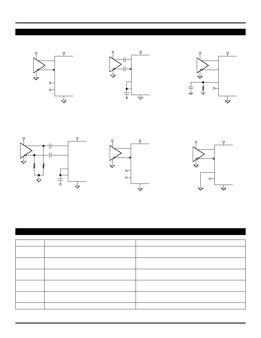
INPUT INTERFACE APPLICATIONS
NC
CML
IN
/IN
VT
NC
SY89833L
V
CC
= 3.3V
V
CC
= 3.3V
VREF_AC
Figure 3a. DC-Coupled CML
Input Interface
CML
IN
/IN
VT
V
CC
V
CC
= 3.3V
V
CC
SY89833L
VREF_AC
0.01
µF
Figure 3b. AC-Coupled CML
Input Interface
LVPECL
IN
/IN
VT
V
CC
= 3.3V
V
CC
= 3.3V
SY89833L
VREF_AC
V
CC
≠2V*
NC
50
0.01
µF
Figure 3c. DC-Coupled PECL
Input Interface
IN
/IN
VT
Rpd
100
Rpd
100
V
CC
= 3.3V
V
CC
= 3.3V
SY89833L
VREF_AC
V
CC
0.01
µF
LVPECL
Figure 3d. AC-Coupled PECL
Input Interface
NC
LVDS
IN
/IN
VT
NC
SY89833L
V
CC
V
CC
= 3.3V
VREF_AC
Figure 3e. LVDS
Input Interface
HSTL
IN
/IN
VT
V
CC
= 1.8V to 3.3V
V
CC
= 3.3V
SY89833L
VREF_AC
NC
Figure 3f. HSTL
Input Interface
Part Number
Function
Data Sheet Link
SY89830U
2.5V/3.3V/5V 2.5GHz 1:4 PECL/ECL
Clock Driver with 2:1 Differential Input Mux
http://www.micrel.com/product-info/products/sy89830u.shtml
SY89831U
2GHz Ultra Low-Jitter and Skew 1:4 LVPECL
Fanout Buffer/Translator w/ Internal Termination
http://www.micrel.com/product-info/products/sy89831u.shtml
SY89832U
2GHz Ultra Low-Jitter and Skew 1:4 LVPECL
Fanout Buffer/Translator w/ Internal Termination
http://www.micrel.com/product-info/products/sy89832u.shtml
SY89833U
2GHz ANY DIFFERENTIAL INPUT-to-LVDS Out
1:4 Fanout Buffer Translator w/ Internal Termination
http://www.micrel.com/product-info/products/sy89833u.shtml
16-MLFTM Manufacturing Guidelines
Exposed Pad Application Note
http://www.amkor.com/products/notes_papers/MLF_appnote_0301.pdf
HBW Solutions
New Products and Termination App. Note
http://www.micrel.com/product-info/as/solutions.shtml
(*Bypass with 0.01
µF to GND)

10
Precision EdgeTM
SY89833L
Micrel
16 LEAD EPAD
MicroLeadFrameTM (MLF-16)
Package
EP- Exposed Pad
Die
CompSide Island
Heat Dissipation
Heavy Copper Plane
Heavy Copper Plane
V
EE
V
EE
Heat Dissipation
PCB Thermal Consideration for 16-Pin MLFTM Package
(Always solder, or equivalent, the exposed pad to the PCB)
3.00BSC
2.75BSC
0.50 DIA
3.00BSC
12
∞ max
SEATING
PLANE
2.75BSC
16
1
1
2
3
4
N
2
3
4
0.85
+0.15
≠0.65
0.65
+0.15
≠0.65
0.01
+0.04
≠0.01
0.23
+0.07
≠0.05
0.01
+0.04
≠0.01
0.42
+0.18
≠0.18
0.42
+0.18
≠0.18
0.23
+0.07
≠0.05
1.60
+0.10
≠0.10
PIN 1 ID
0.5 BSC
1.5 REF
0.42
+0.18
≠0.18
1.60
+0.10
≠0.10
0.40
+0.05
≠0.05
0.20 REF.
0.5BSC
SECTION "C-C"
SCALE: NONE
FOR EVEN TERMINAL/SIDE
TOP VIEW
BOTTOM VIEW
1. DIMENSIONS ARE IN mm.
2. DIE THICKNESS ALLOWABLE IS 0.305mm MAX.
3. PACKAGE WARPAGE MAX 0.05mm.
4. THIS DIMENSION APPLIES TO PLATED TERMINAL AND IS MEASURED
BETWEEN 0.20mm AND 0.25mm FROM TIP.
5. APPLIES ONLY FOR TERMINALS
C C
CL
4
Rev. 02
Package Notes:
Note 1.
Package meets Level 2 moisture sensitivity classification, and are shipped in dry-pack form.
Note 2.
Exposed pads must be soldered to a ground for proper thermal management.
MICREL, INC.
1849 FORTUNE DRIVE
SAN JOSE, CA 95131
USA
TEL
+ 1 (408) 944-0800
FAX
+ 1 (408) 944-0970
WEB
http://www.micrel.com
The information furnished by Micrel in this datasheet is believed to be accurate and reliable. However, no responsibility is assumed by Micrel for its use.
Micrel reserves the right to change circuitry and specifications at any time without notification to the customer.
Micrel Products are not designed or authorized for use as components in life support appliances, devices or systems where malfunction of a product can
reasonably be expected to result in personal injury. Life support devices or systems are devices or systems that (a) are intended for surgical implant into
the body or (b) support or sustain life, and whose failure to perform can be reasonably expected to result in a significant injury to the user. A Purchaser's
use or sale of Micrel Products for use in life support appliances, devices or systems is at Purchaser's own risk and Purchaser agrees to fully indemnify
Micrel for any damages resulting from such use or sale.
© 2003 Micrel, Incorporated.