May 1997
ML2258
*
µP Compatible 8-Bit A/D Converter
with 8-Channel Multiplexer
1
GENERAL DESCRIPTION
The ML2258 combines an 8-bit A/D converter, 8-channel
analog multiplexer, and a microprocessor compatible 8-
bit parallel interface and control logic in a single
monolithic device.
Easy interface to microprocessors is provided by the
latched and decoded multiplexer address inputs and
latched three-state outputs.
The device is suitable for a wide range of applications
from process and machine control to consumer,
automotive, and telecommunication applications.
The ML2258 is an enhanced, pin-compatible, second
source for the industry standard ADC0808/ADC0809. The
ML2258 enhancements are faster conversion time, true
sample and hold function, superior power supply
rejection, wider reference range, and a double buffered
data bus as well as faster digital timing. All parameters
are guaranteed over temperature with a power supply
voltage of 5V ±10%.
FEATURES
s
Conversion time
6.6µs
s
Total unadjusted error
±1/2LSB or ±1LSB
s
No missing codes
s
Sample and hold
390ns acquisition
s
Capable of digitizing a 5V, 50kHz sine wave
s
8-input multiplexer
s
0V to 5V analog input range with single 5V
power supply
s
Operates ratiometrically or with up to 5V
voltage reference
s
No zero-or full-scale adjust required
s
Analog input protection
25mA per input min
s
Low power dissipation
3mA max
s
TTL and CMOS compatible digital inputs and outputs
s
Standard 28-pin DIP or surface mount PCC
s
Superior pin compatible replacement for ADC0808 and
ADC0809
* Some Packages Are End Of Life As Of August 1, 2000
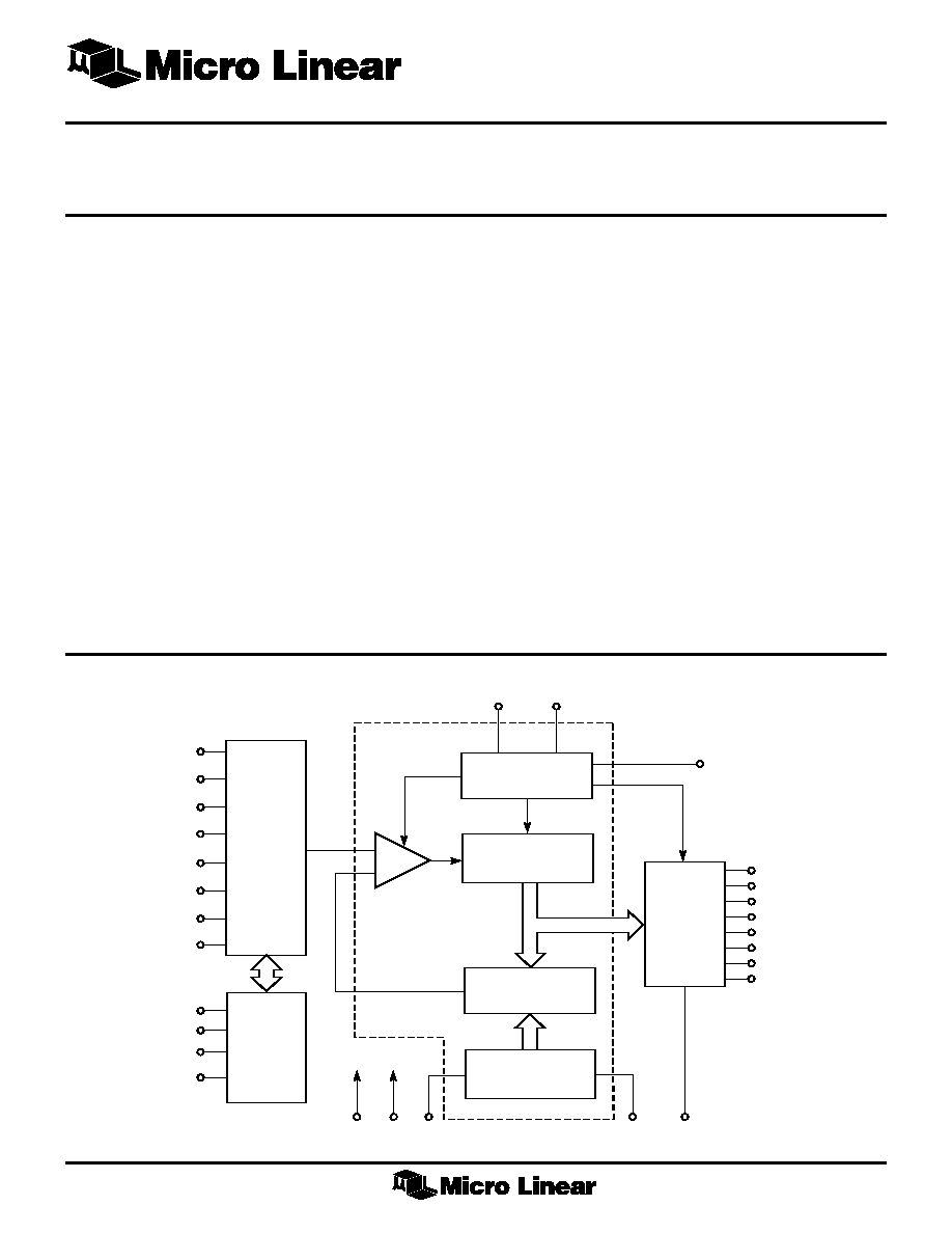
BLOCK DIAGRAM
COMPARATOR
A/D WITH
SAMPLE HOLD
CONTROL & TIMING
S.A.R.
SWITCH TREE
THREE
STATE
OUTPUT
LATCH
BUFFER
DB0
DB1
DB2
DB3
DB4
DB5
DB6
DB7
OUTPUT
ENABLE
≠V
REF
+V
REF
GND
V
CC
CAPACITOR/
RESISTOR
ARRAY
ADDRESS
LATCH
AND
DECODER
ADDR0
ADDR1
ADDR2
ADDRESS
LATCH ENABLE
IN7
IN6
IN0
IN1
IN2
IN3
IN4
IN5
8-CHANNEL
MULTIPLEXER
START
CLOCK
END OF CONVERSION
(INTERRUPT)

ML2258
2
PIN CONFIGURATION
ML2258
28-Pin DIP (P28)
ML2258
28-Pin PCC (Q28)
IN3
IN4
IN5
IN6
IN7
START
EOC
DB3
OE
CLK
V
CC
+V
REF
GND
DB1
IN2
IN1
IN0
ADDR0
ADDR1
ADDR2
ALE
DB7
DB6
DB5
DB4
DB0
≠V
REF
DB2
1
2
3
4
5
6
7
8
9
10
11
12
13
14
28
27
26
25
24
23
22
21
20
19
18
17
16
15
TOP VIEW
PIN DESCRIPTION
PIN# NAME
FUNCTION
1
IN3
Analog input 3.
2
IN4
Analog input 4.
3
IN5
Analog input 5.
4
IN6
Analog input 6.
5
IN7
Analog input 7.
6
START
Start of conversion. Active high digital
input pulse initiates conversion.
7
EOC
End of conversion. This output goes
low after a START pulse occurs, stays
low for the entire A/D conversion, and
goes high after conversion is
completed. Data on DB0≠DB7 is valid
on rising edge of EOC and stays valid
until next EOC rising edge.
8
DB3
Data output 3.
9
OE
Output enable input. When OE = 0,
DB0≠DB7 are in high impedance
state; OE = 1, DB0≠DB7 are active
outputs.
10 CLK
Clock. Clock input provides timing for
A/D converter, S/H, and digital
interface.
11 V
CC
Positive supply. 5V ± 10%.
12 +V
REF
Positive reference voltage.
PIN# NAME
FUNCTION
13
GND
Ground. 0V, all analog and digital
inputs or outputs are reference to this
point.
14
DB1
Data output 1.
15
DB2
Data output 2.
16
≠V
REF
Negative reference voltage.
17
DB0
Data output 0.
18
DB4
Data output 4.
19
DB5
Data output 5.
20
DB6
Data output 6.
21
DB7
Data output 7.
22
ALE
Address latch enable. Input to latch in
the digital address (ADDR2≠0) on the
rising edge of the multiplexer.
23
ADDR0
Address input 0 to multiplexer. Digital
input for selecting analog input.
24
ADDR1
Address input 1 to multiplexer. Digital
input for selecting analog input.
25
ADDR2
Address input 2 to multiplexer. Digital
input for selecting analog input.
26
IN0
Analog input 0.
27
IN1
Analog input 1.
28
IN2
Analog input 2.
ADDR0
ADDR1
ADDR2
ALE
DB7
DB6
DB5
IN7
START
EOC
DB3
OE
CLK
V
CC
12
13 14
15
16
IN6
IN5
IN4
IN3
IN2
IN1
IN0
+V
REF
GND
DB1
DB2
≠V
REF
DB0
DB4
17
18
5
6
7
8
9
10
11
4
3
2
1
28
25
24
23
22
21
20
19
27
26
TOP VIEW

ML2258
3
ELECTRICAL CHARACTERISTICS
Unless otherwise specified, T
A
= T
MIN
to T
MAX
, V
CC
= +V
REF
= 5V ±10%, ≠V
REF
= GND and f
CLK
= 10.24MHz
ML2258B
ML2258C
TYP
TYP
PARAMETER
NOTES
CONDITIONS
MIN
(NOTE 4)
MAX
MIN
(NOTE 4)
MAX
UNITS
Converter and Multiplexer
Total Unadjusted Error
5, 7
V
REF
= V
CC
±1/2
±1
LSB
+V
REF
Voltage Range
6
≠V
REF
V
CC
+ 0.1
≠V
REF
V
CC
+ 0.1
V
≠V
REF
Voltage Range
6
GND ≠ 0.1
+V
REF
GND ≠ 0.1
+V
REF
V
Reference Input Resistance
5
14
20
28
14
20
28
k ˝
Analog Input Range
5, 8
GND ≠ 0.1
V
CC
+ 0.1 GND ≠ 0.1
V
CC
+ 0.1
V
Power Supply Sensitivity
6
DC, V
CC
= 5V ± 10%
±1/32
±1/4
±1/32
±1/4
LSB
100mVp-p, 100kHz
±1/16
±1/16
LSB
sine on V
CC
, V
IN
= 0
I
OFF
, Off Channel Leakage
5, 9
On Channel = V
CC
≠1
≠1
µA
Current (Note 9)
Off Channel = 0V
On Channel = 0V
1
1
µA
Off Channel = V
CC
I
ON
, On Channel Leakage
5, 9
On Channel = 0V
≠1
≠1
µA
Current (Note 9)
Off Channel = V
CC
On Channel = V
CC
1
1
µA
Off Channel = 0V
Digital and DC
V
IN(1)
, Logical "1" Input
5
2.0
2.0
V
Voltage
V
IN(0)
, Logical "0" Input
5
0.8
0.8
V
Voltage
I
IN(1)
, Logical "1" Input
5
V
IN
= V
CC
1
1
µA
Current
I
IN(0)
, Logical "0" Input
5
V
IN
= 0V
≠1
≠1
µA
Current
V
OUT(1)
, Logical "1"
5
I
OUT
= ≠2mA
4.0
4.0
V
Output Voltage
V
OUT(0)
, Logical "0"
5
I
OUT
= 2mA
0.4
0.4
V
Output Voltage
I
OUT
, Three-State Output
5
V
OUT
= 0V
≠1
≠1
µA
Current
V
OUT
= V
CC
1
1
µA
I
CC
, Supply Current
5
1.5
3
1.5
3
mA
ABSOLUTE MAXIMUM RATINGS
(Note 1)
Supply Voltage, V
CC ..............................................................
6.5V
Voltage
Logic Inputs .................................. ≠0.3V to V
CC
+0.3V
Analog Inputs ............................... ≠0.3V to V
CC
+0.3V
Input Current per Pin (Note 2) .............................. ±25mA
Storage Temperature .............................. ≠65∞C to +150∞C
Package Dissipation
at T
A
= 25∞C (Board Mount) ............................. 875mW
Lead Temperature (Soldering 10 sec.)
Dual-In-Line Package (Plastic) ............................ 260∞C
Molded Chip Carrier Package
Vapor Phase (60 sec.) ..................................... 215∞C
Infrared (15 sec.) ............................................ 220∞C
OPERATING CONDITIONS
Supply Voltage, V
CC ....................................
4.5V
DC
to 6.3V
DC
Temperature Range (Note 3) ................. T
MIN
- T
A
- T
MAX
ML2258BIP, ML2258BIQ, ML2258CIP,
ML2258CIQ ........................................ ≠40∞C to +85∞C

ML2258
4
ELECTRICAL CHARACTERISTICS
(Continued)
TYP
SYMBOL
PARAMETER
NOTES
CONDITIONS
MIN (NOTE 4)
MAX
UNITS
AC and Dynamic Performance Characteristics (Note 10)
t
ACQ
Sample and Hold Acquisition
4
1/f
CLK
f
CLK
Clock Frequency
5
100
10240
kHz
t
C
Conversion Time
5
67
67 + 250ns 1/f
CLK
SNR
Signal to Noise Ratio
V
IN
= 51kHz, 5V sine.
47
dB
f
CLK
= 10.24MHz
(f
SAMPLING
> 150kHz). Noise is sum
of all nonfundamental components
up to 1/2 of f
SAMPLING
THD
Total Harmonic Distortion
V
IN
= 51kHz, 5V sine.
≠60
dB
f
CLK
= 10.24MHz
(f
SAMPLING
> 150kHz). THD is sum
of 2, 3, 4, 5 harmonics relative to
fundamental
IMD
Intermodulation Distortion
V
IN
= f
A
+ f
B
. f
A
= 49kHz, 2.5V sine.
≠60
dB
f
B
= 47.8kHz, 2.5V sine,
f
CLK
= 10.24MHz
(f
SAMPLING
> 150kHz). IMD is (f
A
+ f
B
),
(f
A
≠ f
B
), (2f
A
+ f
B
), (2f
A
≠ f
B
), (f
A
+ 2f
B
),
(f
A
≠ 2f
B
) relative to fundamental
FR
Frequency Response
V
IN
= 0 to 50kHz. 5V sine relative
0.1
dB
to 1kHz
t
DC
Clock Duty Cycle
6, 11
40
60
%
t
EOC
End of Conversion Delay
5
8
8 + 250ns
1/f
CLK
t
WS
Start Pulse Width
5
50
ns
t
SS
Start Pulse Setup Time
6, 12
Synchronous only
40
ns
t
WALE
Address Latch Enable Pulse Width
5
50
ns
t
S
Address Setup
5
0
ns
t
H
Address Hold
5
50
ns
t
H1, H0
Output Enable for DB0≠DB7
6
Figure 1, C
L
= 50pF
100
ns
6
Figure 1, C
L
= 10pF
50
ns
t
1H, 0H
Output Disable for DB0≠DB7
6
Figure 1, C
L
= 50pF
200
ns
6
Figure 1, C
L
= 10pF
100
ns
C
IN
Capacitance of Logic Input
5
pF
C
OUT
Capacitance of Logic Outputs
10
pF
Note 1: Absolute maximum ratings are limits beyond which the life of the integrated circuit may be impaired. All voltages unless otherwise specified are measured with
respect to ground.
Note 2: When the input voltage (V
IN
) at any pin exceeds the power supply rails (V
IN
< V≠ or V
IN
> V+) the absolute value of current at that pin should be limited to 25mA or less.
Note 3: ≠40∞C to +85∞C operating temperature range devices are 100% tested with temperature limits guaranteed by 100% testing, sampling, or by correlation with worst-
case test conditions.
Note 4: Typicals are parametric norm at 25∞C.
Note 5: Parameter guaranteed and 100% production tested.
Note 6: Parameter guaranteed. Parameters not 100% tested are not in outgoing quality level calculation.
Note 7: Total unadjusted error includes offset, full scale, linearity, multiplexer and sample and hold errors.
Note 8: For ≠V
REF
∑ V
IN
(+) the digital output code will be 0000 0000. Two on-chip diodes are tied to each analog input which will forward conduct for analog input voltages
one diode drop below ground or one diode drop greater than the V
CC
supply. Be careful, during testing at low V
CC
levels (4.5V), as high level analog inputs (5V) can
cause this input diode to conduct -- especially at elevated temperatures, and cause errors for analog inputs near full scale. The spec allow 100mV forward bias of either
diode. This means that as long as the analog V
IN
or V
REF
does not exceed the supply voltage by more than 100mV, the output code will be correct. To achieve an
absolute 0V
DC
to 5V
DC
input voltage range will therefore require a minimum supply voltage of 4.900V
DC
over temperature variations, initial tolerance and loading.
Note 9: Leakage current is measured with the clock not switching.
Note 10: C
L
= 50pF, timing measured at 50% point.
Note 11: A 40% to 60% clock duty cycle range insures proper operation at all clock frequencies. In the case that an available clock has a duty cycle outside of these limits,
the minimum time the clock is high or the minimum time the clock is low must be at least 40ns. The maximum time the clock can be high or low is 60µs.
Note 12: The conversion start setup time requirement only needs to be satisfied if a conversion must be synchronized to a given clock rising edge. If the setup time is not met,
start conversion will have an uncertainty of one clock pulse.

ML2258
5
DATA
OUTPUT
C
L
10K
t
1H
,t
H1
DATA
OUTPUT
C
L
10K
t
0H
,t
H0
V
CC
V
CC
GND
V
OH
GND
50%
10%
t
f
t
1H
90%
90%
OUTPUT
ENABLE
OUTPUT
t
1H
,C
L
= 10pF
V
CC
GND
V
CC
V
OL
50%
10%
t
f
t
0H
90%
10%
OUTPUT
ENABLE
OUTPUT
t
0H
,C
L
= 10pF
t
H1
,C
L
= 50pF
t
r
t
0H
90%
50%
10%
50%
t
H0
,C
L
= 50pF
t
r
t
H0
90%
50%
10%
50%
Figure 1. High Impedance Test Circuits and Waveforms
TYPICAL PERFORMANCE CURVES
Figure 2. Linearity Error vs f
CLK
1.0
0.75
0.5
0.25
0
0.01
0.1
1.0
10
CLOCK FREQUENCY (MHz)
LINEARITY ERROR (LSB)
≠55 C
25 C
125 C
V
CC
= 5V
V
REF
= 5V