 | –≠–ª–µ–∫—Ç—Ä–æ–Ω–Ω—ã–π –∫–æ–º–ø–æ–Ω–µ–Ω—Ç: ML4423CS | –°–∫–∞—á–∞—Ç—å:  PDF PDF  ZIP ZIP |
July 2000
ML4423
*
1, 2, or 3-Phase Variable Speed AC Motor Controller
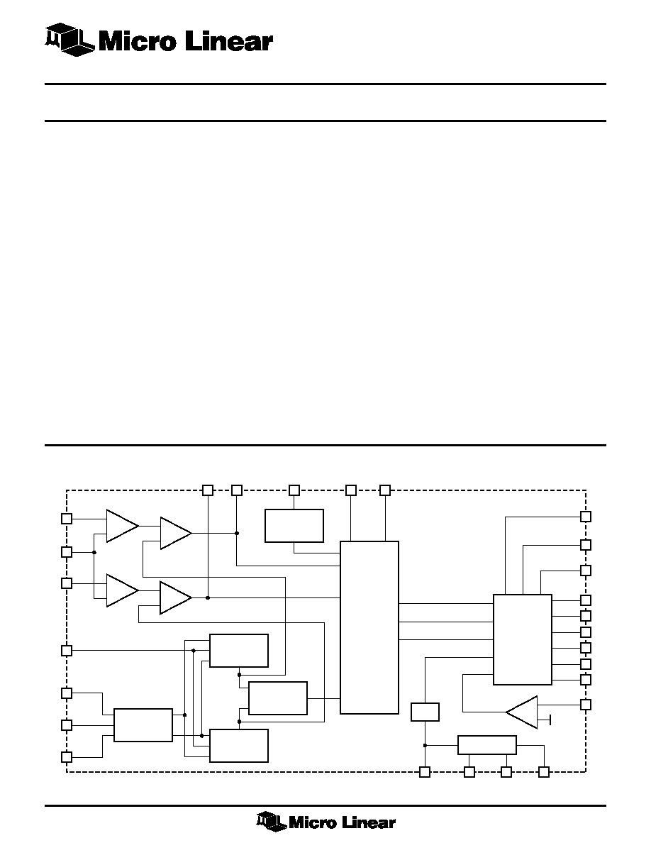
BLOCK DIAGRAM
1
GENERAL DESCRIPTION
The ML4423 provides the PWM sinewave drive signals
necessary for controlling three phase AC induction motors as
well as single and two phase split capacitor AC induction
motors.
A constant voltage/frequency ratio can be maintained
over a frequency range of greater than 10:1, providing
15Hz to 150Hz control. The output variable frequency AC
voltages are sensed and fed back to the controller to track the
sinewave frequency and amplitude set at the speed control
input. Direction, on two and three phase motors, is controlled
by changing the relative phase difference between the motor
windings: 90
◊ for two phase motors and 120◊ and 240◊ for three
phase motors.
To protect the motor, power devices, high voltage drivers
and control circuitry, the ML4423 includes fixed period,
pulse by pulse variable duty cycle current limit, deadtime
circuitry, and undervoltage lockout. The ML4423 has
selectable output voltage swing of 5V or 12V for
interfacing to different high side drivers and power devices.
FEATURES
s
Drives single, two, and three phase AC motors
s
Greater than 10:1 variable speed control range
s
Constant V/F ratio with programmable end points
s
Reverse capability for two and three phase motors
s
Low distortion PWM sinewave drive
s
Eliminates run capacitors in PSC motors
s
Coast function for quick power disable
s
Low cost interface for various gate drivers
s
PWM current limit, undervoltage lockout, and
programmable deadtime
s
12V
±20% operation with onboard 8V reference
(* Indicates Part Is End Of Life As Of July 1, 2000)
VSPEED
5
CO
12
FB A
1
RSPEED
6
VMIN
4
VDD
GND
RREF
REFERENCE
VREF
26
CT
17
8
7
HA
HB
HC
LA
LB
GATING
LOGIC
&
OUTPUT
DRIVERS
PWM
SINE
WAVE
CONTROL
PWM
OSCILLATOR
SINE A
GENERATOR
SINE C
GENERATOR
SPEED
CONTROL
SINE B
GENERATOR
UVLO
LC
20
ISENSE
16
19
21
23
22
24
5V/12 SELECT
25
RDT
9
COAST
14
13
SINE A-C
27
SINE B-C
28
3PH/2PH
18
F/
R
15
+
≠
COMP
0.5V
+
≠
+
≠
FB B
3
FB C
2
+
≠
+
≠
ML4423
2
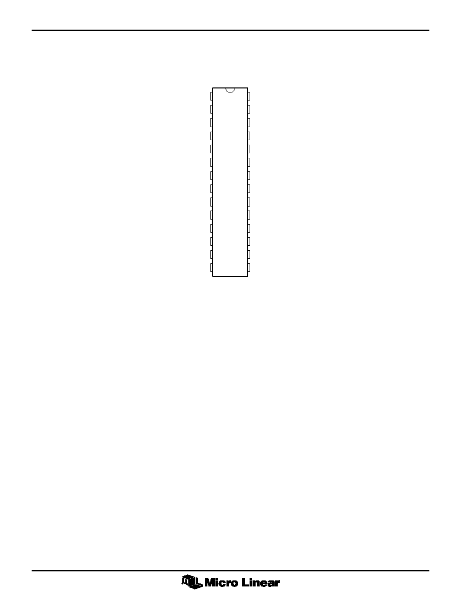
PIN CONFIGURATION
1
2
3
4
5
6
7
8
9
10
11
12
03
14
28
27
26
25
24
23
22
21
20
19
18
17
16
15
SENSE A
SENSE C
SENSE B
VMIN
VSPEED
RSPEED
VREF
RREF
RDT
SINE A-C
SINE B-C
CO
CT
COAST
CGM2
CGM1
VDD
5V/12V SELECT
HA
HC
HB
LA
LC
LB
3PH/2PH
GND
ISENSE
F/
R
TOP VIEW
ML4423
28-Pin Narrow PDIP (P28N)
28-Pin SOIC (S28)

ML4423
3
PIN DESCRIPTION
PIN
NAME
FUNCTION
1
FB A
Differential input which, in
conjunction with FB C, feeds back the
voltage applied across motor winding
A-C.
2
FB C
Input which feeds back the voltage
applied to motor winding C. Reference
voltage for windings A and B.
3
FB B
Differential input which, in
conjunction with FB C, feeds back the
voltage applied across motor winding
B-C.
4
V
MIN
The voltage on this pin sets the
minimum sinewave amplitude at low
speeds.
5
V
SPEED
The voltage on this pin sets the
frequency and amplitude of the
sinewaves generated at SINE
A
and
SINE
B
.
6
R
SPEED
An external resistor to ground provides
a variable current to the sinewave
generator. The current is proportional
to V
SPEED
.
7
V
REF
8V reference output which can be
used for setting V
SPEED
and V
MIN
.
8
R
REF
An external resistor to ground provides
a constant current used for setting the
PWM frequency in conjunction with
C
T
.
9
R
DT
An external resistor to ground sets the
deadtime in the output stage to
prevent cross-conduction in the power
devices.
10
SINE A-C
A test output for observing the
internally generated sinewave used for
motor winding A-C.
11
SINE B-C
A test output for observing the
internally generated sinewave used for
motor winding B-C.
12
C
O
An external capacitor to ground sets
the sinewave frequency in conjunction
with V
SPEED
and R
SPEED
.
PIN
NAME
FUNCTION
13
C
T
An external capacitor to ground sets
the PWM triangle frequency in
conjunction with the external resistor
R
REF
.
14
COAST
A logic low input causes all output
drive transistors to turn OFF. An
internal pull-up drives COAST to V
DD
if left unconnected.
15
F/R
A logic high input causes phase A to
lead phase B, while a logic low input
causes phase A to lag phase B. An
internal pull-up drives F/R to V
DD
if
left unconnected.
16
I
SENSE
Motor current sense input.
17
GND
Signal and power ground.
18
3PH/2PH
Leaving this pin unconnected selects
3-phase drive. Connecting this pin to
V
DD
selects single/2-phase drive.
19
LB
Low side drive output for phase B.
20
LC
Low side drive output for phase C.
21
LA
Low side drive output for phase A.
22
HB
High side drive output for phase B.
23
HC
High side drive output for phase C.
24
HA
High side drive output for phase A.
25
5V/12V
Input to select 5V or 12V output drive.
SELECT
Leaving this pin unconnected selects
5V output drive levels at the driver
outputs. Connecting this pin to V
CC
selects 12V output drive levels at the
driver outputs.
26
V
DD
12V power supply input.
27
C
GM1
An external capacitor to ground sets a
pole in the feedback loop.
28
C
GM2
An external capacitor to ground sets a
pole in the feedback loop.

ML4423
4
ABSOLUTE MAXIMUM RATINGS
Absolute maximum ratings are those values beyond which
the device could be permanently damaged. Absolute
maximum ratings are stress ratings only and functional
device operation is not implied.
V
DD ..............................................................................................
15V
Output Drive Current ...........................................
±50mA
Logic Inputs (F/R, COAST) .............................. ≠0.3 to 7V
Junction Temperature .............................................. 150∫C
Storage Temperature Range ...................... ≠65∫C to 150∫C
Lead Temperature (Soldering 10 sec) ...................... 260∫C
Thermal Resistance (
q
JA
)
Plastic DIP ....................................................... 52∫C/W
Plastic SOIC .................................................... 75∫C/W
OPERATING CONDITIONS
Temperature Range
C Suffix ...................................................... 0∫C to 70∫C
I Suffix .................................................... ≠40∫C to 85∫C
V
DD
........................................................... 9.6V to 14.4V
ELECTRICAL CHARACTERISTICS
Unless otherwise specified, V
DD
= 12V
± 20%, R
SPEED
= 160k
W, R
SENSE
= 250m
W, R
REF
= 200k
W,
C
0
= 0.47
mF, C
PWM
= 220pF, R
DT
= 166k
W, T
A
= Operating Temperature Range (Note 1).
SYMBOL
PARAMETER
CONDITIONS
MIN
TYP
MAX
UNITS
REFERENCE
V
REF
Output Voltage
7.6
7.8
8.2
V
Line Regulation
Total Variation
Line, Temperature
DIGITAL INPUTS
V
IL
Input Low Voltage
0.8
V
V
IH
Input High Voltage
2
V
OUTPUT DRIVERS
V
OL
Output Low Voltage
I
OL
= 20mA, 5V/12V SELECT = V
DD
1
V
I
OL
= 2mA, 5V/12V SELECT = open
0.1
V
V
OH
Output High Voltage
I
OL
= ≠20mA, 5V/12V SELECT = V
DD
V
DD
≠ 1
V
I
OL
= ≠2mA, 5V/12V SELECT = open
5
V
SINE WAVE GENERATOR
V
PP
Peak Voltage
V
SPEED
= 4.4V
3.4
V
Frequency
V
SPEED
= 4.4V
60
Hz
Distortion
5
%
PWM GENERATOR
Ramp Frequency
25
kHz
CURRENT LIMIT
Threshold Voltage
0.4
0.5
0.6
V
UNDERVOLTAGE LOCKOUT
Threshold Voltage
7.8
8.4
9.2
V
Hysteresis
0.5
V
SUPPLY
I
CC
V
CC
Operating Current
10
14
20
mA
Note 1: Limits are guaranteed by 100% testing, sampling, or correlation with worst-case test conditions.

ML4423
5
FUNCTIONAL DESCRIPTION
The ML4423 generates 2 reference sinewaves separated
by 90∫ or 60∫ in a closed loop feedback system. These
sinewaves can be varied in amplitude and frequency by
the speed input. Signals across the motor windings are fed
back and the ML4423 drives the external power output
stage with the PWM sinewave signal necessary to cause
the measured (feedback) output waveform to match the
internal reference sinewaves. The ML4423 provides fixed
period, variable duty cycle current limit protection, and
a programmable dead time circuit to prevent cross
conduction in the power output stage. An undervoltage
lockout circuit turns off the external power transistors if
V
DD
falls below 9V.
CIRCUIT BLOCKS AND COMPONENT SELECTION
R
REF
R
REF
should be set to 200k
W. This current along with
C
PWM
set the PWM frequency.
Speed Control
The voltage on V
SPEED
(pin 5) controls the sinewave
frequency and amplitude. A 160k
W resistor to ground on
R
SPEED
(pin 6) converts the voltage on V
SPEED
to a current
which is used to control the frequency of the output PWM
sinewaves. The amplitude of the sinewaves increases
linearly with V
SPEED
until it reahces 4.4V. Above this
voltage the amplitude remains constant and only the
frequency changes as shown in Figures 1 and 2.
SINE
A
and SINE
B
Generators
The capacitor to ground on C
0
sets the frequency of the
sinewave according to the following relationship. C
0
should be a low temperature coefficient capacitor for
stable output frequency.
f
V
R
C
V
SINE
SPEED
SPEED
=
◊
4
0 170
0
.
(1)
For R
SPEED
= 160k
W
f
V
C
SINE
SPEED
=
◊
108 800
0
,
(2)
With V
SPEED
= 3V and C
0
= 0.47
mF, f
SINE
= 58.7Hz and
can be observed at test points SINE
A
(pin 10) and SINE
B
(pin 11).
PWM Generator
A triangular PWM frequency will be generated on a
capacitor to ground on C
PWM
(pin 13). The frequency is
set by the following equation:
f
C
PWM
PWM
=
◊
1
200 000
,
(3)
For C
PWM
= 220pF, f
PWM
= 22.7kHz. It is recommended
150
120
90
60
30
0
2
4
6
8
V
SPEED
(V)
FREQ
UENCY (Hz)
RSPEED = 160
C0 = 0.47
µ
F
1.25
1.00
0.75
0.50
0.25
0
2
4
4.4V
6
8
NORMALIZED OUPTUT (V)
V
SPEED
(V)
Figure 1. Frequency vs V
SPEED
Figure 2. Normalized Output Voltage vs V
SPEED