 | –≠–ª–µ–∫—Ç—Ä–æ–Ω–Ω—ã–π –∫–æ–º–ø–æ–Ω–µ–Ω—Ç: ML4622CS | –°–∫–∞—á–∞—Ç—å:  PDF PDF  ZIP ZIP |

January 1997
ML4622, ML4624
Fiber Optic Data Quantizer
GENERAL DESCRIPTION
The ML4622 and ML4624 data quantizers are low noise,
wideband, bipolar monolithic ICs designed specifically for
signal recovery applications in fiberoptic receiver systems.
They contain a wideband limiting amplifier which is
capable of accepting an input signal as low as 2mV
P-P
with a 55dB dynamic range. This high level of sensitivity
is achieved by using a DC restoration feedback loop
which nulls any offset voltage produced in the limiting
amplifier.
The output stage is a high speed comparator circuit with
both TTL and ECL outputs. An enable pin is included for
added control.
The Link Detect circuit provides a Link Monitor function
with a user selectable reference voltage. This circuit
monitors the peaks of the input signal and provides a
logic level output indicating when the input falls below
an acceptable level. This output can be used to disable
the quantizer and/or drive an LED, providing a visible link
status.
FEATURES
s
Data rates up to 40MHz or 80MBd
s
Can be powered by either +5V providing TTL or raised
ECL level outputs or ≠5.2V providing ECL levels
s
Low noise design: 25
µ
V RMS over bandwidth
s
Adjustable Link Monitor function with hystersis
s
Wide 55dB input dynamic range
s
Low power design
s
ML4624 is pin compatible with the ML4621
APPLICATIONS
s
IEEE 802.3 10BASE-FL Receiver
s
IEEE 802.5 fiber optic token ring, 4 and 16mbps
s
Fiber Optic Data Communications and
Telecommunications Receivers
ECL+
ECL≠
TTL OUT
CMP ENABLE
V
CC
TTL*
V
CC
GND
GND TTL
TTL LINK MON
V
IN
+
V
IN
≠
V
DC
V
REF
V
TH
ADJ
CF1
CF2
THRESH
GEN
LINK DETECT
REF
C
TIMER
*ML4624 ONLY
BIAS
ECL
CMP
TTL
CMP
AMP
ML4622/ML4624 BLOCK DIAGRAM
1
2
ML4622, ML4624
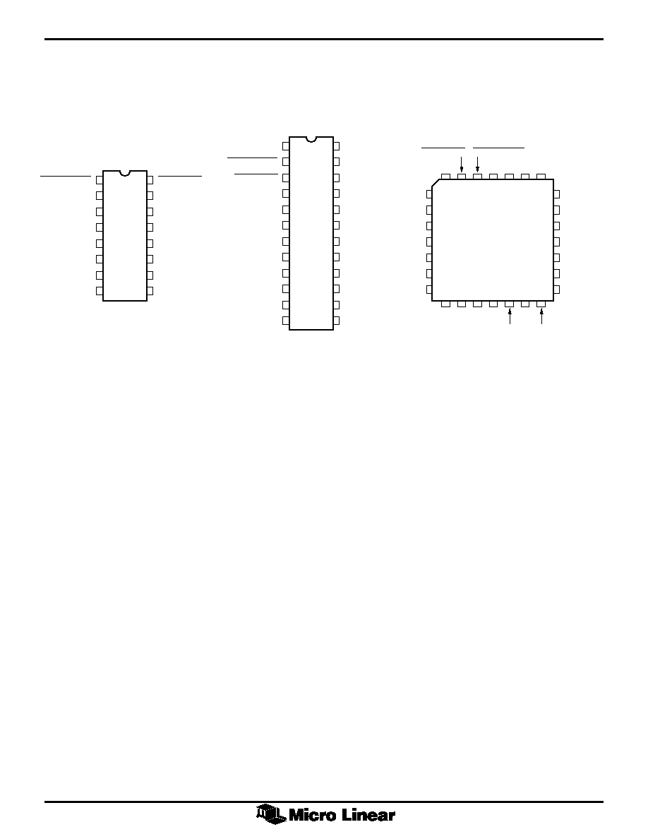
PIN CONNECTIONS
ML4624
24-Pin Narrow DIP
ML4624
28-Pin PCC
V
CC
NC
NC
C
TIMER
V
REF
V
TH
ADJ
GND
TTL OUT
V
CC
TTL
GND TTL
ECL+
ECL≠
NC
TTL LINK MON
CMP ENABLE
V
IN
≠
V
IN
+
V
DC
CF2
CF1
NC
NC
NC
NC
NC
C
TIMER
V
REF
V
TH
ADJ
GND
TTL OUT
V
CC
TTL
V
IN
≠
V
IN
+
NC
V
DC
CF2
CF1
NC
24
23
22
21
20
19
18
17
16
15
14
13
1
2
3
4
5
6
7
8
9
10
11
12
25
24
23
22
21
20
19
5
6
7
8
9
10
11
ML4622
16-Pin DIP or
SOIC (Narrow)
CMP ENABLE
V
TH
ADJ
V
REF
C
TIMER
V
CC
TTL OUT
ECL+
ECL≠
TTL LINK MON
GND
V
IN≠
V
IN
+
V
DC
CF2
CF1
GND TTL
16
15
14
13
12
11
10
9
1
2
3
4
5
6
7
8
TOP VIEW
TOP VIEW
NC NC NC NC ECL+
ECL≠ GND TTL
12 13 14 15 16 17 18
4 3 2 1 28 27 26
NC V
CC
NC NC
NC
TTL LINK MON
CMP ENABLE

3
ML4622, ML4624
PIN DESCRIPTION
NAME
FUNCTION
TTL LINK MON TTL Link Monitor output. Signal is
low when the V
IN
+, V
IN
≠ inputs
exceed the minimum threshold,
which is set by a voltage on the
V
TH
ADJ pin. Signal is high when the
input signal level is below the
threshold. Capable of driving a 10mA
LED indicator. This pin can be tied to
CMP ENABLE.
CMP ENABLE
A low voltage at this TTL input pin
enables both the ECL and the TTL
outputs. A high TTL voltage disables
the comparator output with ECL+
high, ECL≠ low, and TTL OUT high.
V
IN
≠
This input pin should be capacitively
coupled to the input source or to
filtered ground. (The input resistance
is approximately 1.6k
.)
V
IN
+
This input pin should be capacitively
coupled to the input source or to
filtered ground. (The input resistance
is approximately 1.6k
.)
ECL≠
The ECL comparator negative output.
Has internal pull down resistor.
External pull downs are not required
unless driving a large capacitive
load.
ECL+
The ECL comparator positive output.
Has internal pull down resistor.
External pull downs are not required
unless driving a large capacitive
load.
GND TTL
The negative supply for the TTL
comparator stage. If the TTL output is
not necessary, connect GND TTL
to V
CC
.
NAME
FUNCTION
V
CC
TTL
The positive supply for the TTL
comparator stage. If the TTL output is
not necessary, connect V
CC
TTL to
V
CC
. (ML4624 only)
TTL OUT
TTL data output.
V
DC
An external capacitor on this pin
integrates an error signal which nulls
the offset of the input amplifier. If the
DC feedback loop is not being used,
this pin should be connected to V
REF
.
CF2
A capacitor from this pin to CF1
controls the maximum bandwidth of
the amplifier.
CF1
Connect to CF2 through a capacitor.
GND
Negative supply. Connect to ≠5.2V
for ECL operation, or to ground for
TTL or raised ECL operation.
V
TH
ADJ
This input pin sets the link monitor
threshold.
V
REF
A 2.5V reference with respect to
GND.
C
TIMER
A capacitor from this pin to V
CC
determines the Link Monitor
response time.
V
CC
Positive supply. Connect to ground
for negative ECL operation, or to 5V
for TTL or raised ECL operation.

4
ML4622, ML4624
ABSOLUTE MAXIMUM RATINGS
V
CC
≠ GND . . . . . . . . . . . . . . . . . . . . . . . . . . . . . . ≠0.3 to +7.0
V
CC
TTL ≠ GND TTL . . . . . . . . . . . . . . . . . . . . . . . ≠0.3 to +7.0
Inputs/Outputs GND . . . . . . . . . . . . . . . . . . . ≠0.3 to V
CC
+0.3
Storage Temperature Range . . . . . . . . . . . . . . ≠65
∞
C to +150
∞
C
Lead Temperature (Soldering 10 sec.) . . . . . . . . . . . . . . +260
∞
C
ML4622, ML4624 ELECTRICAL CHARACTERISTICS (Note 2 and 3)
Over recommended operating conditions of T
A
= 0
∞
C to 70
∞
C for commercial temperature range, T
A
= ≠40
∞
C to +85
∞
C for
industrial temperature range, V
CC
= 5V
±
10%, GND = 0V unless otherwise noted (Note 1).
SYMBOL
PARAMETER
MIN
TYP
MAX
UNITS
CONDITIONS
I
CC1
V
CC
Supply Current
35
45
mA
GND TTL = V
CC
(TTL Output Disabled)
I
CC2
V
CC
Supply Current
55
70
mA
GND TTL = GND
(TTL Output Enabled)
V
REF
Reference Voltage
2.40
2.50
2.60
V
I
V
REF
V
REF
Output Source Current
5
mA
A
V
Amplifier Gain
100
V/V
V
IN
Input Signal Range
2
1600
mV
P≠P
V
TH
ADJ
External Voltage at V
TH
ADJ
0.5
2.6
V
Range
to set V
TH
V
OS
Input Offset
3
mV
V
DC
= V
REF
(DC loop inactive)
E
N
Input Referred Noise
25
µ
V
50MHz BW
BW
3dB Bandwidth
45
MHz
R
IN
Input Resistance
1
1.6
2.5
k
V
IN
+, V
IN
≠
I
V
TH
ADJ
Input Bias Current of V
TH
ADJ
≠200
10
+200
µ
A
t
PDTTL
Propagation Delay
15
ns
From V
IN
+, V
IN
≠ to TTL Out
V
IN
= 10mV
P≠P
t
PDECL
Propagation Delay
11
ns
From V
IN
+, V
IN
≠ to ECL+, ECL≠
V
IN
= 10mV
P≠P
TTL V
OH
2.4
V
V
CC
TTL = 5V, I
OH
= ≠50
µ
A
TTL V
OL
0.55
V
V
CC
TTL = 5V, I
OL
= 2mA
TTL V
IH
2.0
V
TTL V
IL
0.8
V
TTL I
IH
≠50
50
µ
A
V
IH
= 2.4V
TTL I
IL
≠1.6
0
mA
V
IH
= 0.4V

5
ML4622, ML4624
ML4622, ML4624 ELECTRICAL CHARACTERISTICS (Continued)
Over recommended operating conditions of T
A
= 0
∞
C to 70
∞
C for commercial temperature range, T
A
= ≠40
∞
C to +85
∞
C for
industrial temperature range, V
CC
= 5V
±
10%, GND = 0V unless otherwise noted.
SYMBOL
PARAMETER
MIN
TYP
MAX
UNITS
CONDITIONS
V
TH
Input Threshold Voltage
ML4622
4
5
6
mV
P≠P
V
TH
ADJ = V
REF
(note 4)
ML4624
5
6
7
mV
P≠P
V
TH
ADJ = V
REF
(note 4)
Hystersis
20
%
V
CM
Common mode voltage
1.65
V
on VIN+, VIN≠
ECL
V
OH
Output High Voltage at
V
CC
≠ 1.06
V
CC
≠ 0.7
With 200
load tied to
ECL+, ECL≠
V
CC
≠ 0.6
(note 5)
V
CC
≠ 2V
ECL
V
OL
Output Low Voltage at
V
CC
≠ 1.89
V
CC
≠ 1.62
With 200
load tied to
ECL+, ECL≠
V
CC
≠ 1.56
(note 5)
V
CC
≠ 2V
Note 1: Absolute maximum ratings are limits beyond which the life of the integrated circuit may be impaired. All voltages unless otherwise specified are measured with
respect to ground.
Note 2: Limits are guaranteed by 100% testing, sampling, or correlation with worst-case test conditions.
Note 3: Low Duty Cycle pulse testing is performed at T
A
.
Note 4: DC Tested -- Threshold for switching
TTL LINK MON from High (off) to Low (on).
Note 5: Industrial temperature range specification..