 | –≠–ª–µ–∫—Ç—Ä–æ–Ω–Ω—ã–π –∫–æ–º–ø–æ–Ω–µ–Ω—Ç: ML4642CR | –°–∫–∞—á–∞—Ç—å:  PDF PDF  ZIP ZIP |
April 1997
ML4642 AUI Multiplexer
GENERAL DESCRIPTION
The ML4642 AUI Multiplexer contains all the necessary
drivers/receivers and control logic to implement a 2 port
MAU when used in conjuction with a transceiver chip
which has a standard 802.3 AUI interface. In addition, the
ML4642 is capable of operating in stand-alone mode
where it interconnects two DTEs in the absence of a
network MAU. Several ML4642s can be cascaded
together to implement a 4 or 8 port MAU or stand-alone
device.
Logic within the ML4642 detects collisions resulting from
multiple DTEs transmitting simultaneously. In addition,
collision signals received from a transceiver attached at
the MAU port are propagated to both of the DTE ports.
Jabbering DTEs are prevented from loading down the
network by internal jabber timers which disable babbling
ports.
FEATURES
s
IEEE 802.3 compliant AUI interfaces assure
compatibility with any AUI ready devices
s
No crystal or clock input
s
On-chip Jabber logic, Collision Detection, and SQE
test with enable/disable option
s
Selectable Loopback, Jabber, and SQE Test allows
cascading of multiple chips to increase DTE port
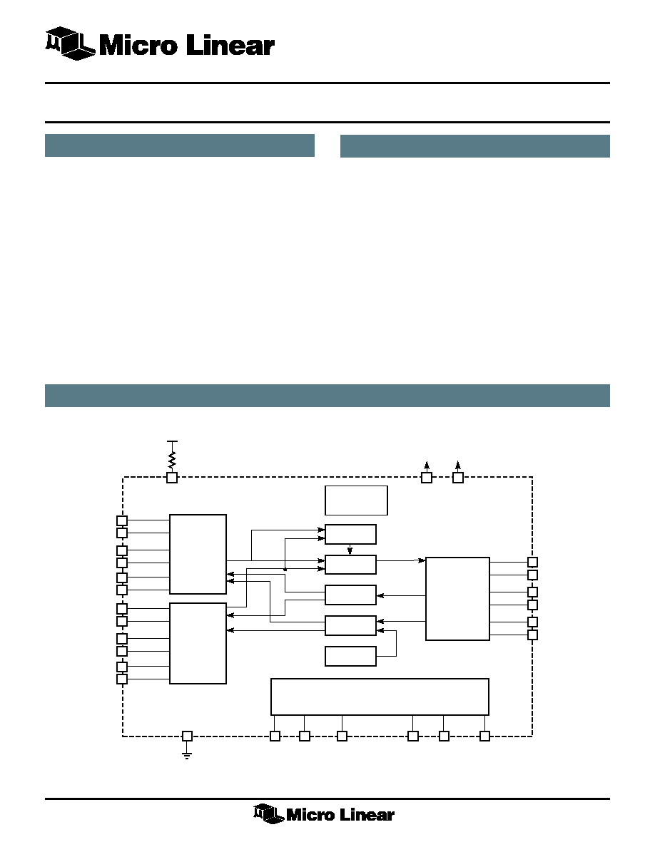
BLOCK DIAGRAM
1
V
CC
V
CC
GND
DTE
AUI
INTERFACE
MAU
AUI
INTERFACE
CONTROL
LOGIC
JABBER
DI MUX
CI MUX
SQE SOURCE
LED DRIVERS
+5V
61.9K
RRSET
TXOUTP
TXOUTN
RXINP
RXINN
CDINP
CDINN
JAB1/JDIS
JAB2
CDLED
RXLED/LPBK/SQE
TXLED1
TXLED2
MAU
AUI
INTERFACE
TXIN1P
TXIN1N
RXOUT1P
RXOUT1N
CDOUT1P
CDOUT1N
TXIN2P
TXIN2N
RXOUT2P
RXOUT2N
CDOUT2P
CDOUT2N
DO MUX

2
ML4642
PIN CONNECTIONS
TOP VIEW
RXLED/LPBK/SQE
RXINP
RXINN
JAB1/JDIS
RRSET
V
CC
TXOUTP
TXOUTN
TXLED1
TXLED2
TXIN2P
TXIN2N
TXIN1P
TXIN1N
RXOUT1P
RXOUT1N
RXOUT2N
RXOUT2P
GND
CDOUT1N
CDOUT1P
JAB2
CDINP
CDINN
CDLED
CDOUT2P
CDOUT2N
V
CC
1
2
3
4
5
6
7
8
9
10
11
12
13
14
28
27
26
25
24
23
22
21
20
19
18
17
16
15
ML4642
28-Pin SSOP (R28)
ML4642
28-Pin PLCC (Q28)
RXOUT2P
GND
CDOUT1N
CDOUT1P
JAB2
CDINP
CDINN
RRSET
V
CC
TXOUTP
TXOUTN
TXLED1
TXLED2
TXIN2P
12
13 14
15
16
JAB1/JDIS
RXINN
RXINP
RXLED/LPBK/SQE
RXOUT1P
RXOUT1N
RXOUT2N
TXIN2N
TXIN1P
TXIN1N
V
CC
CDOUT2N
CDOUT2P
CDLED
17
18
5
6
7
8
9
10
11
4
3
2
1
28
25
24
23
22
21
20
19
27
26
TOP VIEW
3
ML4642
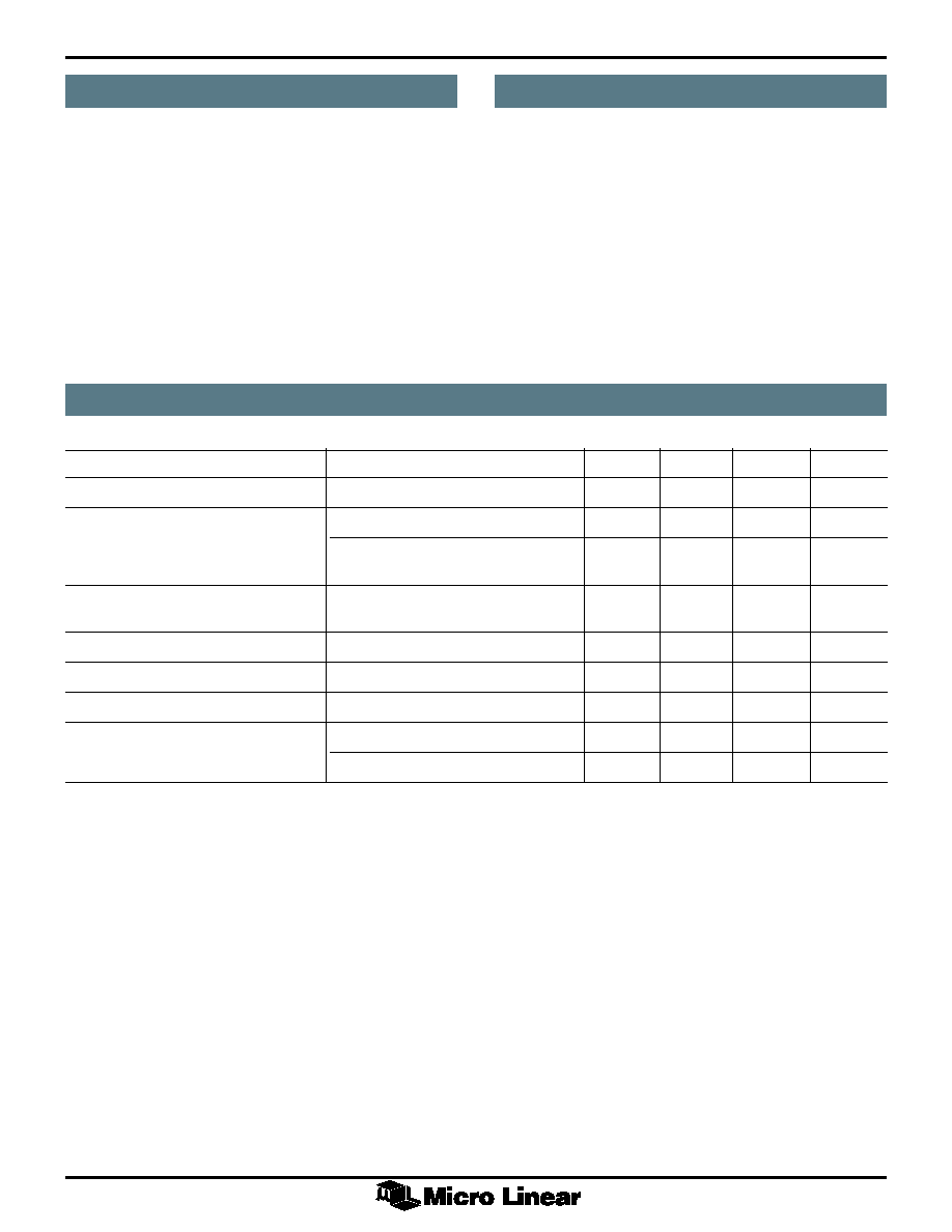
PIN DESCRIPTIONS
PIN NO.
NAME
FUNCTION
DESCRIPTION
1
RXLED/LPBK/SQE
I/O
Active low receive LED driver for MAU port. If tied to ground, this pin
enables internal loopback of the active TXIN pair to the RXOUT pairs
and enables SQE test. If tied to 0.6 volts internal loopback is enable but
SQE test is disabled. SQE and loopback are disabled when this pin is
pulled high.
2
RXINP
Input
Receive signal pair for MAU port.
3
RXINN
Onput
Receive signal pair for MAU port.
4
JAB1/JDIS
I/O
Active low jabber LED driver for DTE port 1. If tied to ground, the
jabber function is disabled at TXIN1 and TXIN2.
5
RRSET
Input
Bias setting external resistor, 61.9K˝.
6
V
CC
Power
+5 volt power supply
7
TXOUTP
Output
Transmit signal pair for MAU port.
8
TXOUTN
Output
Transmit signal pair for MAU port.
9
TXLED1
Output
Open collector, active low transmit LED driver for DTE AUI port 1.
10
TXLED2
Output
Open collector, active low transmit LED driver for DTE AUI port 2.
11
TXIN2P
Input
Transmit signal pair for DTE port 2.
12
TXIN2N
Input
Transmit signal pair for DTE port 2.
13
TXIN1P
Input
Transmit signal pair for DTE port 1.
14
TXIN1N
Input
Transmit signal pair for DTE port 1.
15
V
CC
Power
+5 volt power supply
16
CDOUT2N
Output
Collision signal pair for DTE port 2.
17
CDOUT2P
Output
Collision signal pair for DTE port 2.
18
CDLED
Output
Open collector, active low collision LED driver.
19
CDINN
Input
Collision signal pair for MAU port.
20
CDINP
Input
Collision signal pair for MAU port.
21
JAB2
Output
Open collector, active low jabber LED driver for DTE port 2.
22
CDOUT1P
Output
Collision signal pair for DTE port 1.
23
CDOUT1N
Output
Collision signal pair for DTE port 1.
24
GND
Ground
GND.
25
RXOUT2P
Output
Receive signal pair for DTE port 2.
26
RXOUT2N
Output
Receive signal pair for DTE port 2.
27
RXOUT1N
Output
Receive signal pair for DTE port 1.
28
RXOUT1P
Output
Receive signal pair for DTE port 1.
4
ML4642
ABSOLUTE MAXIMUM RATINGS
Absolute maximum ratings are limits beyond which the
life of the integrated circuit may be impaired. All
voltages unless otherwise specified are measured with
respect to ground.
Power Supply Voltage Range V
CC
. . . GND ≠0.3V to 6.0V
Input Current RRSET, JAB1/JABD, JAB2, CDLED,
RxLED/LPBK/SQE, TxLED1, TxLED2 . . . . . . . . . . 60mA
Junction Temperature . . . . . . . . . . . . . . . . . . . . . . 150∞C
Storage Temperature . . . . . . . . . . . . . . . . ≠65∞C to 150∞C
Lead Temperature (Soldering 10 seconds) . . . . . . . 260∞C
Thermal Resistance (
q
JA
)
SSOP . . . . . . . . . . . . . . . . . . . . . . . . . . . . . . 109∞C/W
PLCC . . . . . . . . . . . . . . . . . . . . . . . . . . . . . . . 68∞C/W
OPERATING CONDITIONS
Supply Voltage (V
CC
) . . . . . . . . . . . . . . . . . . . 5V ± 10%
LED on Current . . . . . . . . . . . . . . . . . . . . . . . . . . . . 10mA
RRSET . . . . . . . . . . . . . . . . . . . . . . . . . . . . 61.9k˝ ± 1%
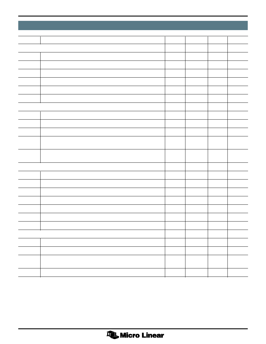
ELECTRICAL CHARACTERISTICS
Unless otherwise specified T
A
= 0∞C to 70∞C, V
CC
= 5V ± 10%. (Notes 1, 2)
PARAMETER
CONDITIONS
MIN
TYP.
MAX
UNITS
Power Supply Current I
CC
V
CC
= 5V, (Note 3)
60
120
mA
LED Drivers: V
OL
R
L
=510˝ for CDLED, TXLED1,2, JAB2
0.8
V
R
L
=270˝ for JAB1/JDIS,
RxLED/LPBK/SQE
1.2
2.5
3.5
V
Transmit Squelch Voltage Level
≠300
≠250
≠200
mV
(Tx+, Tx≠)
Differential Output Voltage
±550
±1200
mV
Common Mode Output Voltage
4.0
V
Differential Output Voltage Imbalance
2
±40
mV
RxLED/LPBK/SQE
SQE Enabled/Loopback Enabled
0.3
V
SQE Disabled/Loopback Enabled
0.4
0.6
0.8
V
Note 1: Limits are guaranteed by 100% testing, sampling or correlation with worst case test conditions.
Note 2: Low Duty cycle pulse testing is performed at T
A
.
Note 3: This does not include the current from the AUI pull down resistors or the LED output pins.
5
ML4642
AC ELECTRICAL CHARACTERISTICS
SYMBOLS
PARAMETER
MIN
TYP.
MAX
UNITS
TRANSMIT
t
TXNPW
Transmit Turn-On Pulse Width
20
ns
t
TXFPW
Transmit Turn-Off Pulse Width
180
ns
t
XODY
Transmitter Turn-On Delay
30
ns
t
TXLP
Transmit Loopback Startup Delay
40
ns
t
TXSDY
Transmit Steady State Prop. Delay
15
ns
t
TXJ
Transmitter Jitter
1
ns
RECEIVE
t
RXODY
Receive Turn-On Delay
20
ns
t
RXSDY
Receive Steady State Prop. Delay
15
ns
t
RXJ
Receiver Jitter
1
ns
t
AR
Differential Output Rise Time
3
ns
20% to 80% (Rx+/≠, COL+/≠)
t
AF
Differential Output Fall Time
3
ns
20% to 80% (Rx+/≠, COL+/≠)
COLLISION
t
CPSQE
Collision Present to SQE Assert
0
200
ns
t
SQEXR
Time for SQE to Deactivate after a collision
100
900
ns
t
CLF
Collision Frequency
8.5
10
11.5
MHz
t
CLPDC
Collision Pulse Duty Cycle
40
50
60
%
t
SQEDY
SQE Test Delay (Tx Inactive to SQE)
0.6
1.1
1.6
µs
t
SQETD
SQE Test Duration
0.5
1.0
1.5
µs
t
SQEB
SQE Blank Period
4
7
µsec
JABBER, LINK TEST AND LED TIMING
t
JAD
Jabber Activation Delay
7
13.5
20
ms
t
JRT
Jabber Reset Unjab Time
250
450
750
ms
t
JSQE
Delay from Outputs Disabled to
100
ns
Collision Oscillator On
t
LEDT
CDLED, RxLED, TxLED1, TxLED2 On Time
20
50
300
ms

6
ML4642
Figure 2. Receive Timing
TIMING DIAGRAMS
t
TXNPW
VALID
DATA
t
TXODY
DATA
VALID
t
TXFPW
t
TXSDY
t
TXLP
TXINP
TXINN
TXOUTP
TXOUTN
RXOUT1, 2, P
RXOUT1, 2, N
VALID
DATA
VALID
DATA
t
RXODY
t
RXSDY
DATA
VALID
t
AF
t
AR
RXINP
RXINN
RXOUT1, 2, P
RXOUT1, 2, N
Figure 1. Transmit and Loopback Timing
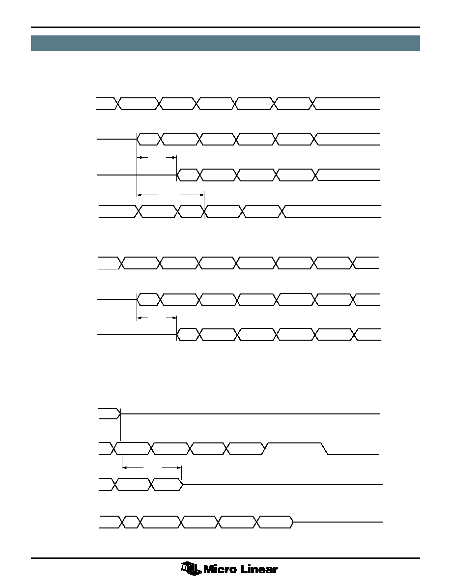
7
ML4642
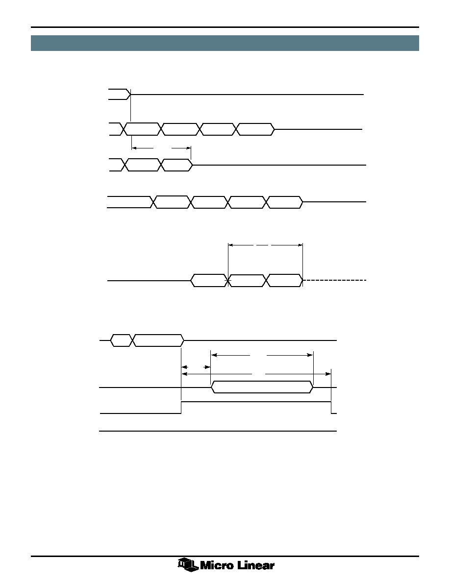
TIMING DIAGRAMS (Continued)
Figure 4. Collision Timing
Figure 3. Collision Timing
VALID
DATA
VALID
DATA
CS0
t
CPSQE
VALID
DATA
VALID
DATA
t
CPSQE
CS0
TXIN2P
TXIN2N
TXIN1P
TXIN1N
CDOUT1, 2, P
CDOUT1, 2, N
TXOUTP
TXOUTN
TXIN1P
TXIN1N
TXIN2P
TXIN2N
CDOUT1, 2, P
CDOUT1, 2, N
t
TX2, TX1
TXIN2
TXIN2
TXIN2
TXIN1
TXIN1
TXIN1
VALID
DATA
t
SQEXR
CS0
TXIN1P
TXIN1N
TXIN2P
TXIN2N
CDOUT1, 2, P
CDOUT1, 2, N
TXOUTP
TXOUTN
TXIN1
TXIN1
TXIN2
TXIN2
TXIN2
TXIN2
8
ML4642
t
SQETD
TXIN1N
VALID DATA
t
SQEDY
t
SQEB
CS0
TXIN1P
CDOUT1P
t
SQEB
CDOUT2P
CDOUT2N
CDOUT1N
(internal signal)
TIMING DIAGRAMS (Continued)
Figure 5. Collision Timing
Figure 6. SQE Timing
VALID
DATA
t
SQEXT
CS0
TXIN2P
TXIN2N
TXIN1P
TXIN1N
CDOUT1, 2, P
CDOUT1, 2, N
TXOUTP
TXOUTN
TXIN1
TXIN1
TXIN1
TXIN1
TXIN1
CDOUT1, 2, P
CDOUT1, 2, N
1
t
CLF
9
ML4642
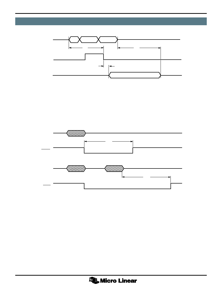
Figure 8. LED Timing
TIMING DIAGRAMS (Continued)
Figure 7. Jabber Timing
CS0
TXIN1P
TXIN1N
CDOUT1P
CDOUT1N
VALID
DATA
VALID
DATA
t
JSQE
t
JAD
t
JRT
TXOUTP
TXOUTN
TXOUT1P
TXOUT1N
RXINP
RXINN
t
LEDT
TXLED1
t
LEDT
RXLED
10
ML4642
39
39
360
360
360
360
39
39
360
360
360
360
39
39
39
39
360
360
TXIN1P
TXIN1N
RXOUT1P
RXOUT1N
CDOUT1P
CDOUT1N
TXIN2P
TXIN2N
RXOUT2P
RXOUT2N
CDOUT2P
CDOUT2N
TXOUTP
TXOUTN
RXINP
RXINN
CDINP
CDINN
JAB1/JABD
JAB2
CDLED
TXLED1
TXLED2
RXLED/LPBK/SQE
V
CC
V
CC
GND
Switch Option
1. Receive LED with Internal/External MAU
2. No MAU/No SQE
3. No MAU with SQE
ML4642
0.1
0.01
+5V
61.9K
+5V
RRSET
510
510
510
510
270
270
2
+5V
3
TO MAU
TO DTE 1
TO DTE 2
1
Q1
1k
1k
7.15k
Q2
Before data will be transmitted to the TXOUT and RXOUT
pins from the TXIN pins it must meet the unsquelch
requirements of the TXIN receiver circuitry. The squelch
circuitry prevents any noise on the TXIN wires from being
misinterpreted as data and transmitted to the TXOUT and
RXOUT pins. The squelch circuit rejects signals with pulse
widths less than typically 20ns and voltage levels more
positive than ≠250mV. Once the TXIN receiver is
unsquelched it remains so until reception of the input idle
signal, which is detected when the TXIN signal is more
positive than ≠170mV for longer than 180ns.
RECEPTION
The receive function consists of detecting data at the
RXIN differential receiver of the MAU port transmitting
this data to both DTE port RXOUT pairs.
Figure 9 is a block diagram of a Two Port Multiplexer
using the ML4642 chip. All AUI interfaces are shown AC
coupled as they would be in an AUI multiplexer which
does not include the MAU circuitry on the same board.
TRANSMISSION
The transmit function consists of detecting data on either
of the TXIN differential receivers (TXIN1 or TXIN2) and
transmitting this data out the TXOUT differential driver at
the MAU port as well as both RXOUT1 and RXOUT2
drivers of the DTE ports. (Note: the looping back of data
received at a TXIN pair to the RXOUT pairs is discussed in
the Loopback section.)
Figure 9. Two Port AUI Multiplexer
FUNCTIONAL DESCRIPTION

11
ML4642
Before data will be transmitted to the RXOUT pins of the
DTE ports it must meet the unsquelch requirements for the
RXIN receiver circuitry. The squelch circuitry at the RXIN
differential receiver input performs the same function as
that of the TXIN squelch circuitry using the same noise
rejection criteria.
COLLISION
There are two conditions that constitute a collision from
the point of view of the ML4642:
a) If data is received at the TXIN inputs of both DTE ports
simultaneously a local collision occurs within the
ML4642.
b) If the CDIN input is active at any time other than the
inter-packet gap window allowed for the SQE Test
function described below.
In either of the above circumstances it is necessary for the
ML4642 to drive the CDOUT pairs on both DTE ports with
the collision signal. The collision signal consists of a 10
MHz +/≠ 15% square wave matching the AUI
specifications and capable of driving a 78˝ load. The
collision signal shall turn on within 2 bit times of the
origination of the collision condition and shall turn off
within 2≠5 bit times after the collision condition subsides.
During a collision condition there are two sources for data
to be transmitted to TXOUT, TXIN1 and TXIN2. The highest
priority source for data to be transmitted to TXOUT is the
TXIN1 receiver.
For example if TXIN2 begins transmission then TXIN1 turns
on, the collision oscillator will turn on and TXOUT will
switch from TXIN2 to TXIN1. If the collision ends by
TXIN1 turning off first, TXOUT will switch from TXIN1 to
TXIN2, and 2≠5 bit times later the collision oscillator will
turn off.
The MAU port's CDIN receiver contains squelch circuitry
to prevent noise from causing the erroneous detection of a
collision signal. A signal on the CDIN pair will not be
considered active until it exceeds the same squelch
requirements as those of the TXIN receivers.
LOOPBACK
The loopback function allows the ML4642 to emulate a
coaxial transceiver by propagating the TXIN data back
out the RXOUT pair of the same DTE port that is sourcing
the data as well as the RXOUT pair of the idle DTE port.
This allows the Ethernet controller sending the data to
monitor its transmit packets and detect network faults.
The loopback function is enabled at both DTE ports when
the RXLED pin is tied to ground, or 0.6 volts.
SQE TEST FUNCTION
The Signal Quality Error (SQE) Test function allows the
DTE to determine whether or not the collision detection
circuitry is functional. After each transmission, during the
inter-packet gap time, the collision signal will be
activated on the CDOUT pair of the same port as the
TXIN pair which received the packet, for typically 1 µs.
The SQE function will not be activated on DTE ports of
the ML4642 which are in the Jabber state. The SQE
function is enabled on both DTE ports when the RXLED/
LPBK/SQE pin is grounded.
JABBER
The jabber function prevents a babbling transmitter from
loading down the network. Within the ML4642 is a jabber
timer on each TXIN receiver. Each timer starts at the
beginning of a received packet and resets at the end of
each packet. If a packet lasts longer than 7 to 20ms the
jabber logic disables its corresponding TXIN receiver (thus
preventing its data from being retransmitted) and
generates a collision signal on the babbling port's CDOUT
pair. When the TXIN pair finally goes idle, a second timer
measures 0.5 seconds of idle on TXIN prior to re-enabling
the receiver and turning off the collision signal. If the
TXIN pair becomes active again before the 0.5 seconds
has expired, the timer is reset and measures another 0.5
seconds of idle time.
The jabber function can be disabled on both ports by tying
the JAB1/JABD pin to ground.
LED DRIVERS
The ML4642 has six LED driver pins. Each DTE port has a
transmit LED and a jabber LED and the MAU port has a
receive LED. Additionally, there is a collision LED which
indicates the presence of a collision condition. All LED
drivers are active low 10mA current sources.
The TXLED, RXLED, and CDLED outputs have 50ms pulse
stretchers on them to enable the LEDs to be visible. The
JLED outputs do not have pulse stretchers on them
because their conditions occur long enough for the LEDs
to be visible.
Two of the ML4642 LED outputs serve as configuration
pins as well. RXLED/LPBK/SQE and JAB1/JDIS may be
tied through a resistor to V
CC
, tied through a resistor and a
LED to V
CC
or grounded. Additionally RXLED/LPBK/SQE
may be tied to a specific voltage. When these pins are
grounded or tied to a 0.6 Volts they become configuration
inputs. Otherwise when tied high they become status
outputs.
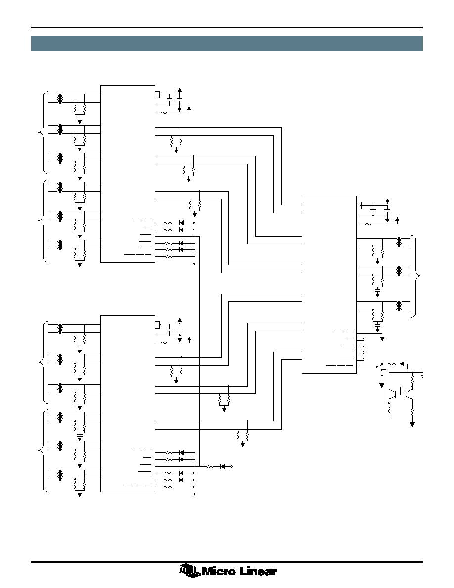
CASCADING THE ML4642 FOR 4 AND 8 PORT DESIGNS
The configurability of such functions as loopback, jabber,
and SQE allows ease of cascading multiple ML4642 chips
for larger fan-out designs. Figure 10 shows a four port AUI
Multiplexer design. For a type 0 configuration both jabber
and transmit LEDs are available on a per port basis for
status. The RXLED/LPBK/SQE pins are tied through a
resistor to 5 volts, and CDLED is wire OR'ED with the
other chip for one collision detect status LED per system.
There is also only one receive LED status output which is
displayed in a type 2 configuration. This particular pin in
FUNCTIONAL DESCRIPTION
12
ML4642
Figure 10. Four Port AUI Multiplexer
39
39
360
360
360
360
39
39
360
360
360
360
TXIN1P
TXIN1N
RXOUT1P
RXOUT1N
CDOUT1P
CDOUT1N
TXIN2P
TXIN2N
RXOUT2P
RXOUT2N
CDOUT2P
CDOUT2N
TXOUTP
TXOUTN
RXINP
RXINN
CDINP
CDINN
JAB1/JABD
JAB2
CDLED
TXLED1
TXLED2
RXLED/LPBK/SQE
V
CC
V
CC
GND
ML4642
RSSET
TO DTE 1
TO DTE 2
39
39
360
360
360
360
39
39
360
360
360
360
TXIN1P
TXIN1N
RXOUT1P
RXOUT1N
CDOUT1P
CDOUT1N
TXIN2P
TXIN2N
RXOUT2P
RXOUT2N
CDOUT2P
CDOUT2N
TXOUTP
TXOUTN
RXINP
RXINN
CDINP
CDINN
JAB1/JABD
JAB2
CDLED
TXLED1
TXLED2
RXLED/LPBK/SQE
V
CC
V
CC
GND
Switch Options
1. Receive LED with Internal/External MAU
2. No MAU/No SQE
3. No MAU with SQE
ML4642
RSSET
TO DTE 3
TO DTE 4
0.1
0.01
+5V
+5V
39
39
39
39
360
360
TXIN1P
TXIN1N
RXOUT1P
RXOUT1N
CDOUT1P
CDOUT1N
TXIN2P
TXIN2N
RXOUT2P
RXOUT2N
CDOUT2P
CDOUT2N
TXOUTP
TXOUTN
RXINP
RXINN
CDINP
CDINN
JAB1/JABD
JAB2
CDLED
TXLED1
TXLED2
RXLED/LPBK/SQE
V
CC
V
CC
GND
ML4642
0.1
0.01
+5V
+5V
RSSET
NC
TO MAU
0.1
0.01
+5V
+5V
1K
1K
1K
1K
510
510
510
270
+5V
270
510
+5V
1k
1k
1k
1k
1k
1k
510
510
510
270
+5V
270
1k
1k
NC
NC
NC
61.9k
61.9K
61.9k
Type 0
Type 2
270
2
+5V
3
1
Q1
1k
1k
Q2
7.15k
FUNCTIONAL DESCRIPTION
13
ML4642
SQE TEST WHEN CASCADING
As mentioned before, after each transmission during the
interpacket gap time the collision signal will be activated
on the CDOUT pair of the same port as the TXIN pair
which received the packet. When cascading ML4642s to
implement 4 or 8 port designs, the path is remembered
and followed to acheive this function. The paths that did
not carry the transmit data blocks CDOUT for 4-7 µsec
after transmission to guarantee that only the port that
transmitted will see SQE test.
a type 2 configuration offers three options. In option 1,
when tied to +5 volts through a resistor and an LED, an
internal or external MAU will be connected. For stand-
alone operation without an internal or external MAU a
loopback is required. Option 2 allows loopback with no
SQE test while option 3 provides loopback with an SQE
test.
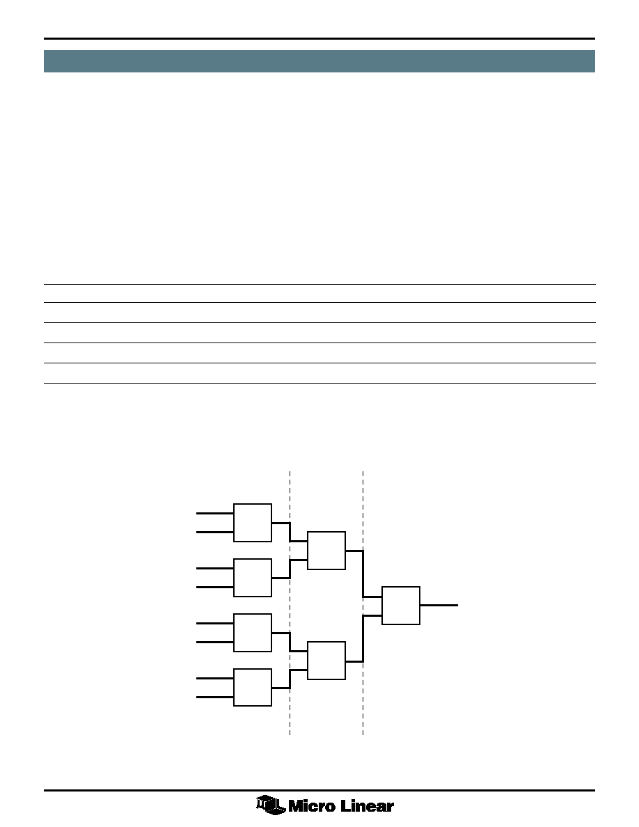
An eight port design is accomplished in the same way as
shown in the block diagram in Figure 11. In an eight port
design Type 0 and Type 2 configuration remain the same
as in a four port design. Type 1 however only differs from
Type 2 by tying RXLED/LPBK/SQE through a resistor to +5
volts. Table 1 summerizes all of the different LED
configurations.
TABLE 1. LED Configurations for 2, 4, and 8 Port Designs
JAB1/JABD
RXLED/LPBK/SQE
JAB2
CDLED
TXLED1
TXLED2
Two Port AUI Mux
LED
GND, 0.6V, LED
LED
LED
LED
LED
Type 0
LED
270˝ to +5V
LED
WIRE'ORED
LED
LED
Type 1
GND
270˝ to +5V
NC
NC
NC
NC
Type 2
GND
GND, 0.6V, LED
NC
NC
NC
NC
DTE PORT 1
DTE PORT 2
DTE PORT 3
DTE PORT 4
DTE PORT 5
DTE PORT 6
DTE PORT 7
DTE PORT 8
ML4642
ML4642
ML4642
ML4642
ML4642
ML4642
ML4642
MAU PORT
TYPE 0
TYPE 1
TYPE 2
Figure 11. Eight Port AUI Multiplexer
FUNCTIONAL DESCRIPTION
14
ML4642
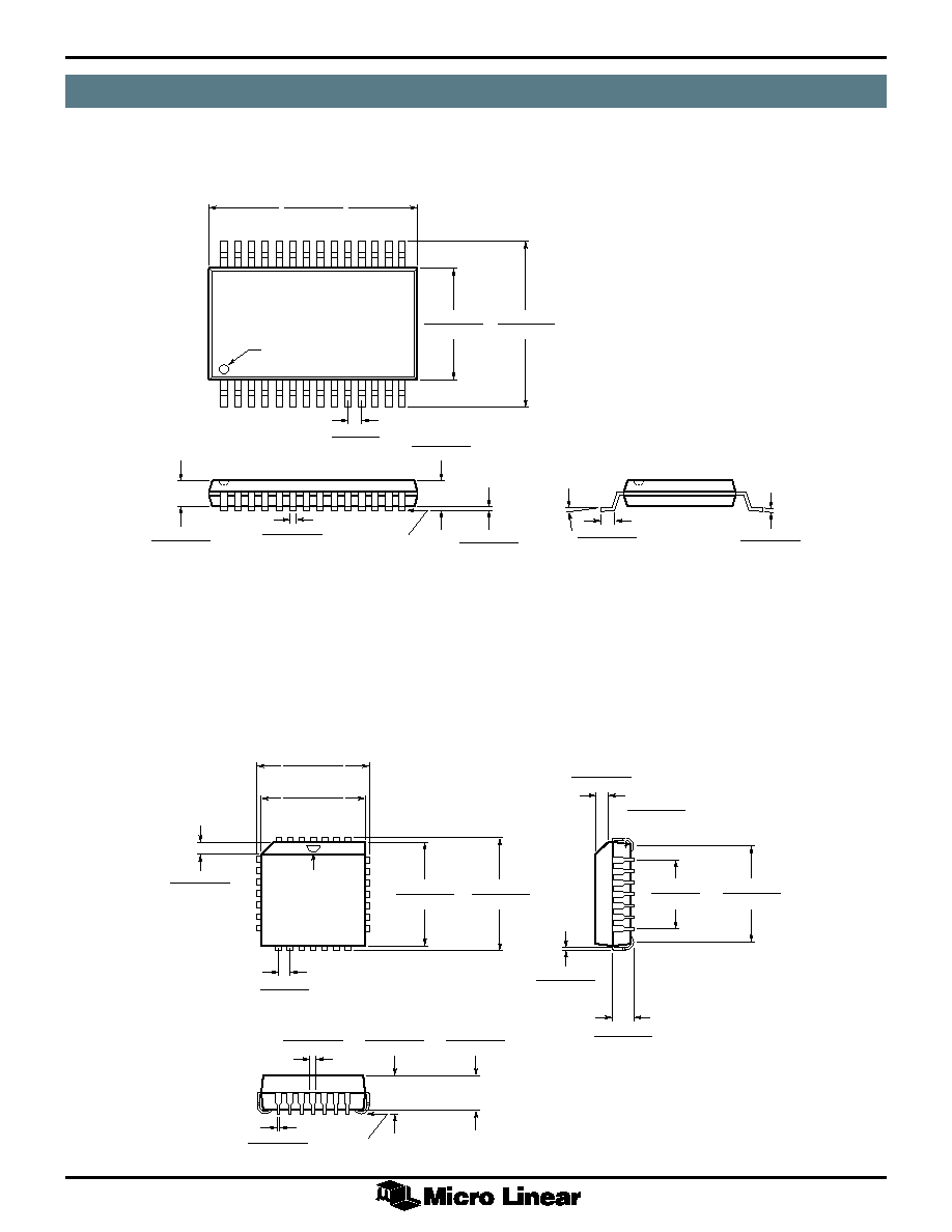
PHYSICAL DIMENSIONS inches (millimeters)
SEATING PLANE
0.205 - 0.213
(5.20 - 5.40)
0.301 - 0.313
(7.65 - 7.95)
0.397 - 0.407
(10.08 - 10.34)
0.009 - 0.015
(0.23 - 0.38)
0.026 BSC
(0.65 BSC)
0.022 - 0.030
(0.55 - 0.95)
0.068 - 0.078
(1.73 - 1.98)
0.002 - 0.008
(0.05 - 0.20)
0.066 - 0.070
(1.68 - 1.78)
0.004 - 0.008
(0.10 - 0.20)
0∫ - 8∫
PIN 1 ID
28
1
Package: R28
28-Pin SSOP
0.099 - 0.110
(2.51 - 2.79)
PIN 1 ID
SEATING PLANE
0.485 - 0.495
(12.32 - 12.57)
0.450 - 0.456
(11.43 - 11.58)
0.013 - 0.021
(0.33 - 0.53)
0.165 - 0.180
(4.06 - 4.57)
1
0.450 - 0.456
(11.43 - 11.58)
0.485 - 0.495
(12.32 - 12.57)
8
15
22
0.025 - 0.045
(0.63 - 1.14)
(RADIUS)
0.050 BSC
(1.27 BSC)
0.009 - 0.011
(0.23 - 0.28)
0.026 - 0.032
(0.66 - 0.81)
0.042 - 0.048
(1.07 - 1.22)
0.148 - 0.156
(3.76 - 3.96)
0.042 - 0.056
(1.07 - 1.42)
0.390 - 0.430
(9.90 - 10.92)
0.300 BSC
(7.62 BSC)
Package: Q28
28-Pin PLCC

15
ML4642
Micro Linear reserves the right to make changes to any product herein to improve reliability, function or
design. Micro Linear does not assume any liability arising out of the application or use of any product
described herein, neither does it convey any license under its patent right nor the rights of others. The
circuits contained in this data sheet are offered as possible applications only. Micro Linear makes no
warranties or representations as to whether the illustrated circuits infringe any intellectual property rights of
others, and will accept no responsibility or liability for use of any application herein. The customer is urged
to consult with appropriate legal counsel before deciding on a particular application.
2092 Concourse Drive
San Jose, CA 95131
Tel: 408/433-5200
Fax: 408/432-0295
ORDERING INFORMATION
PART NUMBER
TEMPERATURE RANGE
PACKAGE
ML4642CR
0∞C to 70∞C
28-Pin SSOP (R28)
ML4642CQ
0∞C to 70∞C
28-Pin PLCC (Q28)
© Micro Linear 1997
is a registered trademark of Micro Linear Corporation
Products described in this document may be covered by one or more of the following patents, U.S.: 4,897,611; 4,964,026; 5,027,116; 5,281,862; 5,283,483; 5,418,502; 5,508,570; 5,510,727; 5,523,940; 5,546,017;
5,559,470; 5,565,761; 5,592,128; 5,594,376; Japan: 2598946; 2619299. Other patents are pending.
DS4642-01