 | –≠–ª–µ–∫—Ç—Ä–æ–Ω–Ω—ã–π –∫–æ–º–ø–æ–Ω–µ–Ω—Ç: ML4668 | –°–∫–∞—á–∞—Ç—å:  PDF PDF  ZIP ZIP |
March 1997
ML4668
Low Power Single Chip 10BASE-FL Transceiver
GENERAL DESCRIPTION
The ML4668 single-chip 10BASE-FL transceiver is a low
power, high output current, plug-compatible version of the
industry standard ML4663. The ML4668 offers a standard
IEEE 802.3 AU interface that allows it to be directly
connected to industry standard manchester encoder/
decoder chips or an AUI connector.
The ML4668 provides a highly integrated solution that
requires a minimal number of external components, and is
compliant to the IEEE 802.3 10BASE-FL standard. The
transmitter offers a 100mA maximum current drive output
that directly drives a fiber optic LED transmitter. The
receiver offers a highly stable fiber optic data quantizer
capable of accepting input signals as low as 2mV
P-P
with a
55dB dynamic range.
The transmitter automatically inserts 1MHz signal during
idle time and removes this signal on reception. Low Light is
continuously monitored for both activity as well as power
level. Five LED status indicators monitor error conditions as
well as transmissions, receptions and collisions.
FEATURES
s
Single chip solution for 10BASE-FL internal or external
Medium Attachment Units (MAUs)
s
Incorporates an AU interface
s
Highly stable data quantizer with 55dB input
dynamic range
s
Input sensitivity as low as 2mV
P-P
s
Up to 100mA maximum current driven fiber optic LED
driver for accurate launch power
s
Single +5 volt supply
s
No crystal or clock required
s
Five network status LED outputs
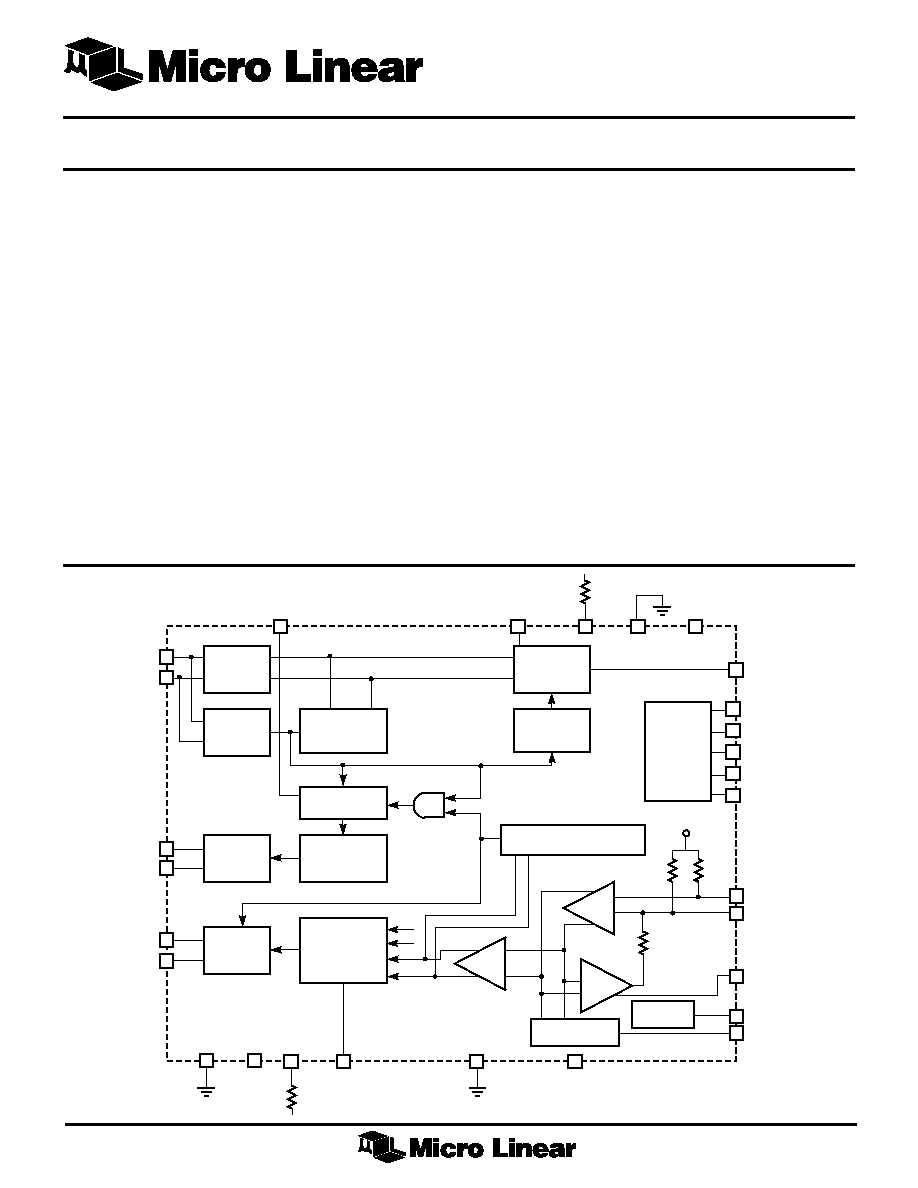
BLOCK DIAGRAM
1
AUI
RECEIVER
Tx
SQUELCH
AUI
DRIVER
AUI
DRIVER
10MHz GATED
OSCILLATOR
LOOPBACK
MUX
JABBER
RECEIVE SQUELCH
LINK DETECT
V
REF
LED
DRIVERS
FIBER OPTIC
LED
DRIVER
1MHz IDLE
SIGNAL
SQE
GND
V
CC
(+5V)
+5V
LBDIS
AGND
C
TIMER
RRSET
Tx
Rx
BIAS
GND
V
CC
Tx
(+5V)
+5V
RTSET
SQEN/JABD
Tx+
Tx≠
COL+
COL≠
Rx+
Rx≠
AV
CC
TxOUT
V
IN
+
V
DC
V
REF
V
THADJ
V
IN
≠
CMP
AMP
LMON
14
JAB
28
CLSN
1
RCV
16
XMT
15
18
27
20
12
17
5
10
11
2
3
6
7
19
9
13
8
24
4
23
22
21
25
26
2
ML4668
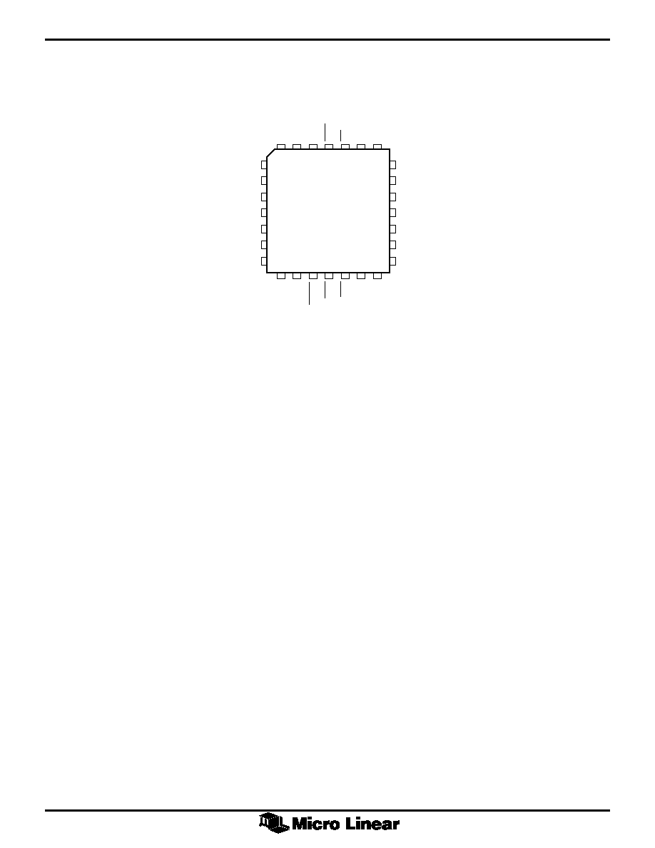
PIN CONNECTION
V
IN
≠
AGND
V
THADJ
V
REF
V
DC
GND
GND
SQEN/JABD
Rx+
Rx≠
LBDIS
V
CC
Tx+
Tx≠
25
24
23
22
21
20
19
5
6
7
8
9
10
11
12 13 14 15 16 17 18
4 3 2 1 28 27 26
RTSET
RRSET
LMON
XMT
RCV
V
CC
Tx
TxOUT
C
TIMER
COL≠
COL+
CLSN
JAB
AV
CC
V
IN
+
ML4668
28-Pin PLCC (Q28)

3
ML4668
PIN
NAME
FUNCTION
15
XMT
Indicates that transmission is taking
place. Active low LED driver, open
collector. Event is extended with
internal timer for visibility.
16
RCV
Indicates that the transceiver is
receiving a frame from the optical
input. Active low LED driver, open
collector. Event is extended with
internal timer for visibility.
17
V
CC
Tx
+5 volt supply for fiber optic LED
driver.
18
TxOUT
Fiber optic LED driver output.
19
GND
Ground Reference.
20
GND
Ground Reference.
21
V
DC
An external capacitor on this pin
integrates an error signal which
nulls the offset of the input
amplifier. If the DC feedback loop is
not being used, this pin should be
connected to V
REF
.
22
V
REF
A 2.5V reference with respect to
GND.
23
V
THADJ
This input pin sets the link monitor
threshold.
24
AGND
Analog Filtered Ground.
25
V
IN
≠
This input pin should be
capacitively coupled to the input
source or to filtered AV
CC
. (The
input resistance is approximately
1.3k
.)
26
V
IN
+
This input pin should be
capacitively coupled to the input
source or to filtered AV
CC
. (The
input resistance is approximately
1.3k
.)
27
AV
CC
Analog Filtered +5 volts.
28
JAB
Jabber network status LED. When in
the Jabber state, this pin will be low
and the transmitter will be disabled.
In the Jabber "OK" state this pin will
be high. Active low LED, open
collector.
PIN DESCRIPTION
PIN
NAME
FUNCTION
1
CLSN
Indicates that a collision is taking
place. Active low LED driver, open
collector. Event is extended with
internal timer for visibility.
2
COL+
Gated 10MHz oscillation used to
3
COL≠
indicate a collision, SQE test, or
jabber. Balanced differential line
driver outputs that meet AUI
specifications.
4
C
TIMER
A capacitor from this pin to V
CC
determines the Link Monitor
response time.
5
SQEN/JABD SQE Test Enable, Jabber Disable.
When tied low, SQE test is disabled,
when tied high SQE test is enabled.
When tied to 2.0V both SQE test and
Jabber are disabled.
6
Rx+
Manchester encoded receive data
7
Rx≠
output to the local device. Balanced
differential line driver outputs that
meet AUI specifications.
8
LBDIS
Loopback Disable. When this pin is
tied to V
CC
, the AUI transmit pair
data is not looped back to the AUI
receive pair, and collision is disabled.
When this pin is tied to GND
(normal operation) or left floating, the
AUI transmit pair data is looped back
to the AUI receiver pair, except
during collision.
9
V
CC
+5 volt power input.
10
Tx+
Balanced differential line receiver
11
Tx≠
inputs that meet AUI specifications.
These inputs may be transformer or
capacitively coupled. The Tx input
pins are internally DC biased for AC
coupling.
12
RTSET
Sets the current driven output of the
transmitter.
13
RRSET
A 1% 61.9k
resistor tied from this
pin to V
CC
sets the biasing currents
for internal nodes.
14
LMON
Link Monitor "Low Light" LED status
output. This pin is pulled low when
the voltage on the V
IN
+, V
IN
≠ inputs
exceed the minimum threshold set by
the V
THADJ
pin, and there are
transitions on V
IN
+, V
IN
≠ indicating
an idle signal or active data. If either
the voltage on the V
IN
+, V
IN
≠ inputs
fall below the minimum threshold or
transitions cease on V
IN
+, V
IN
≠,
LMON will go high. Active low LED
driver, open collector.

4
ML4668
ABSOLUTE MAXIMUM RATINGS
Absolute maximum ratings are those values beyond which
the device could be permanently damaged. Absolute
maximum ratings are stress ratings only and functional
device operation is not implied.
Power Supply Voltage Range
V
CC
..................................................... GND ≠0.3 to 6V
Input Voltage Range
Digital Inputs (SQEN, LBDIS) ... GND ≠0.3 to V
CC
+0.3V
Tx+, Tx≠, V
IN
+, V
IN
≠ ............... GND ≠0.3 to V
CC
+0.3V
Input Current
RRSET, RTSET,
JAB, CLSN, XMT, RCV, LMON ...... 60mA
Output Current
TxOUT .............................................................. 120mA
Junction Temperature .............................................. 150
∞
C
Storage Temperature Range ...................... ≠65
∞
C to 150
∞
C
Lead Temperature (Soldering) .................................. 260
∞
C
Thermal Resistance (
JA
) ....................................... 68
∞
C/W
OPERATING CONDITIONS
Supply Voltage (V
CC
) ........................................... 5V
±
5%
LED on Current ....................................................... 10mA
RRSET .......................................................... 61.9k
±
1%
RTSET ............................................................. 115
±
1%
ELECTRICAL CHARACTERISTICS
Unless otherwise specified, T
A
= Operating Temperature Range, V
CC
= V
CC
Tx = 5V
±
5% (Note 1)
SYMBOL
PARAMETER
CONDITIONS
MIN
TYP
MAX
UNITS
I
CC
Power Supply Current I
CC
:
While Transmitting
V
CC
= 5V, RTSET = 115
(Note 2)
140
mA
V
OL
LED Drivers: V
OL
I
OL
= 10mA (Note 3)
0.8
V
I
OUT
Transmit Peak Output Current
RTSET = 115
(Note 4)
44
52
57
mA
V
SQ
Transmit Squelch Voltage Level
≠300
≠250
≠200
mV
(Tx+, Tx≠)
V
DO
Differential Output Voltage
±
550
±
1200
mV
(Rx
±
, COL
±
)
V
CM
Common Mode
Output Voltage (Rx
±
, COL
±
)
4.0
V
V
DOO
Differential Output
Voltage Imbalance (Rx
±
, COL
±
)
±
40
mV
V
SQE
SQE/JABD
SQE Test Disable
0.3
V
Both Disabled
1.5
V
CC
≠ 2
V
Both Enabled
V
CC
≠ 0.5
V
V
LBTH
LBDIS Threshold
Disabled
V
CC
≠ 0.1
V
Enabled
1
V
V
TXCM
Common Mode Voltage (Tx+, Tx≠)
3.5
V
V
INCM
Common Mode Voltage
1.65
V
(V
IN
+, V
IN
≠)
V
REF
Reference Voltage
2.30
2.45
2.60
V
I
REF
V
REF
Output Source Current
5
mA
A
V
Amplifier Gain
100
V/V
V
ISR
Input Signal Range
2
1600
mV
P≠P
V
THADJ
External Voltage at V
THADJ
0.5
2.7
V
to Set V
TH
V
OFF
Input Offset
V
DC
= V
REF
(DC loop inactive)
3
mV
V
N
Input Referred Noise
50MHz BW
25
µ
V
R
IN
Input Resistance
V
IN
+, V
IN
≠
0.8
1.3
2.0
k
I
TH
Input Bias Current of V
THADJ
≠200
10
+200
µ
A
V
TH
Input Threshold Voltage
V
THADJ
= V
REF
(Note 5)
5
6
7
mV
P≠P
H
Hysteresis
20
%

5
ML4668
AC ELECTRICAL CHARACTERISTICS
SYMBOL
PARAMETER
MIN
TYP
MAX
UNITS
Transmit
F
TXIDF
Transmit Idle Frequency
0.85
1.25
MHz
P
TXDC
Transmit Idle duty Cycle
45
55
%
t
TXNPW
Transmit Turn-On Pulse Width
20
ns
t
TXODY
Transmit Turn-On Delay
200
ns
t
TXLP
Transmit loopback Start-up Delay
500
ns
t
TXFPW
Transmit Turn-Off Pulse Width
180
ns
t
TXSOI
Transmit Turn-Off Start of Idle
400
2100
ns
t
TXSDY
Transmit Steady State Propagation Delay
15
50
ns
t
TXJ
Transmit Jitter into 31
Load
±
1.5
ns
Receive
F
RXSFT
Receive Squelch Frequency Threshold
2.51
4.5
MHz
t
RXODY
Receive Turn-On Delay
285
ns
t
RXFX
Last Bit Received to Slow Decay Output
230
300
ns
t
RXSDY
Receive Steady State Propagation Delay
15
50
ns
t
RXJ
Receive Jitter
±
1.5
ns
t
AR
Differential Output Rise Time 20% to 80% (Rx
±
, COL
±
)
4
ns
t
AF
Differential Output Fall Time 20% to 80% (Rx
±
, COL
±
)
4
ns
Collision
t
CPSQE
Collision Present to SQE Assert
0
350
ns
t
SQEXR
Time for SQE to Deactivate After Collision
0
700
ns
F
CLF
Collision Frequency
8.5
11.5
MHz
P
CLPDC
Collision Pulse Duty Cycle
40
50
60
%
t
SQEDY
SQE Test Delay (Tx Inactive to SQE)
0.6
1.6
µ
s
t
SQETD
SQE Test Duration
0.5
1.0
1.5
µ
s
Jabber and LED Timing
t
JAD
Jabber Activation Delay
20
70
150
ms
t
JRT
Jabber Reset Unjab Time
250
450
750
ms
t
JSQE
Delay from Outputs Disabled to Collision Oscillator On
100
ns
t
LED
RCV, CLSN, XMT On Time
8
16
32
ms
t
LLPH
Low Light Present to
LMON High
3
5
10
µ
s
t
LLCL
Low Light Present to
LMON Low
250
750
ms
Note 1: Limits are guaranteed by 100% testing, sampling, or correlation with worst-case test conditions.
Note 2: This dose not include the current from the AUI pull-down resistors, or LED status outputs.
Note 3: LED drivers can sink up to 20mA, but V
OL
will be higher.
Note 4: Does not include pre-bias current for fiber optic LED which would typically be 3mA.
Note 5: Threshold for switching from Link Fail to Link Pass (Low Light).
6
ML4668
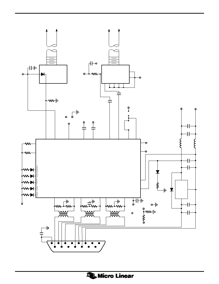
Figure 1. ML4668 Schematic Diagram
FIBER OPTIC RCVR
FIBER OPTIC CABLE
FIBER OPTIC CABLE
FIBER OPTIC
TRANSMITTER
ML4668
LM340
GND
AULCP≠
AULCP+
AULTX≠
AULTX+
1
2
3
4
5
6
7
8
9
10
11
12
13
14
15
CHASSIS REF
AULRX≠
AULRX+
AULPWR+
AULPWR≠
CI
D0
D1
8
7
5
4
2
11
6
15
13
12
10
9
360
360
7
10
39
11
2
360
360
COL≠
COL+
Tx≠
Tx+
Rx≠
Rx+
SQE
XMT
RCV
CLSN
JAB
LMON
RRSET
RTSET
TxOUT
15
16
1
2
8
14
ALL
510
RP1
61.9k
115
13
12
TxV
CC
LBDIS
C
TIMER
V
DC
V
IN
+
V
IN
≠
V
REF
V
THADJ
V
CC
18
17
8
4
21
26
25
22
23
+5V
+5V
+5V
9
19, 20
24
27
≠V
RF
+V
RF
0.1
510
RP1
D1
VR1
0.1µ
33µ
+
4.7µ
+
+
+
0.1µ
4.7µH
4.7µH
4.7
0.1
+V
RF
≠V
RF
IN
OUT
Q1
≠V
RF
+V
RF
≠V
RF
≠V
RF
+V
RF
0.01
2
1
4
5
8
73
0.01
R17
10
0.1µF
≠V
RF
6
3
2,6,7
+5V
0.1µF
1k
6
3K
5K
0.1
0.05
39
0.1
µ
F
5
3
HP HFBR1414
OR
OPTEK
OPC1414
HP HFBR2416
OR
OPTEK
OPC2416
7
ML4668
SYSTEM DESCRIPTION
Figure 1 shows a schematic diagram of the ML4668 in an
internal or external 10BASE-FL MAU. On one side of the
transceiver is the AU interface and the other is the fiber
optic interface. The AU interface is AC coupled when
used in an external transceiver or an internal transceiver.
The AU interface for an external transceiver includes
isolation transformers, some biasing resistors, and a
voltage regulator for power.
The fiber optic side of the transceiver requires an external
fiber optic transmitter and fiber optic receiver. The
transmitter uses a current driven output that directly drives
the fiber optic transmitter. The receive side of the
transceiver accepts the data after passing through a fiber
optic receiver, which consists of a module containing a
pin diode and a transimpedance amplifier.
AU INTERFACE
The AU interface consists of 3 pairs of signals: DO, CI and
DI (Figure 1). The DO pair contains transmit data from the
DTE which is received by the transceiver and sent out
onto the fiber optic cable. The DI pair contains valid data
that has been either received from the fiber optic cable or
looped back from the DO, and output through the DI pair
to the DTE. The CI pair indicates whether a collision has
occurred. It is an output that oscillates at 10MHz if a
collision, Jabber or SQE Test has taken place, otherwise it
remains idle.
When the transceiver is external, these three pairs are AC
coupled through isolation transformers, while an internal
transceiver may be capacitively coupled. Tx+, Tx≠ is
internally DC biased (shifted up in voltage) for the proper
common mode input voltage.
The two 39
1% resistors (or one 78
1% resistor) tied to
the Tx+ and Tx≠ pins will provide the proper termination.
The CI and DI pair, which are output from the transceiver
to the AUI cable, require 360
pull down resistors when
terminated with a 78
load. However, on a DTE card, CI
and DI do not need 78
terminating resistors. This also
means that the pull down resistors on CI and DI can be
1k
or greater depending upon the particular Manchester
encoder/decoder chip used. Using higher value pull down
resistors as in a DTE card will save power. Refer to
Application Note 13 for a more detailed explanation of
the AUI pull-down resistors.
The AUI drivers are capable of driving the full 50 meters
of cable length and have a rise and fall time of typically
4ns. In the idle state, the outputs go to the same voltage to
prevent DC standing current in the isolation transformers.
TRANSMISSION
The transmit function consists of detecting the presence of
data from the AUI DO input (Tx+, Tx≠) and driving that
data onto the fiber optic LED transmitter. A positive signal
on the Tx+ lead relative to the Tx≠ lead of the DO circuit
will result in no current, hence the fiber optic LED is in a
low light condition. When Tx+ is more negative than Tx≠,
the ML4668 will sink current into the chip and the fiber
optic LED will light up.
Before data will be transmitted onto the fiber optic cable
from the AUI interface, it must exceed the squelch
requirements for the DO pair. The Tx squelch circuit
serves the function of preventing any noise from being
transmitted onto the fiber. This circuit rejects signals with
pulse widths less than typically 20ns (negative going), or
with levels less than ≠250mV. Once Tx squelch circuit has
unsquelched, it looks for the start of idle signal to turn on
the squelch circuit again. The transmitter turns on the
squelch again when it receives an input signal at Tx+, Tx≠
that is more positive than ≠250mV for more than
approximately 180ns.
At the start of a packet transmission, no more than 2 bits
are received from the DO circuit, and are not transmitted
onto the fiber optic cable. The difference between start-up
delays (bit loss plus steady-state propagation delay) for
any two packets that are separated by 9.6
µ
s or less will
not exceed 200ns.
FIBER OPTIC LED DRIVER
The output stage of the transmitter is a current mode
switch which develops the output light by sinking current
through the LED into the TxOUT pin. Once the current
requirement for the LED is determined, the RTSET resistor
is selected. The following equation is used to select the
correct RTSET resistor:
RTSET= 52mA
I
OUT
115
The ML4668 transmitter output will drive up to 100mA,
which requires RTSET to equal 60
. The transmitter enters
the idle state when it detects start of idle on Tx+ and Tx≠
input pins. After detection, transmitter switches to a 1MHz
output idle signal.
The output current is switched through the TxOUT pin
during the on cycle and the V
CC
Tx pin during the off cycle
as shown in figure 2. Since the sum of the current in these
two pins is constant, V
CC
Tx should be connected as close
as possible to the V
CC
connection for the LED.
If not driving an optical LED directly, a differential output
can be generated by tying resistors from V
CC
Tx and
TxOUT to V
CC
as shown in figure 3. The minimum
voltage on these two pins should not be less than
V
CC
≠ 2V.
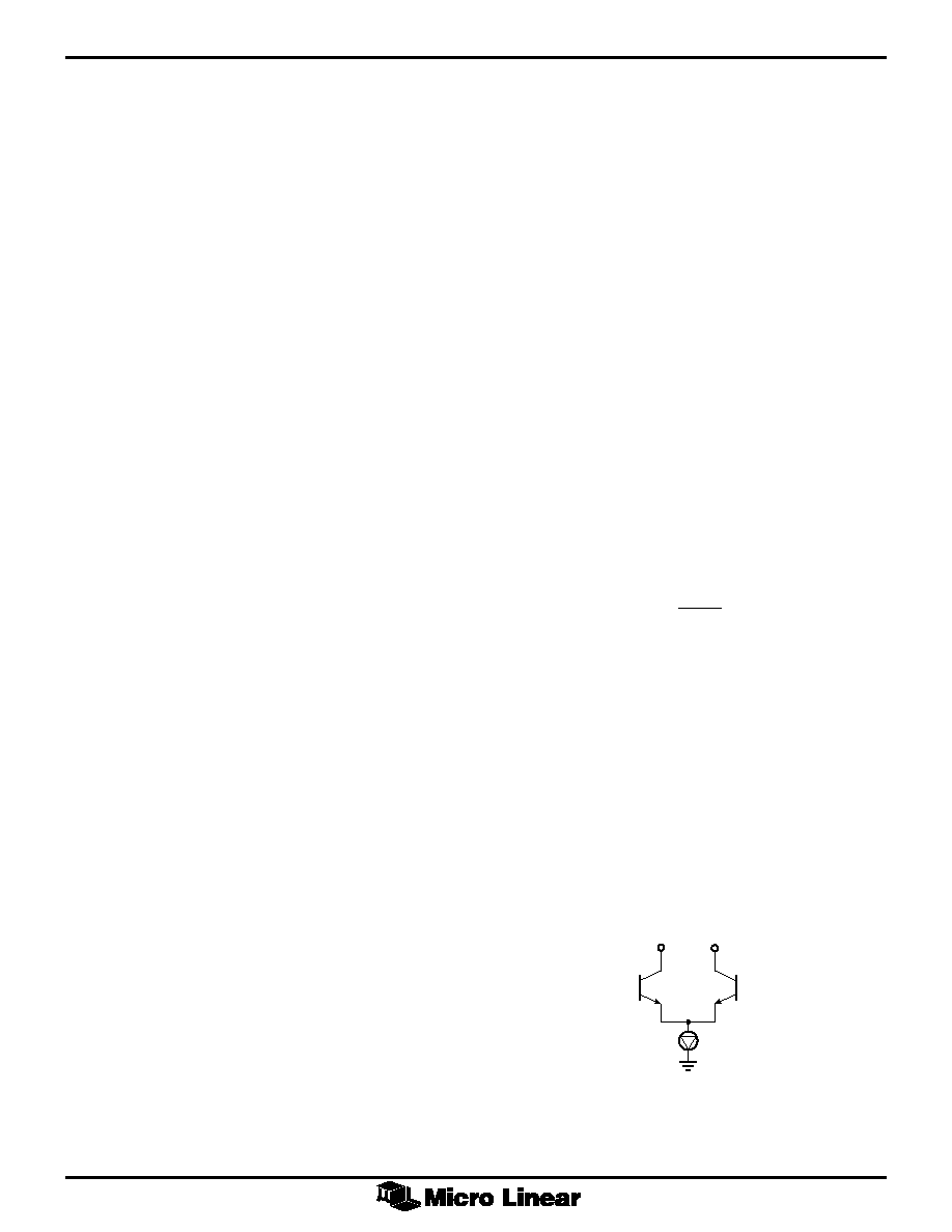
V
CC
Tx
TxOUT
I
OUT
Figure 2. Fiber Optic LED Driver Structure.
8
ML4668
V
CC
Tx
TxOUT
V
CC
51
51
51
RTSET = 560
I
OUT
= 15.9mA
ECL
Figure 3. Converting Optical LED Driver Output to
Differential ECL.
RECEPTION
The input to the transceiver comes from a fiber optic
receiver (Figure 1). At the start of packet reception no
more than 2.7 bits are received from the fiber cable, and
are not transmitted onto the DI circuit. The receive
squelch will reject frequencies lower than 2.51MHz.
While in the unsquelch state, the receive squelch circuit
looks for the start of idle signal at the end of the packet.
Start of idle occurs when the input signal remains idle for
more than 160ns. When start of idle is detected, the
receive squelch circuit returns to the squelch state and the
start of idle signal is output on the DI circuit (Rx+, Rx≠).
COLLISION
Whenever the receiver and the transmitter are active at
the same time the chip will activate the collision output,
except when loopback is disabled (LBDIS = V
CC
). The
collision output is a differential square wave matching the
AUI specifications and capable of driving a 78
load. The
frequency of the square wave is 10MHz
±
15% with a 60/
40 to 40/60 duty cycle. The collision oscillator also is
activated during SQE Test and Jabber.
LOOPBACK
The loopback function emulates a 10BASE-T transceiver
whereby the transmit data sent by the DTE is looped back
over the AUI receive pair. Some LAN controllers use this
loopback information to determine whether a MAU is
connected by monitoring the carrier sense while
transmitting. The software can use this loopback
information to determine whether a MAU is connected to
the DTE by checking the status of carrier sense after each
packet transmission.
When data is received by the chip while transmitting, a
collision condition exits. This will cause the collision
oscillator to turn on and the data on the DI pair will
follow V
IN
+, V
IN
≠. After a collision is detected, the
collision oscillator will remain on until either DO or
V
IN
+, V
IN
≠ go idle.
Loopback can be disabled by strapping LBDIS to V
CC
.
In this mode the chip operates as a full duplex transmitter
and receiver, and collision detection is disabled. A
loopback through the transceiver can be accomplished by
tying the fiber transmitter to the receiver.
SQE TEST FUNCTION (SIGNAL QUALITY ERROR)
The SQE test function allows the DTE to determine
whether the collision detect circuitry is functional. After
each transmission, during the inter packet gap time, the
collision oscillator will be activated for typically 1
µ
s. The
SQE test will not be activated if the chip is in the low light
state, or the jabber on state.
For SQE to operate, the SQEN pin must be tied to V
CC
.
This allows the MAU to be interfaced to a DTE. The SQE
test can be disabled by tying the SQEN pin to ground, for
a repeater interface.
JABBER FUNCTION REQUIREMENTS
The Jabber function prevents a babbling transmitter from
bringing down the network. Within the transceiver is a
Jabber timer that starts at the beginning of each
transmission and resets at the end of each transmission. If
the transmission last longer than 20ms the Jabber logic
disables the transmitter and turns on the collision signal
COL+, COL≠. When Tx+ and Tx≠ finally go idle, a second
timer measures 0.5 seconds of idle time before the
transmitter is enabled and collision is turned off. Even
though the transmitter is disabled during Jabber, the 1MHz
idle signal is still transmitted.
LED DRIVERS
The ML4668 has five LED drivers. The LED driver pins are
active low, and the LEDs are normally off (except for
LMON). The LEDs are tied to their respective pins through
a 500
resistor to 5V.
The
XMT, RCV and CLSN pins have pulse stretchers on
them which enables the LEDs to be visible. When
transmission or reception occurs, the LED
XMT, RCV or
CLSN status pins will activate low for several
milliseconds. If another transmit, receive or collision
conditions occurs before the timer expires, the LED timer
will reset and restart the timing. Therefore rapid events
will leave the LEDs continuously on. The
JAB and LMON
LEDs do not have pulse stretchers on them since their
conditions occur long enough for the eye to see.
LOW LIGHT CONDITION
The
LMON LED output is used to indicate a low light
condition.
LMON is activated low when both the receive
power exceeds the Link Monitor threshold and there are
transitions on V
IN
+, V
IN
≠ less than 3
µ
s apart. If either one
of these conditions do not exist,
LMON will go high.
INPUT AMPLIFIER
The V
IN
+, V
IN
≠ input signal is fed into a limiting amplifier
with a gain of about 100 and input resistance of 1.3k
.
Maximum sensitivity is achieved through the use of a DC
restoration feedback loop and AC coupling the input.
When AC coupled, the input DC bias voltage is set by an
on-chip network at about 1.7V. These coupling capacitors,
in conjunction with the input impedance of the amplifier,
establish a high pass filter with 3dB corner frequency, f
L
,
at
f =
1
2
300C
L
1
(1)

9
ML4668
Since the amplifier has a differential input, two capacitors
of equal value are required. If the signal driving the input
is single ended, one of the coupling capacitors can be tied
to AV
CC
(Figure 1).
The internal amplifier has a lowpass filter built-in to band
limit the input signal which in turn will improve the signal
to noise ratio.
Although the input is AC coupled, the offset voltage
within
the amplifier will be present at the amplifier's output. This
is represented by V
OS
in Figure 4. In order to reduce this
error, a DC feedback loop is incorporated. This negative
feedback loop nulls the offset voltage, forcing V
OS
to be
zero. Although the capacitor on V
DC
is non-critical, the
pole it creates can effect the stability of the feedback loop.
To avoid stability problems, the value of this capacitor
should be at least 10 times larger than the input coupling
capacitors.
V
OS
V
OUT
+
V
OUT
≠
Figure 4.
The comparator is a high-speed, differential zero crossing
detector that slices and accurately digitizes the receive
signal. The output of the comparator is fed in parallel into
both the receive squelch circuit and the loopback MUX.
LINK DETECT CIRCUIT AND LOW LIGHT
The link detect circuit monitors the input signal and
determines when the input falls below a preset voltage
level. When the input falls below a preset voltage, the
ML4668 goes into the Low Light state. In the Low Light
state the transmitter is disabled, but continues sending the
1MHz idle signal, the loopback is disabled, the receiver is
disabled, and the
LMON LED pin goes to high shutting off
the
LMON LED. To return to the Link Pass state, the
optical receiver power must be 20% higher than the shut-
off state. This built-in hysteresis adds stability to the Link
Monitor circuit. Once the receiver power threshold is
exceeded, the ML4668 waits 250ms to 750ms, then
checks to see that Tx+. Tx≠ is idle and no data is being
received before re-enabling the transmitter, receiver,
loopback circuit, and lighting up the
LMON LED.
The V
THADJ
pin is used to adjust the sensitivity of the
receiver. The ML4668 is capable of exceeding the
10BASE-FL specifications for sensitivity. The sensitivity is
dependent on the layout of the PC board. A good low
noise layout will exceed the 10BASE-FL specifications,
while a poor layout will fail to meet the sensitivity and
BER spec.
The threshold generator shifts the reference voltage at
V
THADJ
through a circuit which has a temperature
coefficient matching that of the limiting amplifier. The
relationship between the V
THADJ
and the V
TH
(the peak to
peak input threshold) is:
V
THADJ
= 408V
TH
(2)
In a 10BASE-FL receiver there must be less than 1 x 10
≠10
bit errors at a receive power level of ≠32.5dBm average.
One procedure to determine the sensitivity of a receiver is
to start at the lowest optical power level and gradually
increase the optical power until the BER is met. In this
case the Link Detect circuit must not disable the receiver
(i.e. V
THADJ
should be tied to Ground). Once the
sensitivity of the receiver is determined, V
THADJ
can be set
just above the power level that meets the BER
specification. This way the receiver will shut-off before the
BER is exceeded.
For 10BASE-FL V
THADJ
can be tied directly to V
REF
.
However if greater sensitivity is required the circuit in
figure 5 can be used to adjust the V
THADJ
voltage. Even if
V
REF
is tied to V
THADJ
, it is a good idea to layout a board
with these two resistors available. This will allow potential
future adjustments without board revisions.
The response time of the Link Detect circuit is set by the
C
TIMER
pin. Starting from the link off state the link can be
switched on if the input exceeds the set threshold for a
time given by:
T=
C
TIMER
◊
0.7V
A
700
µ
(3)
To switch the link from on to off, the above time will be
doubled. A value of 0.05
µ
F will meet to 10BASE-FL
specifications.
REF
THRESH
GEN
VREF
VTHADJ
R1
R2
Figure 5.

10
ML4668
Figure 7. Receive Timing
t
ROXDY
t
RXSDY
t
RXFX
t
AF
t
AR
V
IN
+
V
IN
≠
Rx+
Rx≠
VALID
DATA
VALID DATA
Figure 8. Collision Timing
TIMING DIAGRAMS
Figure 6. Transmit and Loopback Timing
t
TXNPW
t
TXODY
t
TXSDY
t
TXSOI
1
F
TXIDF
t
TXFPW
t
TXLP
VALID
DATA
VALID
IDLE
IDLE
DATA
VALID DATA
Tx+
Tx≠
TxOUT
Rx+
Rx≠
VALID
DATA
VALID
DATA
CS0
t
CPSQE
Tx+
Tx≠
V
IN
+
V
IN
≠
COL+
COL≠
Rx+
Rx≠
Tx
Tx
Rx
Rx
Rx

11
ML4668
TIMING DIAGRAMS
Figure 10. Collision Timing
Figure 9. Collision Timing
Figure 11. Collision Timing
VALID
DATA
t
SQEXR
CS0
V
IN
+
V
IN
≠
Tx+
Tx≠
COL+
COL≠
Rx+
Rx≠
Rx
Rx
Rx
Tx
Tx
Tx
VALID
DATA
t
SQEXR
CS0
Tx+
Tx≠
V
IN
+
V
IN
≠
COL+
COL≠
Rx+
Rx≠
RxIN
RxIN
RxIN
RxIN
RxIN
VALID
DATA
VALID
DATA
t
CPSQE
CS0
V
IN
+
V
IN
≠
Tx+
Tx≠
COL+
COL≠
12
ML4668
TIMING DIAGRAMS
Figure 14. Jabber Timing
CS0
Tx+
Tx ≠
COL+
COL≠
VALID
DATA
VALID
DATA
t
JSQE
t
JAD
t
JRT
TxOUT
Figure 13. SQE Timing
t
SQETD
VALID DATA
t
SQEDY
CS0
TxOUT
COL+
COL≠
Figure 12. Collision Timing
COL+
COL≠
1
F
CLF

13
ML4668
Figure 17. LED Timing
Figure 16. LED Timing
t
LED
Tx+
Tx≠
XMT
Figure 15. LED Timing
t
LLPH
t
LLCL
V
IN
+
V
IN
≠
LMON
t
LED
V
IN
+
RCV
V
IN
≠

1
4
ML4668
ORDERING INFORMATION
PART NUMBER
TEMPERATURE
PACKAGE
ML4668CQ
0
∞
C to 70
∞
C
28-Pin PLCC (Q28)
Micro Linear reserves the right to make changes to any product herein to improve reliability, function or design.
Micro Linear does not assume any liability arising out of the application or use of any product described herein,
neither does it convey any license under its patent right nor the rights of others. The circuits contained in this
data sheet are offered as possible applications only. Micro Linear makes no warranties or representations as to
whether the illustrated circuits infringe any intellectual property rights of others, and will accept no responsibility
or liability for use of any application herein. The customer is urged to consult with appropriate legal counsel
before deciding on a particular application.
DS4668-01
2092 Concourse Drive
San Jose, CA 95131
Tel: 408/433-5200
Fax: 408/432-0295
PHYSICAL DIMENSIONS
inches (millimeters)
0.099 - 0.110
(2.51 - 2.79)
PIN 1 ID
SEATING PLANE
0.485 - 0.495
(12.32 - 12.57)
0.450 - 0.456
(11.43 - 11.58)
0.013 - 0.021
(0.33 - 0.53)
0.165 - 0.180
(4.06 - 4.57)
1
0.450 - 0.456
(11.43 - 11.58)
0.485 - 0.495
(12.32 - 12.57)
8
15
22
0.025 - 0.045
(0.63 - 1.14)
(RADIUS)
0.050 BSC
(1.27 BSC)
0.009 - 0.011
(0.23 - 0.28)
0.026 - 0.032
(0.66 - 0.81)
0.042 - 0.048
(1.07 - 1.22)
0.148 - 0.156
(3.76 - 3.96)
0.042 - 0.056
(1.07 - 1.42)
0.390 - 0.430
(9.90 - 10.92)
0.300 BSC
(7.62 BSC)
Package: Q28
28-Pin PLCC
© Micro Linear 1997
is a registered trademark of Micro Linear Corporation
Products described in this document may be covered by one or more of the following patents, U.S.: 4,897,611; 4,964,026; 5,027,116; 5,281,862; 5,283,483; 5,418,502; 5,508,570; 5,510,727; 5,523,940;
5,546,017; 5,559,470; 5,565,761; 5,592,128; 5,594,376; Japan: 2598946. Other patents are pending.