 | –≠–ª–µ–∫—Ç—Ä–æ–Ω–Ω—ã–π –∫–æ–º–ø–æ–Ω–µ–Ω—Ç: ML4770CS | –°–∫–∞—á–∞—Ç—å:  PDF PDF  ZIP ZIP |

July 2000
PRELIMINARY
ML4770
*
2 Cell, Adjustable Output, High Current
Boost Regulator with Load Disconnect
1
GENERAL DESCRIPTION
The ML4770 is a continuous conduction mode boost
regulator designed for DC to DC conversion in multiple
cell battery power systems. Continuous conduction allows
the regulator to maximize output current for a given
inductor. The maximum switching frequency can exceed
200kHz, allowing the use of small, low cost inductors.
The ML4770 is capable of start-up with input voltages as
low as 1.8V. The output voltage can be set anywhere
between 3.0V and 5.5V by an external resistor divider
connected to the SENSE pin.
An integrated synchronous rectifier eliminates the need
for an external Schottky diode and provides a lower
forward voltage drop, resulting in higher conversion
efficiency. In addition, low quiescent current and variable
frequency operation result in high efficiency even at light
loads. The ML4770 requires only a few external
components to build a very small regulator capable of
achieving conversion efficiencies approaching 85%.
The SHDN input allows the user to stop the regulator from
* Some Packages Are Obsolete
switching, and provides complete isolation of the load
from the battery.
BLOCK DIAGRAM
FEATURES
s
Guaranteed full load start-up and operation at
1.8V input
s
Continuous conduction mode for high output current
s
Pulse Frequency Modulation and internal synchronous
rectification for high efficiency
s
Isolates the load from the input during shutdown
s
Minimum external components
s
Low ON resistance internal switching FETs
s
Low supply current
s
Adjustable output voltage (3V to 5.5V)
VL2
5
VOUT
4
SENSE
6
+
≠
SHUTDOWN
CONTROL
7
SHDN
VIN
2
2.57V
START-UP
3
GND
VL1
1
SYNCHRONOUS
RECTIFIER
CONTROL
BOOST
CONTROL
SHDN
+
≠
+
≠
8
PWR GND
ML4770
2
PIN CONFIGURATION
PIN DESCRIPTION
PIN
NAME
FUNCTION
1
V
L1
Boost inductor connection
2
V
IN
Battery input voltage
3
GND
Ground
4
SENSE
Programming pin for setting the output
voltage
PIN
NAME
FUNCTION
5
V
OUT
Boost regulator output
6
V
L2
Boost inductor connection
7
SHDN
Pulling this pin to V
IN
shuts down the
regulator, isolating the load from the
input
8
PWR GND
Return for the NMOS output transistor
ML4770
8-Pin SOIC (S08)
1
2
3
4
8
7
6
5
VL1
VIN
GND
SENSE
PWR GND
SHDN
VL2
VOUT
TOP VIEW
ML4770
3
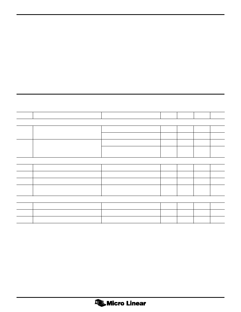
ELECTRICAL CHARACTERISTICS
Unless otherwise specified, V
IN
= Operating Voltage Range, T
A
= Operating Temperature Range (Note 1)
SYMBOL
PARAMETER
CONDITIONS
MIN
TYP
MAX
UNITS
SUPPLY
I
IN
V
IN
Current
V
IN
= V
OUT
- 0.2V, SHDN = 0V
3
6
µA
V
IN
= SHDN = 2.4V, V
OUT
= 0V
0.3
1
µA
I
OUT(Q)
V
OUT
Quiescent Current
SHDN = 0V
25
35
µA
V
IN
= SHDN = 2.4V,
14
20
µA
V
OUT
= V
OUT(NOM)
PFM REGULATOR
I
PEAK
I
L
Peak Current
1.1
1.3
1.6
A
V
SENSE
SENSE Comparator Threshold Voltage
2.52
2.57
2.62
V
Line Regulation
I
OUT
= 0, See Figure 1
4.95
5.05
5.15
V
Load Regulation
V
IN
= 2.4V, I
OUT
£ 220mA
4.85
4.95
5.15
V
See Figure 1
SHUTDOWN
V
IL
Input Low Voltage
0.5
V
V
IH
Input High Voltage
V
IN
- 0.5
V
Input Bias Current
-100
100
nA
Note 1:
Limits are guaranteed by 100% testing, sampling, or correlation with worst case test conditions.
ABSOLUTE MAXIMUM RATINGS
Absolute maximum ratings are those values beyond
which the device could be permanently damaged.
Absolute maximum ratings are stress ratings only and
functional device operation is not implied.
V
OUT ...............................................................................................
7V
Voltage on any other pin ..... GND - 0.3V to V
OUT
+ 0.3V
Peak Switch Current (I
PEAK
) ......................................... 2A
Average Switch Current (I
AVG
) ..................................... 1A
Junction Temperature ............................................. 150∫C
Storage Temperature Range .................... ≠65∫C to 150∫C
Lead Temperature (Soldering, 10 sec) ................... 260∫C
Thermal Resistance (
q
JA
) .................................. 160∫C/W
OPERATING CONDITIONS
Temperature Range
ML4770CS-X ............................................. 0∫C to 70∫C
ML4770ES-X ........................................... -20∫C to 70∫C
V
IN
Operating Range ....................... 1.8V to V
OUT
- 0.2V
V
OUT
Operating Range ............................... 3.0V to 5.5V

ML4770
4
Q1 ON
Q2 OFF
Q1 OFF
Q2 ON
IL
VL2
IL(MAX)
ISET
VOUT
0
0
Figure 1. Application Test Circuit
Figure 3. Inductor Current and Voltage Waveforms
Figure 2. PFM Regulator Block Diagram
VL2
5
VOUT
6
+
≠
SHUTDOWN
CONTROL
7
SHDN
VIN
2
2.57V
START-UP
3
GND
VL1
1
SYNCHRONOUS
RECTIFIER
CONTROL
BOOST
CONTROL
SHDN
+
≠
+
≠
8
PWR GND
A1
A2
A3
Q1
Q2
Q3
VOUT
4
SENSE
COUT
R1
R2
IL
ISET
RSENSE
ML4770
IOUT
100µF
100µF
VIN
27µH
(Sumida CD75)
VL1
VIN
GND
SENSE
PWR GND
SHDN
VL2
VOUT
268k
259k
VIN
ML4770
5
FUNCTIONAL DESCRIPTION
The ML4770 combines a unique form of current mode
control with a synchronous rectifier to create a boost
converter that can deliver high currents while maintaining
high efficiency. Current mode control allows the use of a
very small high frequency inductor and output capacitor.
Synchronous rectification replaces the conventional
external Schottky diode with an on-chip P-channel
MOSFET to reduce losses, eliminate an external
component, and provide the means for load disconnect.
Also included on-chip are an N-channel MOSFET main
switch and current sense resistor.
REGULATOR OPERATION
The ML4770 is a variable frequency, current mode
switching regulator. Its unique control scheme converts
efficiently over more than three decades of load current.
A block diagram of the boost converter including the key
external components is shown in Figure 2.
Error amp A3 converts deviations in the desired output
voltage to a small current, I
SET
. The inductor current is
measured through a current sense resistor (R
SENSE
) which
is amplified by A1. The boost control block matches the
average inductor current to a multiple of the I
SET
current
by switching Q1 on and off. The peak inductor current is
limited by the controller to about 1.3A.
At light loads, I
SET
will momentarily reach zero after an
inductor discharge cycle, causing Q1 to stop switching.
Depending on the load, this idle time can extend to
tenths of a second. When the circuit is not switching, only
25µA of supply current is drawn from the output. This
allows the part to remain efficient even when the load
current drops below 250µA.
Amplifier A2 and the PMOS transistor Q2 work together
to form a low drop diode. When transistor Q1 turns off,
the current flowing in the inductor causes V
L2
to go high.
As the voltage on V
L2
rises above V
OUT
, amplifier A2
allows the PMOS transistor Q2 to turn on. In
discontinuous operation, (where I
L
always returns to zero),
A2 uses the resistive drop across the PMOS switch Q2 to
sense zero inductor current and turns the PMOS switch
off. In continuous operation, the PMOS turn off point is
independent of A2 and is determined by the boost control
circuitry.
Typical inductor current and voltage waveforms are
shown in Figure 3.
SHUTDOWN
The ML4770 output can be shut down by pulling the
SHDN pin high (to V
IN
). When SHDN is high, the
regulator stops switching, the control circuitry is powered
down, and the body diode of the PMOS synchronous
rectifier is disconnected from the output. By switching
Q1, Q2, and Q3 off, the load is isolated from the input.
This allows the output voltage to be independent of the
input while in shutdown.
DESIGN CONSIDERATIONS
OUTPUT CURRENT CAPABILITY
The maximum current available at the output of the
regulator is related to the maximum inductor current by
the ratio of the input to output voltage and the conversion
efficiency. The maximum inductor current is limited by
the boost controller to about 1.0A. The conversion
efficiency is determined mainly by the internal switches
as well as the external components, but can be estimated
at about 80%. The maximum output current can be
determined by using the typical performance curves
shown in Figures 4 and 5, or by calculation using the
following equation:
I
V
V
V
A
OUT MAX
IN MIN
OUT
OUT
(
)
(
)
.
.
.
=
+
!
"
$
#
#
-
0 0972
0 486
0 144
1
6
2
7
(1)
Since the maximum output current is based on when the
inductor current goes into current limit, it is not
recommended to operate the ML4770 at the maximum
output current continuously. Applications that have high
transient load currents should be evaluated under worst
case conditions to determine suitability.
INDUCTOR SELECTION
The ML4770 is able to operate over a wide range of
inductor values. A value of 10µH is a good choice, but
any value between 5µH and 33µH is acceptable. As the
inductor value changes, the control circuitry will
automatically adjust to keep the inductor current under
control. Choosing an inductance value of less than 10µH
will reduce the component's footprint, but the efficiency
and maximum output current may drop.
It is important to use an inductor that is rated to handle
1.5A peak currents without saturating. Also look for an
inductor with low winding resistance. A good rule of
thumb is to allow 5 to 10m
W of resistance for each 1µH of
inductance.
The final selection of the inductor will be based on trade-
offs between size, cost and efficiency. Inductor tolerance,
core and copper loss will vary with the type of inductor
selected and should be evaluated with a ML4770 under
worst case conditions to determine its suitability.
Several manufacturers supply standard inductance values
in surface mount packages:
Coilcraft
(847) 639-6400
Coiltronics
(561) 241-7876
Dale
(605) 665-9301
Sumida
(847) 956-0666

ML4770
6
DESIGN CONSIDERATIONS
(Continued)
Figure 4. I
OUT
vs. V
IN
Using the Circuit of Figure 8
Figure 5. Efficiency vs. I
OUT
Using the Circuit of Figure 8
1000
800
600
400
200
0
I OUT
(mA)
VIN (V)
1.5
2.5
3.5
5.5
4.5
VOUT = 3V
VOUT = 5.5V
90
80
70
60
EFFICIENCY (%)
IOUT (mA)
1
10
100
1000
VOUT = 3V
VOUT = 5.5V
VIN = 2.4V
Figure 6. Input Leakage vs. V
IN
in Shutdown
Figure 7. No Load Input Current vs. V
IN
350
300
250
200
150
100
50
0
I IN
(nA)
VIN (V)
1.0
3.0
5.0
7.0
160
120
80
40
0
I IN
(µA)
VIN (V)
1.5
2.5
3.5
5.5
4.5
VOUT = 3V
VOUT = 5.5V
OUTPUT CAPACITOR
The output capacitor filters the pulses of current from the
switching regulator. Since the switching frequency will
vary with inductance, the minimum output capacitance
required to reduce the output ripple to an acceptable
level will be a function of the inductor used. Therefore, to
maintain an output voltage with less than 100mV of ripple
at full load current, use the following equation:
C
L
V
OUT
OUT
=
44
(2)
The output capacitor's Equivalent Series Resistance (ESR)
and Equivalent Series Inductance (ESL), also contribute to
the ripple. Just after the Q1 turns off, the current in the
output capacitor ramps quickly to between 0.5A and
1.3A. This fast change in current through the capacitor's
ESL causes a high frequency (5ns) spike to appear on the
output. After the ESL spike settles, the output still has a
ripple component equal to the inductor discharge current
times the ESR. To minimize these effects, choose an
output capacitor with less than 10nH of ESL and less than
100m
W of ESR.
Suitable tantalum capacitors can be obtained from the
following vendors:
AVX
(207) 282-5111
Kemet
(846) 963-6300
Sprague
(207) 324-4140
ML4770
7
DESIGN CONSIDERATIONS
(Continued)
In applications where the ML4770 is operated at or near
the maximum output current, it is recommended to add a
10nF to 100nF ceramic capacitor from V
OUT
to GND. The
optimum value of the high frequency bypass capacitor is
dependent on the layout and the value of the bulk output
capacitor selected.
INPUT CAPACITOR
Due to the high input current drawn at startup and
possibly during operation, it is recommended to decouple
the input with a capacitor with a value of 47µF to 100µF.
This filtering prevents the input ripple from affecting the
ML4770 control circuitry, and also improves the
efficiency by reducing the I
2
R losses during the charge
cycle of the inductor. Again, a low ESR capacitor (such as
tantalum) is recommended.
It is also recommended that low source impedance
batteries be used. Otherwise, the voltage drop across the
source impedance during high input current situations will
cause the ML4770 to fail to start up or to operate
unreliably. In general, for two cell applications the source
impedance should be less than 200m
W, which means that
small alkaline cells should be avoided.
SHUTDOWN
The input levels of the SHDN pin are CMOS compatible.
To guarantee proper operation, SHDN must be pulled to
within 0.5V of GND or V
IN
to prevent excessive power
dissipation and possible oscillations.
SETTING THE OUTPUT VOLTAGE
The adjustable output of the ML4770 requires an external
feedback resistor divider to set V
OUT
. The output voltage
can be determined from the following equation:
V
R
R2
R2
OUT
=
+
257
1
.
(
)
(3)
where R1 and R2 are connected as shown in Figure 2. The
value of R2 should be 250k
W or less to minimize bias
current errors. Choose an appropriate value for R2 and
calculate R1.
LAYOUT
Good layout practices will ensure the proper operation of
the ML4770. Some layout guidelines follow:
∑ Use adequate ground and power traces or planes
∑ Keep components as close as possible to the ML4770
∑ Use short trace lengths from the inductor to the V
L1
and
V
L2
pins and from the output capacitor to the V
OUT
pin
LAYOUT
(Continued)
∑ Use a single point ground for the ML4770 PWR GND
pin and the input and output capacitors, and connect
the GND pin to PWR GND using a separate trace
∑ Separate the ground for the converter circuitry from the
ground of the load circuitry and connect at a single
point
∑ Route the feedback trace away from the V
L2
trace to
avoid noise pickup
∑ Route the high frequency bypass capacitor from a
V
OUT
location near the output voltage setting resistor
to the GND pin
DESIGN EXAMPLE
In order to design a boost converter using the ML4770,
it is necessary to define the values of a few parameters.
For this example, assume that V
IN
= 3.0V to 3.6V,
V
OUT
= 5.0V, and I
OUT(MAX)
= 400mA.
First, it must be determined whether the ML4770 is
capable of delivering the output current. This is done
using Equation 1:
I
A
mA
OUT MAX
(
)
.
.
.
=
+
!
"
$
#
-
=
3
5
0 0972 5
0 486
0 144
439
0
5
2
7
Next, select an inductor:
As previously mentioned, it is the recommended
inductance is 10µH. Make sure that the peak current
rating of the inductor is at least 1.5A, and that the DC
resistance of the inductor is in the range of 50 to 100m
W.
Finally, the value of the output capacitor is determined
using Equation 2:
C
H
V
F
OUT
=
=
44 10
5 0
88
m
m
.
The closest standard value would be a 100µF capacitor
with an ESR rating of 100m
W. If such a low ESR value
cannot be found, two 47µF capacitors in parallel could
also be used. Since the 400mA output current is close to
the 439mA maximum, a 10nF capacitor from V
OUT
to
GND is recommended.
Finally, the values of R1 and R2 are calculated using
equation 3. Assuming R2 = 250k
W:
R
V
k
k
k
1
50
257
250
250
236
=
-
=
.
.
W
W
W
The complete circuit is shown in Figure 8. As mentioned
previously, the use of an input supply bypass capacitor is
strongly recommended.
ML4770
8
© Micro Linear 1997. is a registered trademark of Micro Linear Corporation. All other trademarks are the
property of their respective owners.
Products described herein may be covered by one or more of the following U.S. patents: 4,897,611;
4,964,026; 5,027,116; 5,281,862; 5,283,483; 5,418,502; 5,508,570; 5,510,727; 5,523,940; 5,546,017;
5,559,470; 5,565,761; 5,592,128; 5,594,376; 5,652,479; 5,661,427; 5,663,874; 5,672,959; 5,689,167.
Japan: 2,598,946; 2,619,299; 2,704,176. Other patents are pending.
Micro Linear reserves the right to make changes to any product herein to improve reliability, function or
design. Micro Linear does not assume any liability arising out of the application or use of any product
described herein, neither does it convey any license under its patent right nor the rights of others. The circuits
contained in this data sheet are offered as possible applications only. Micro Linear makes no warranties or
representations as to whether the illustrated circuits infringe any intellectual property rights of others, and will
accept no responsibility or liability for use of any application herein. The customer is urged to consult with
appropriate legal counsel before deciding on a particular application.
3/27/98 Printed in U.S.A.
PHYSICAL DIMENSIONS
inches (millimeters)
ORDERING INFORMATION
PART NUMBER
TEMPERATURE RANGE
PACKAGE
ML4770CS (Obsolete)
0∞C to 70∞C
8-Pin SOIC (S08)
ML4770ES
-20∞C to 70∞C
8-Pin SOIC (S08)
SEATING PLANE
0.148 - 0.158
(3.76 - 4.01)
PIN 1 ID
0.228 - 0.244
(5.79 - 6.20)
0.189 - 0.199
(4.80 - 5.06)
0.012 - 0.020
(0.30 - 0.51)
0.050 BSC
(1.27 BSC)
0.015 - 0.035
(0.38 - 0.89)
0.059 - 0.069
(1.49 - 1.75)
0.004 - 0.010
(0.10 - 0.26)
0.055 - 0.061
(1.40 - 1.55)
8
0.006 - 0.010
(0.15 - 0.26)
0∫ - 8∫
1
0.017 - 0.027
(0.43 - 0.69)
(4 PLACES)
Package: S08
8-Pin SOIC
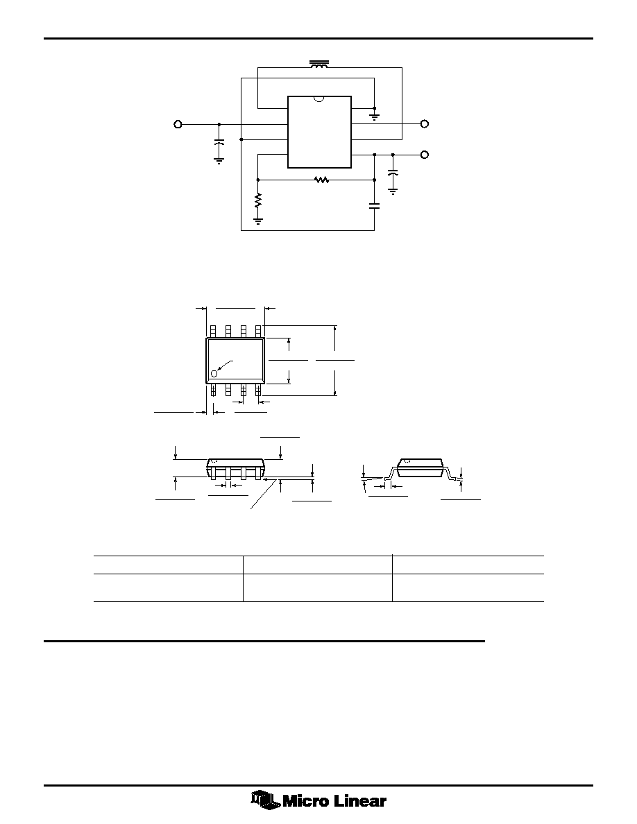
Figure 8. Design Example Schematic Diagram
ML4770
VOUT
COUT
100µF
10nF
CIN
100µF
VIN
10µH
(Sumida CD54)
VL1
VIN
GND
SENSE
PWR GND
SHDN
VL2
VOUT
R2
250k
R1
236k
SHUTDOWN
DS4770-01
2092 Concourse Drive
San Jose, CA 95131
Tel: (408) 433-5200
Fax: (408) 432-0295
www.microlinear.com