 | –≠–ª–µ–∫—Ç—Ä–æ–Ω–Ω—ã–π –∫–æ–º–ø–æ–Ω–µ–Ω—Ç: ML4803 | –°–∫–∞—á–∞—Ç—å:  PDF PDF  ZIP ZIP |

February 1999
PRELIMINARY
ML4803
8-Pin PFC and PWM Controller Combo
1
BLOCK DIAGRAM
GENERAL DESCRIPTION
The ML4803 is a space-saving controller for power factor
corrected, switched mode power supplies that offers very
low start-up and operating currents.
Power Factor Correction (PFC) offers the use of smaller,
lower cost bulk capacitors, reduces power line loading
and stress on the switching FETs, and results in a power
supply fully compliant to IEC1000-3-2 specifications. The
ML4803 includes circuits for the implementation of a
leading edge, average current "boost" type PFC and a
trailing edge, PWM.
The ML4803-1's PFC and PWM operate at the same
frequency, 67kHz. The PFC frequency of the ML4803-2 is
automatically set at half that of the 134kHz PWM. This
higher frequency allows the user to design with smaller
PWM components while maintaining the optimum
operating frequency for the PFC. An overvoltage
comparator shuts down the PFC section in the event of a
sudden decrease in load. The PFC section also includes
peak current limiting for enhanced system reliability.
FEATURES
s
Internally synchronized PFC and PWM in one 8-pin IC
s
Patented one-pin voltage error amplifier with advanced
input current shaping technique
s
Peak or average current, continuous boost, leading
edge PFC (Input Current Shaping Technology)
s
High efficiency trailing-edge current mode PWM
s
Low supply currents; start-up: 150µA typ., operating:
2mA typ.
s
Synchronized leading and trailing edge modulation
s
Reduces ripple current in the storage capacitor
between the PFC and PWM sections
s
Overvoltage, UVLO, and brownout protection
s
PFC V
CC
OVP with PFC Soft Start
ISENSE
3
VEAO
4
VDC
5
ILIMIT
6
GND
2
PWM OUT
8
PFC OUT
1
≠
+
≠
+
COMP
COMP
35µA
16.2V
17.5V
VCC
+
≠
COMP
+
≠
≠1V
SOFT START
PFC/PWM UVLO
DUTY CYCLE
LIMIT
OSCILLATOR
PFC ≠ 67kHz
PWM ≠ 134kHz
VREF
VREF
1.2V
26k
40k
M1
R1
C1
30pF
M2
M7
M3
M4
M6
PWM
CONTROL
LOGIC
≠
+
1.5V
DC ILIMIT
PFC ILIMIT
PWM COMPARATOR
VCC OVP
PFC OFF
ONE PIN ERROR AMPLIFIER
LEADING
EDGE PFC
TRAILING
EDGE PWM
+
≠
COMP
7V
+
≠
COMP
≠1
≠4
REF
VCC
7
PFC
CONTROL
LOGIC

ML4803
2
February 1999
PIN CONFIGURATION
PIN DESCRIPTION
PIN
NAME
FUNCTION
1
PFC OUT
PFC driver output
2
GND
Ground
3
I
SENSE
Current sense input to the PFC current
limit comparator
4
VEAO
PFC one-pin error amplifier input
PIN
NAME
FUNCTION
5
V
DC
PWM voltage feedback input
6
I
LIMIT
PWM current limit comparator input
7
V
CC
Positive supply (may require an
external shunt regulator)
8
PWM OUT PWM driver output
1
2
3
4
8
7
6
5
PFC OUT
GND
ISENSE
VEAO
PWM OUT
VCC
ILIMIT
VDC
TOP VIEW
ML4803
8-Pin PDIP (P08)
8-Pin SOIC (S08)

ML4803
3
February 1999
ABSOLUTE MAXIMUM RATINGS
Absolute maximum ratings are those values beyond which
the device could be permanently damaged. Absolute
maximum ratings are stress ratings only and functional
device operation is not implied.
I
CC
Current (average) ............................................. 40mA
V
CC
MAX ............................................................... 18.3V
I
SENSE
Voltage .................................................. -5V to 1V
Voltage on Any Other Pin ...... GND - 0.3V to V
CC
+ 0.3V
Peak PFC OUT Current, Source or Sink ....................... 1A
Peak PWM OUT Current, Source or Sink ..................... 1A
PFC OUT, PWM OUT Energy Per Cycle .................. 1.5µJ
Junction Temperature .............................................. 150∞C
Storage Temperature Range ..................... ≠65∞C to 150∞C
Lead Temperature (Soldering, 10 sec) ..................... 260∞C
Thermal Resistance (
q
JA
)
Plastic DIP ..................................................... 110∞C/W
Plastic SOIC ................................................... 160∞C/W
OPERATING CONDITIONS
Temperature Range
ML4803CX-X ............................................. 0∞C to 70∞C
ML4803IX-X ............................................-40∞C to 85∞C
ELECTRICAL CHARACTERISTICS
Unless otherwise specified, V
CC
= 15V, T
A
= Operating Temperature Range (Note 1)
SYMBOL
PARAMETER
CONDITIONS
MIN
TYP
MAX
UNITS
ONE-PIN ERROR AMPLIFIER
VEAO Output Current
T
A
= 25∫C, V
EAO
= 6V
33.5
35.0
36.5
µA
Line Regulation
10V < V
CC
< 15V, V
EAO
= 6V
0.1
0.3
µA
V
CC
OVP COMPARATOR
Threshold Voltage
T
A
= 0∫C to 70∫C
15.5
16.0
16.5
V
PFC I
LIMIT
COMPARATOR
Threshold Voltage
-0.9
-1
-1.15
V
Delay to Output
150
300
ns
DC I
LIMIT
COMPARATOR
Threshold Voltage
1.4
1.5
1.6
V
Delay to Output
150
300
ns
OSCILLATOR
Initial Accuracy
T
A
= 25∞C
62
67
74
kHz
Voltage Stability
10V < V
CC
< 15V
1
%
Temperature Stability
2
%
Total Variation
Over Line and Temp
60
67
74.5
kHz
Dead Time
PFC Only
0.3
0.45
0.65
µs
PFC
Minimum Duty Cycle
V
EAO
> 7.0V,I
SENSE
= -0.2V
0
%
Maximum Duty Cycle
V
EAO
< 4.0V,I
SENSE
= 0V
90
95
%
Output Low Impedance
8
15
W
Output Low Voltage
I
OUT
= -100mA
0.8
1.5
V
I
OUT
= ≠10mA, V
CC
= 8V
0.7
1.5
V

ML4803
4
February 1999
ELECTRICAL CHARACTERISTICS
(Continued)
SYMBOL
PARAMETER
CONDITIONS
MIN
TYP
MAX
UNITS
PFC (Continued)
Output High Impedance
8
15
W
Output High Voltage
I
OUT
= 100mA, V
CC
= 15V
13.5
14.2
V
Rise/Fall Time
C
L
= 1000pF
50
ns
PWM
Duty Cycle Range
TA = 0∫C to 70∫C, ML4803-2
0-43
0-47
0-50
%
TA = 0∫C to 70∫C, ML4803-1
0-49.5
0-50
%
Output Low Impedance
8
15
W
Output Low Voltage
I
OUT
= ≠100mA
0.8
1.5
V
I
OUT
= ≠10mA, V
CC
= 8V
0.7
1.5
V
Output High Impedance
8
15
W
Output High Voltage
I
OUT
= 100mA, V
CC
= 15V
13.5
14.2
V
Rise/Fall Time
C
L
= 1000pF
50
ns
SUPPLY
V
CC
Clamp Voltage (V
CCZ
)
I
CC
= 10mA
16.7
17.5
18.3
V
Start-up Current
V
CC
= 11V, C
L
= 0
0.2
0.4
mA
Operating Current
V
CC
= 15V, C
L
= 0
2.5
4
mA
Undervoltage Lockout Threshold
11.5
12
12.5
V
Undervoltage Lockout Hysteresis
2.4
2.9
3.4
V
Note 1:
Limits are guaranteed by 100% testing, sampling, or correlation with worst case test conditions.

ML4803
5
February 1999
FUNCTIONAL DESCRIPTION
The ML4803 consists of an average current mode boost
Power Factor Corrector (PFC) front end followed by a
synchronized Pulse Width Modulation (PWM) controller. It
is distinguished from earlier combo controllers by its low
pin count, innovative input current shaping technique, and
very low start-up and operating currents. The PWM section
is dedicated to peak current mode operation. It uses
conventional trailing-edge modulation, while the PFC uses
leading-edge modulation. This patented Leading Edge/
Trailing Edge (LETE) modulation technique helps to
minimize ripple current in the PFC DC buss capacitor.
The ML4803 is offered in two versions. The ML4803-1
operates both PFC and PWM sections at 67kHz, while the
ML4803-2 operates the PWM section at twice the
frequency (134kHz) of the PFC. This allows the use of
smaller PWM magnetics and output filter components,
while minimizing switching losses in the PFC stage.
In addition to power factor correction, several protection
features have been built into the ML4803. These include
soft start, redundant PFC over-voltage protection, peak
current limiting, duty cycle limit, and under voltage
lockout (UVLO). See Figure 12 for a typical application.
DETAILED PIN DESCRIPTIONS
V
EAO
This pin provides the feedback path which forces the PFC
output to regulate at the programmed value. It connects to
programming resistors tied to the PFC output voltage and
is shunted by the feedback compensation network.
I
SENSE
This pin ties to a resistor or current sense transformer
which senses the PFC input current. This signal should be
negative with respect to the IC ground. It internally feeds
the pulse-by-pulse current limit comparator and the
current sense feedback signal. The I
LIMIT
trip level is ≠1V.
The I
SENSE
feedback is internally multiplied by a gain of
four and compared against the internal programmed ramp
to set the PFC duty cycle. The intersection of the boost
inductor current downslope with the internal
programming ramp determines the boost off-time.
V
DC
This pin is typically tied to the feedback opto-collector. It
is tied to the internal 5V reference through a 26k
W resistor
and to GND through a 40k
W resistor.
I
LIMIT
This pin is tied to the primary side PWM current sense
resistor or transformer. It provides the internal pulse-by
pulse-current limit for the PWM stage (which occurs at
1.5V) and the peak current mode feedback path for the
current mode control of the PWM stage. The current ramp
is offset internally by 1.2V and then compared against the
opto feedback voltage to set the PWM duty cycle.
PFC OUT and PWM OUT
PFC OUT and PWM OUT are the high-current power
drivers capable of directly driving the gate of a power
MOSFET with peak currents up to ±1A. Both outputs are
actively held low when V
CC
is below the UVLO threshold
level.
V
CC
V
CC
is the power input connection to the IC. The V
CC
start-
up current is 150µA . The no-load I
CC
current is 2mA. V
CC
quiescent current will include both the IC biasing currents
and the PFC and PWM output currents. Given the
operating frequency and the MOSFET gate charge (Qg),
average PFC and PWM output currents can be calculated
as I
OUT
= Qg x F. The average magnetizing current
required for any gate drive transformers must also be
included. The V
CC
pin is also assumed to be proportional
to the PFC output voltage. Internally it is tied to the
V
CC
OVP comparator (16.2V) providing redundant high-
speed over-voltage protection (OVP) of the PFC stage.
V
CC
also ties internally to the UVLO circuitry, enabling
the IC at 12V and disabling it at 9.1V. V
CC
must be
bypassed with a high quality ceramic bypass capacitor
placed as close as possible to the IC.
Good bypassing is critical to the proper operation of the
ML4803.
V
CC
is typically produced by an additional winding off
the boost inductor or PFC Choke, providing a voltage that
is proportional to the PFC output voltage. Since the
V
CC
OVP max voltage is 16.2V, an internal shunt limits
V
CC
overvoltage to an acceptable value. An external
clamp, such as shown in Figure 1, is desirable but not
necessary.
V
CC
is internally clamped to 16.7V minimum, 18.3V
maximum. This limits the maximum V
CC
that can be
applied to the IC while allowing a V
CC
which is high
Figure 1. Optional V
CC
Clamp
VCC
GND
1N4148
1N4148
1N5246B
ML4803
6
February 1999
RAMP
VEAO
TIME
VSW1
TIME
REF
EA
≠
+
≠
+
OSC
DFF
R
D
Q
Q
CLK
U1
RAMP
CLK
U4
U3
C1
RL
I4
SW2
SW1
+
DC
I1
I2
I3
VIN
L1
U2
Figure 2. Typical Trailing Edge Control Scheme.
enough to trip the V
CC
OVP. The max current through this
zener is 10mA. External series resistance is required in
order to limit the current through this Zener in the case
where the V
CC
voltage exceeds the zener clamp level.
GND
GND is the return point for all circuits associated with
this part. Note: a high-quality, low impedance ground is
critical to the proper operation of the IC. High frequency
grounding techniques should be used.
POWER FACTOR CORRECTION
Power factor correction makes a nonlinear load look like a
resistive load to the AC line. For a resistor, the current
drawn from the line is in phase with, and proportional to,
the line voltage. This is defined as a unity power factor is
(one). A common class of nonlinear load is the input of a
most power supplies, which use a bridge rectifier and
capacitive input filter fed from the line. Peak-charging
effect, which occurs on the input filter capacitor in such a
supply, causes brief high-amplitude pulses of current to
flow from the power line, rather than a sinusoidal current
in phase with the line voltage. Such a supply presents a
power factor to the line of less than one (another way to
state this is that it causes significant current harmonics to
appear at its input). If the input current drawn by such a
supply (or any other nonlinear load) can be made to
follow the input voltage in instantaneous amplitude, it
will appear resistive to the AC line and a unity power
factor will be achieved.
To hold the input current draw of a device drawing power
from the AC line in phase with, and proportional to, the
input voltage, a way must be found to prevent that device
from loading the line except in proportion to the
instantaneous line voltage. The PFC section of the
ML4803 uses a boost-mode DC-DC converter to
accomplish this. The input to the converter is the full wave
rectified AC line voltage. No filtering is applied following
the bridge rectifier, so the input voltage to the boost
converter ranges, at twice line frequency, from zero volts
to the peak value of the AC input and back to zero. By
forcing the boost converter to meet two simultaneous
conditions, it is possible to ensure that the current that the
converter draws from the power line matches the
instantaneous line voltage. One of these conditions is that
the output voltage of the boost converter must be set
higher than the peak value of the line voltage. A
commonly used value is 385VDC, to allow for a high line
of 270VAC
RMS
. The other condition is that the current that
the converter is allowed to draw from the line at any given
instant must be proportional to the line voltage.
Since the boost converter topology in the ML4803 PFC is
of the current-averaging type, no slope compensation is
required.
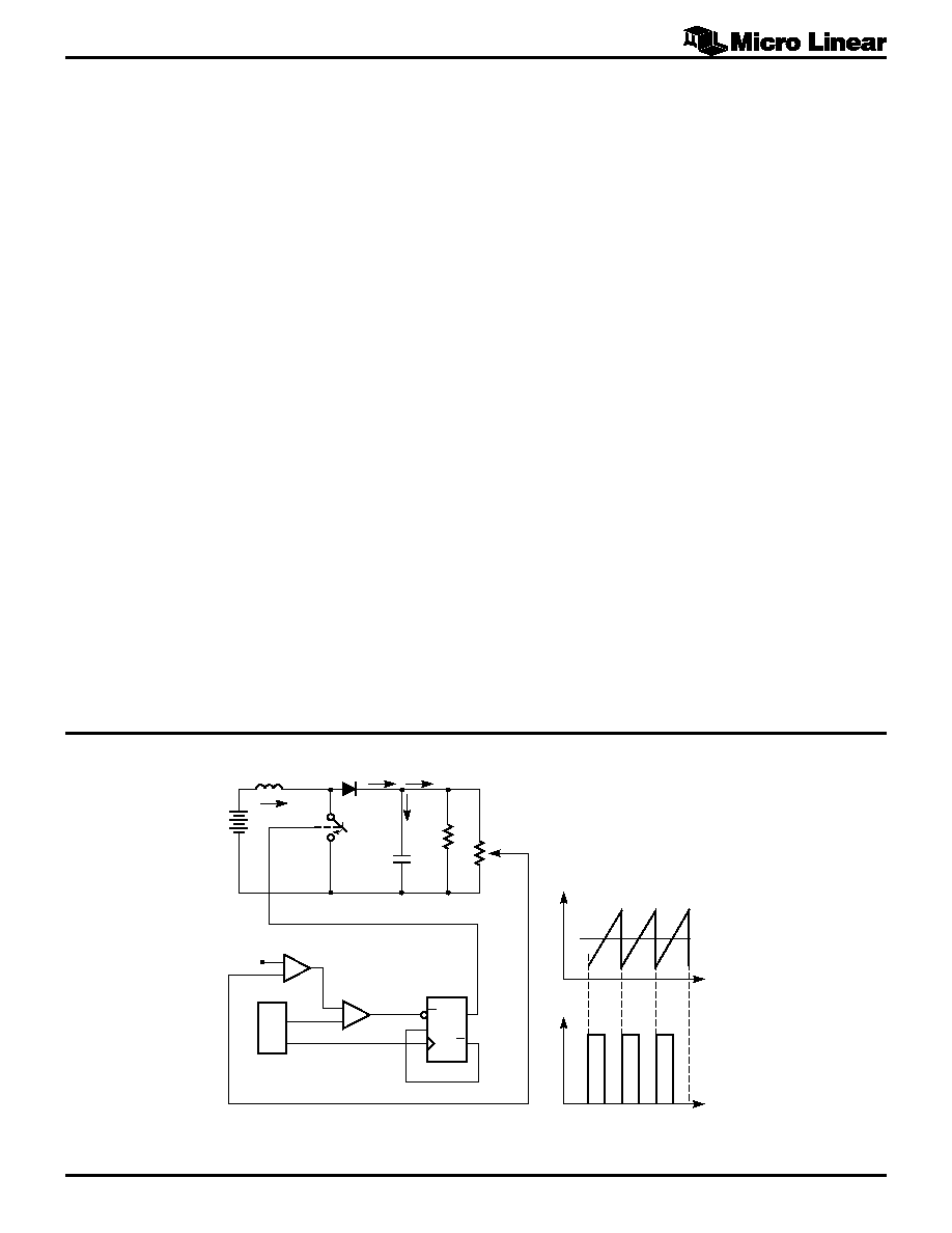
LEADING/TRAILING MODULATION
Conventional Pulse Width Modulation (PWM) techniques
employ trailing edge modulation in which the switch will
turn ON right after the trailing edge of the system clock.
The error amplifier output voltage is then compared with
the modulating ramp. When the modulating ramp reaches
the level of the error amplifier output voltage, the switch
will be turned OFF. When the switch is ON, the inductor
FUNCTIONAL DESCRIPTION
(Continued)

ML4803
7
February 1999
REF
EA
≠
+
≠
+
OSC
DFF
R
D
Q
Q
CLK
U1
RAMP
CLK
U4
U3
C1
RL
I4
SW2
SW1
+
DC
I1
I2
I3
VIN
L1
VEAO
CMP
U2
RAMP
VEAO
TIME
VSW1
TIME
Figure 3. Typical Leading Edge Control Scheme.
current will ramp up. The effective duty cycle of the
trailing edge modulation is determined during the ON
time of the switch. Figure 2 shows a typical trailing edge
control scheme.
In the case of leading edge modulation, the switch is
turned OFF right at the leading edge of the system clock.
When the modulating ramp reaches the level of the error
amplifier output voltage, the switch will be turned ON.
The effective duty-cycle of the leading edge modulation is
determined during the OFF time of the switch. Figure 3
shows a leading edge control scheme.
One of the advantages of this control technique is that it
requires only one system clock. Switch 1 (SW1) turns OFF
and Switch 2 (SW2) turns ON at the same instant to
minimize the momentary "no-load" period, thus lowering
ripple voltage generated by the switching action. With
such synchronized switching, the ripple voltage of the first
stage is reduced. Calculation and evaluation have shown
that the 120Hz component of the PFC's output ripple
voltage can be reduced by as much as 30% using this
method, substantially reducing dissipation in the high-
voltage PFC capacitor.
TYPICAL APPLICATIONS
ONE PIN ERROR AMP
The ML4803 utilizes a one pin voltage error amplifier in
the PFC section (VEAO). The error amplifier is in reality a
current sink which forces 35µA through the output
programming resistor. The nominal voltage at the VEAO
pin is 5V. The VEAO voltage range is 4 to 6V. For a
11.3M
W resistor chain to the boost output voltage and 5V
steady state at the VEAO, the boost output voltage would
be 400V.
PROGRAMMING RESISTOR VALUE
Equation 1 calculates the required programming resistor
value.
Rp
V
V
I
V
V
A
M
BOOST
EAO
PGM
=
-
=
-
=
400
50
35
113
.
.
µ
(1)
PFC VOLTAGE LOOP COMPENSATION
The voltage-loop bandwidth must be set to less than
120Hz to limit the amount of line current harmonic
distortion. A typical crossover frequency is 30Hz.
Equation 1, for simplicity, assumes that the pole capacitor
dominates the error amplifier gain at the loop unity-gain
frequency. Equation 2 places a pole at the crossover
frequency, providing 45 degrees of phase margin.
Equation 3 places a zero one decade prior to the pole.
Bode plots showing the overall gain and phase are shown
in Figures 5 and 6. Figure 4 displays a simplified model of
the voltage loop.
C
Pin
R
V
VEAO C
f
COMP
p
BOOST
OUT
=
◊
◊
◊
◊ ◊ ◊
2
2
1
6
(2)
C
W
M
V
V
F
Hz
COMP
=
¥
¥
¥
¥ ¥ ¥
300
113
400
0 5
220
2
30
2
.
.
W
m
p
0
5
C
nF
COMP
= 16
LEADING/TRAILING MODULATION
(Continued)

ML4803
8
February 1999
Figure 4. Voltage Control Loop
60
40
20
0
≠20
≠40
≠60
GAIN (dB)
FREQUENCY (Hz)
0.1
10
1000
1
100
Power Stage
Overall Gain
Compensation
Network Gain
0
50
100
150
200
PHASE (
∫
)
FREQUENCY (Hz)
0.1
1
10
1000
100
Power Stage
Overall
Compensation
Network
Figure 5. Voltage Loop Gain
Figure 6. Voltage Loop Phase
50
40
30
20
10
0
I RAMP
(µA)
VEAO (V)
0
2
7
5
1
3
6
4
FF @ ≠55∫C
TYP @ ≠55∫C
TYP @ 155∫C
SS @ 155∫C
TYP @ ROOM TEMP
Figure 7. Internal Ramp Current vs. V
EAO
R
f
C
COMP
COMP
=
¥ ¥ ¥
1
2
p
(3)
R
Hz
nF
k
COMP
=
¥
¥
=
1
6 28 30
16
330
.
W
C
f
R
ZERO
COMP
=
¥ ¥
¥
1
2
10
p
(4)
C
Hz
k
F
ZERO
=
¥
¥
=
1
6 28 3
330
0 16
.
.
W
m
INTERNAL VOLTAGE RAMP
The internal ramp current source is programmed by way of
the VEAO pin voltage. Figure 7 displays the internal ramp
current vs. the VEAO voltage. This current source is used
to develop the internal ramp by charging the internal
30pF +12/≠10% capacitor. See Figures 10 and 11. The
frequency of the internal programming ramp is set
internally to 67kHz.
PFC CURRENT SENSE FILTERING
In DCM, the input current wave shaping technique used
by the ML4803 could cause the input current to run away.
In order for this technique to be able to operate properly
under DCM, the programming ramp must meet the boost
inductor current down-slope at zero amps. Assuming the
programming ramp is zero under light load, the OFF-time
will be terminated once the inductor current reaches zero.
Subsequently the PFC gate drive is initiated, eliminating
the necessary dead time needed for the DCM mode. This
forces the output to run away until the V
CC
OVP shuts
down the PFC. This situation is corrected by adding an
TYPICAL APPLICATIONS
(Continued)
ML4803
ML4803
IVEAO
35µA
IOUT
VO
220µF
RLOAD
667
330k
11.3M
0.15µF
15nF
POWER
STAGE
COMPENSATION
VEAO
VEAO +
≠

ML4803
9
February 1999
TYPICAL APPLICATIONS
(Continued)
Figure 8. PFC Soft Start
Figure 9. I
SENSE
Offset for Light Load Conditions
offset voltage to the current sense signal, which forces the
duty cycle to zero at light loads. This offset prevents the
PFC from operating in the DCM and forces pulse-skipping
from CCM to no-duty, avoiding DMC operation. External
filtering to the current sense signal helps to smooth out
the sense signal, expanding the operating range slightly
into the DCM range, but this should be done carefully, as
this filtering also reduces the bandwidth of the signal
feeding the pulse-by-pulse current limit signal. Figure 9
displays a typical circuit for adding offset to I
SENSE
at
light loads.
PFC Start-Up and Soft Start
During steady state operation VEAO draws 35µA. At start-
up the internal current mirror which sinks this current is
defeated until V
CC
reaches 12V. This forces the PFC error
voltage to V
CC
at the time that the IC is enabled. With
leading edge modulation V
CC
on the VEAO pin forces
zero duty on the PFC output. When selecting external
compensation components and V
CC
supply circuits VEAO
must not be prevented from reaching 6V prior to V
CC
reaching 12V in the turn-on sequence. This will guarantee
that the PFC stage will enter soft-start. Once V
CC
reaches
12V the 35µA VEAO current sink is enabled. VEAO
compensation components are then discharged by way of
the 35µA current sink until the steady state operating point
is reached. See Figure 8.
PFC SOFT RECOVERY FOLLOWING V
CC
OVP
The ML4803 assumes that V
CC
is generated from a source
that is proportional to the PFC output voltage. Once that
source reaches 16.2V the internal current sink tied to the
VEAO pin is disabled just as in the soft start turn-on
sequence. Once disabled, the VEAO pin charges HIGH
by way of the external components until the PFC duty
cycle goes to zero, disabling the PFC. The V
CC
OVP resets
once the VCC discharges below 16.2V, enabling the
VEAO current sink and discharging the VEAO
compensation components until the steady state operating
point is reached. It should be noted that, as shown in
Figure 8, once the VEAO pin exceeds 6.5V, the internal
ramp is defeated. Because of this, an external Zener can
be installed to reduce the maximum voltage to which the
VEAO pin may rise in a shutdown condition. Clamping
the VEAO pin externally to 7.4V will reduce the time
required for the VEAO pin to recover to its steady state
value.
UVLO
Once V
CC
reaches 12V both the PFC and PWM are
enabled. The UVLO threshold is 9.1V providing 2.9V of
hysteresis.
GENERATING V
CC
An internal clamp limits overvoltage to V
CC
. This clamp
circuit ensures that the V
CC
OVP circuitry of the ML4803
will function properly over tolerance and temperature
while protecting the part from voltage transients. This
circuit allows the ML4803 to deliver 15V nominal gate
drive at PWM OUT and PFC OUT, sufficient to drive low-
cost IGBTs.
It is important to limit the current through the Zener to
avoid overheating or destroying it. This can be done with
a single resistor in series with the V
CC
pin, returned to a
bias supply of typically 14V to 18V. The resistor value
must be chosen to meet the operating current requirement
of the ML4803 itself (4.0mA max) plus the current
required by the two gate driver outputs.
V
CC
OVP
V
CC
is assumed to be a voltage proportional to the PFC
output voltage, typically a bootstrap winding off the boost
0
0
200ms/Div.
VBOOST
0
VOUT
VEAO
VCC
10V/div.
10V/div.
10V/div.
200V/div.
0
PFC
GATE
C23
0.01µF
CR16
1N4148
R29
20k
VCC
RTN
R28
20k
R4
1k
C16
1µF
C5
0.0082µF
R19
10k
ISENSE
R3
0.015
3W

ML4803
10
February 1999
inductor. The V
CC
OVP comparator senses when this
voltage exceeds 16V, and terminates the PFC output drive
while disabling the VEAO current sink. Once the VEAO
current sink is disabled, the VEAO voltage will charge
unabated, except for a diode clamp to V
CC
, reducing the
PFC pulse width. Once the V
CC
rail has decreased to
below 16.2V the VEAO sink will be enabled, discharging
external VEAO compensation components until the steady
state voltage is reached. Given that 15V on V
CC
corresponds to 400V on the PFC output, 16V on V
CC
corresponds to an OVP level of 426V.
COMPONENT REDUCTION
Components associated with the V
RMS
and I
RMS
pins of a
typical PFC controller such as the ML4824 have been
eliminated. The PFC power limit and bandwidth does vary
with line voltage. Double the power can be delivered from
a 220 V AC line versus a 110 V AC line. Since this is a
combination PFC/PWM, the power to the load is limited
by the PWM stage.
Figure 11. ML4803 PFC Control
Figure 10. Typical Peak Current Mode Waveforms
TYPICAL APPLICATIONS
(Continued)
VISENSE
VC1 RAMP
GATE
DRIVE
OUTPUT
CZERO
ISENSE
VC1
5V
VI SENSE
GATE
OUTPUT
RCOMP
RP
VOUT = 400V
VEAO
35µA
R1
4
+
≠
COMP
≠4
3
CCOMP
C1
30pF

ML4803
11
February 1999
Figure 12. Typical Application Circuit. Universal Input 240W 12V DC Output
BR1
600V
4A
LINE
NEUTRAL
F1 5A 250V
J1-1
J1-2
C19
4.7nF
250VAC
C20
4.7nF
250VAC
R24
470k
0.5W
TH1
10
5A
R3 0.15
3W
102T
L2
Q5
Q2
Q4
Q1
1000µH
R1
36
CR1 8A, 600V
CR7
CR3
CR18 51V
C26
0.01µF
500V
C18 4.7nF
CR2
30A, 60V
R36 220
L1 25µH
C29 0.01µF
CR2
30A
60V
C2
2200µF
C3
1µF
C1
220µF
450V
R2
L3
36
CR5
16V
0.5W
R22
10k
R8 36
R23
10k
R38 22
R30 200
C7
0.1µF
R27
20k
3W
R26
20k
3W
R10
0.75
3W
T2
T1
C23
0.01µF
CR4
CR11
CR10
CR12
CR9
R5 36
R11 150
Q3
R4 1k
ML4803
1
2
3
4
8
7
6
5
C15
0.015µF
C6
1µF
C5
8.2nF
C28
1µF
C9
1µF
C10
2.2nF
U2
4
5
1
2
2
3
1
R17 3.3k
R6 1.2k
C12 0.1µF
C25
0.01µF
500V
12V
J2-1
12VRET
J2-2
R18 1k
U3
CR8
L2
4T
CR15
1
10
3
4
R32 100
C27
0.01µF
R15
9.09k
7.0V
R21
10k
C14
4.7µF
C17
0.1µF
R16
2.37k
R13
5.62M
R7
10
CR16
IN4148
R12
5.62M
C4
0.47µF
250VAC
R14
150
2W
R37
330
R9
1.5k
C13 1nF
R31
10
C11
1000µF
C21
1µF
C22
1µF
R29 20k
R28
20k
R19
10k
PFC
GND
ISENSE
VEAO
PWM
VCC
ILIMIT
VDC
R20
510
R25
390k
C8
0.15µF
C16
0.01µF

ML4803
12
February 1999
PHYSICAL DIMENSIONS
inches (millimeters)
SEATING PLANE
0.240 - 0.260
(6.09 - 6.60)
PIN 1 ID
0.299 - 0.335
(7.59 - 8.50)
0.365 - 0.385
(9.27 - 9.77)
0.016 - 0.020
(0.40 - 0.51)
0.100 BSC
(2.54 BSC)
0.008 - 0.012
(0.20 - 0.31)
0.015 MIN
(0.38 MIN)
8
0∫ - 15∫
1
0.055 - 0.065
(1.39 - 1.65)
0.170 MAX
(4.32 MAX)
0.125 MIN
(3.18 MIN)
0.020 MIN
(0.51 MIN)
(4 PLACES)
Package: P08
8-Pin PDIP
SEATING PLANE
0.148 - 0.158
(3.76 - 4.01)
PIN 1 ID
0.228 - 0.244
(5.79 - 6.20)
0.189 - 0.199
(4.80 - 5.06)
0.012 - 0.020
(0.30 - 0.51)
0.050 BSC
(1.27 BSC)
0.015 - 0.035
(0.38 - 0.89)
0.059 - 0.069
(1.49 - 1.75)
0.004 - 0.010
(0.10 - 0.26)
0.055 - 0.061
(1.40 - 1.55)
8
0.006 - 0.010
(0.15 - 0.26)
0∫ - 8∫
1
0.017 - 0.027
(0.43 - 0.69)
(4 PLACES)
Package: S08
8-Pin SOIC

ML4803
13
February 1999
Micro Linear Corporation
2092 Concourse Drive
San Jose, CA 95131
Tel: (408) 433-5200
Fax: (408) 432-0295
www.microlinear.com
ORDERING INFORMATION
PART NUMBER
PFC/PWM FREQUENCY
TEMPERATURE RANGE
PACKAGE
ML4803CP-1
67kHz / 67kHz
0∞C to 70∞C
8-Pin PDIP (P08)
ML4803CS-1
67kHz / 67kHz
0∞C to 70∞C
8-Pin SOIC (S08)
ML4803IP-1
67kHz / 67kHz
-40∞C to 85∞C
8-Pin PDIP (P08)
ML4803IS-1
67kHz / 67kHz
-40∞C to 85∞C
8-Pin SOIC (S08)
ML4803CP-2
67kHz / 134kHz
0∞C to 70∞C
8-Pin PDIP (P08)
ML4803CS-2
67kHz / 134kHz
0∞C to 70∞C
8-Pin SOIC (S08)
ML4803IP-2
67kHz / 134kHz
-40∞C to 85∞C
8-Pin PDIP (P08)
ML4803IS-2
67kHz / 134kHz
-40∞C to 85∞C
8-Pin SOIC (S08)
© Micro Linear 1999.
is a registered trademark of Micro Linear Corporation. All other trademarks are the
property of their respective owners.
Products described herein may be covered by one or more of the following U.S. patents: 4,897,611; 4,964,026; 5,027,116;
5,281,862; 5,283,483; 5,418,502; 5,508,570; 5,510,727; 5,523,940; 5,546,017; 5,559,470; 5,565,761; 5,592,128; 5,594,376;
5,652,479; 5,661,427; 5,663,874; 5,672,959; 5,689,167; 5,714,897; 5,717,798; 5,742,151; 5,747,977; 5,754,012; 5,757,174;
5,767,653; 5,777,514; 5,793,168; 5,798,635; 5,804,950; 5,808,455; 5,811,999; 5,818,207; 5,818,669; 5,825,165; 5,825,223;
5,838,723; 5.844,378; 5,844,941. Japan: 2,598,946; 2,619,299; 2,704,176; 2,821,714. Other patents are pending.
Micro Linear makes no representations or warranties with respect to the accuracy, utility, or completeness of the contents
of this publication and reserves the right to make changes to specifications and product descriptions at any time without
notice. No license, express or implied, by estoppel or otherwise, to any patents or other intellectual property rights is granted
by this document. The circuits contained in this document are offered as possible applications only. Particular uses or
applications may invalidate some of the specifications and/or product descriptions contained herein. The customer is urged
to perform its own engineering review before deciding on a particular application. Micro Linear assumes no liability
whatsoever, and disclaims any express or implied warranty, relating to sale and/or use of Micro Linear products including
liability or warranties relating to merchantability, fitness for a particular purpose, or infringement of any intellectual property
right. Micro Linear products are not designed for use in medical, life saving, or life sustaining applications.
DS4803-01