 | –≠–ª–µ–∫—Ç—Ä–æ–Ω–Ω—ã–π –∫–æ–º–ø–æ–Ω–µ–Ω—Ç: ML4830 | –°–∫–∞—á–∞—Ç—å:  PDF PDF  ZIP ZIP |

1
March 1997
ML4830
*
Electronic Ballast Controller
GENERAL DESCRIPTION
The ML4830 is a complete solution for a dimmable, high
power factor, high efficiency electronic ballast.
Contained in the ML4830 are controllers for "boost" type
power factor correction as well as for a dimming ballast.
The Power factor circuit uses the average current sensing
method with a gain modulator and over-voltage
protection. This system produces power factors of better
than 0.99 with low input current THD at > 95%
efficiency. Special care has been taken in the design of
the ML4830 to increase system noise immunity by using a
high amplitude oscillator, and a gain modulator. An over-
voltage protection comparator stops the PFC section in
the event of sudden load decrease.
The ballast section provides for programmable starting
scenarios with programmable preheat and lamp out-of-
socket interrupt times. The IC controls lamp output
through either frequency or Pulse Width control using
lamp current feedback.
The ML4830 is designed using Micro Linear`s Semi-
Standard tile array methodology. Customized versions of
this IC, optimized to specific ballast architectures can be
made available. Contact Micro Linear or an authorized
representative for more information.
FEATURES
s
Complete Power Factor Correction and Dimming
Ballast Control on one IC
s
Low Distortion, High Efficiency Continuous Boost,
Average Current sensing PFC section
s
Programmable Start Scenario for Rapid or Instant Start
Lamps
s
Selectable Variable Frequency dimming and starting
s
Programmable Restart for lamp out condition to
reduce ballast heating
s
Over-Temperature Shutdown replaces external heat
sensor for safety
s
PFC Over-Voltage comparator eliminates output
"runaway" due to load removal
s
Large oscillator amplitude and gain modulator
improves noise immunity
*This Part Is End Of Life As Of August 1, 2000
BLOCK DIAGRAM
7
R(SET)
OSCILLATOR
9
R(T)/C(T)
12
R(X)/C(X)
PRE-HEAT
AND INTERRUPT
TIMERS
PWM OR
FREQUENCY
MODULATOR
10
INTERRUPT
11
OVP/INHIBIT
POWER
FACTOR
CONTROLLER
UNDER-VOLTAGE
AND THERMAL
SHUTDOWN
OUTPUT
DRIVERS
2
IA OUT
1
IA≠
4
IA+/I(LIM)
3
I(SINE)
20
EA OUT
19
EA≠
GND
13
PFC OUT
16
V
REF
18
VCC
17
OUT B
14
OUT A
15
LFB OUT
6
LAMP F.B.
5
MODE
8

ML4830
2
PIN CONFIGURATION
PIN# NAME
FUNCTION
PIN# NAME
FUNCTION
1
IA≠
Inverting input of the PFC average
current error amplifier
2
IA OUT
Output and compensation node of the
PFC average current error amplifier
3
I(SINE)
PFC gain modulator input
4
IA+/I(LIM)
Non-Inverting input of the PFC
average current error amplifier and
input of peak current limit comparator
5
LAMP F.B.
Inverting input of an Error Amplifier
used to sense (and regulate) lamp arc
current. Also the input node for
dimming control
6
LFB OUT
Output from the Lamp Current Error
Amplifier used for lamp current loop
compensation
7
R(SET)
External resistor which sets oscillator
FMAX, and R(X)/C(X) charging current
8
MODE
Controls how the Lamp Current Error
Amp and preheat timers modulate the
ballast outputs. Two Variable
Frequency and 1 PWM mode are
available through this pin
9
R(T)/C(T)
Oscillator timing components
10 INTERRUPT A voltage of greater than V
REF
resets
the chip and causes a restart after a
delay of 3 times the start interval. Used
for lamp-out detection and restart
PIN DESCRIPTION
11 OVP/
When the voltage of this pin exceeds
INHIBIT
5V, the PFC output is inhibited. When
the voltage exceeds 6.7V, the IC
function is inhibited and the IC is
reset. This pin can be used for a
remote ballast shutdown.
12 R(X)/C(X)
Sets the timing for the preheat,
dimming lockout and interrupt
13 GND
IC Ground
14 OUT B
Ballast MOSFET drive output
15 OUT A
Ballast MOSFET drive output
16 PFC OUT
Power Factor MOSFET drive output
17 VCC
Positive Supply for the IC
18 V
REF
Buffered output for the 7.5V voltage
reference
19 EA≠
Inverting input to PFC error amplifier
20 EA OUT
PFC Error Amplifier output and
compensation node
IA≠
IA OUT
I(SINE)
IA+/I(LIM)
LAMP F.B.
LFB OUT
R(SET)
MODE
R(T)/C(T)
INTERRUPT
EA OUT
EA≠
V
REF
VCC
PFC OUT
OUT A
OUT B
GND
R(X)/C(X)
OVP/INHIBIT
1
2
3
4
5
6
7
8
9
10
20
19
18
17
16
15
14
13
12
11
ML4830
20-PIN PDIP (P20)
TOP VIEW
IA≠
IA OUT
I(SINE)
IA+/I(LIM)
LAMP F.B.
LFB OUT
R(SET)
MODE
R(T)/C(T)
INTERRUPT
EA OUT
EA≠
V
REF
VCC
PFC OUT
OUT A
OUT B
GND
R(X)/C(X)
OVP/INHIBIT
1
2
3
4
5
6
7
8
9
10
20
19
18
17
16
15
14
13
12
11
ML4830
20-PIN PDIP (P20)
TOP VIEW
ML4830
3
ELECTRICAL CHARACTERISTICS
Unless otherwise specified, R(SET) = 26k
W, R(T) = 52.3kW, C(T) = 470pF, T
J
= Junction Operating Temperature Range,
I
CC
= 25mA
PARAMETER
CONDITIONS
MIN
TYP
MAX
UNITS
Amplifiers (Pins 1, 2, 5, 6, 19, 20)
Input Offset Voltage
±3.0
±10.0
mV
Input Bias Current
≠0.3
≠1.0
µA
Open Loop Gain
65
90
dB
PSRR
V
CCZ
≠ 3V < V
CC
< V
CCZ
≠ 0.5V
70
100
dB
Output Low
0
0.5
V
Output High
7.2
7.5
V
Source Current
V
OUT
= 7V
≠4
≠7
mA
Sink Current
V
OUT
= 1.5V
5
10
mA
V
OUT
= 0.2V
10
µA
Slew Rate
1.5
V/µs
Unity Gain Bandwidth
3.0
MHz
Gain Modulator
Output Voltage (Note 1)
I
SINE
= 100µA, V
PIN20
= 3V
80
mV
I
SINE
= 300µA, V
PIN20
= 3V
255
mV
I
SINE
=100µA, V
PIN20
= 6V
220
mV
I
SINE
= 300µA, V
PIN20
= 6V
660
mV
Output Voltage Limit
I
SINE
= 600µA, V
PIN19
= 0V
0.88
V
Offset Voltage
I
SINE
= 0, V
PIN19
= 0V
15
mV
I
SINE
= 150µA, V
PIN19
= 8V
15
mV
I(SINE) Input Voltage
I
SINE
= 200µA
0.8
1.4
1.8
V
ABSOLUTE MAXIMUM RATINGS
Absolute maximum ratings are those values beyond which
the device could be permanently damaged. Absolute
maximum ratings are stress ratings only and functional
device operation is not implied.
Supply Current (I
CC
) ............................................... 75mA
Output Current, Source or Sink (Pins 14)
DC ................................................................... 250mA
Output Energy (capacitive load per cycle).............. 1.5 mJ
Gain Modulator I(SINE) Input (Pin 3) ..................... 10 mA
Amplifier Source Current (Pin 6, 20) ...................... 50 mA
Analog Inputs (Pins 1, 5, 10, 11, 19) .... ≠0.3V to VCC ≠2V
Pin 4 input voltage ........................................... ≠3V to 5V
Junction Temperature ............................................ 150∞C
Storage Temperature Range ................... ≠65∞C to +150∞C
Lead Temperature (Soldering 10 Sec.) .................. +260∞C
Thermal Resistance (
q
JA
)
Plastic DIP≠P ................................................... 65∞C/W
Plastic SOIC ..................................................... 80∞C/W
OPERATING CONDITIONS
Temperature Range
ML4830C .................................................. 0∞C to 85∞C
Note 1: Measured at Pin 1 with Pins 1 and 2 shorted together and Pin 4 at GND.
ML4830
4
ELECTRICAL CHARACTERISTICS
(Continued)
PARAMETER
CONDITIONS
MIN
TYP
MAX
UNITS
Oscillator
Initial accuracy
T
A
= 25∞C, PWM or
Dimming Lockout
72
80
88
KHz
Voltage stability
V
CCZ
≠ 3V < V
CC
<V
CCZ
≠ 0.5V
1
%
Temperature stability
2
%
Total Variation
Line, temperature
68
92
KHz
Ramp Valley to Peak
2.5
V
C(T) Charging Current (FM Modes)
V
PIN8
= 0V, V
PIN9
= 2.5V,
V
PIN12
= 0.9V, Preheat
≠94
µA
V
PIN8
= 0V, V
PIN9
= 2.5V,
Max. dimming
≠188
µA
C(T) Discharge Current
V
PIN8
= 0V, V
PIN9
= 2.5V
5
mA
Output Drive Deadtime
0.2
µs
R(SET) Voltage
2.5
V
Reference Section
Output Voltage
T
A
= 25∞C, I
O
= 1mA
7.4
7.5
7.6
V
Line regulation
V
CCZ
≠ 3V < V
CC
, V
CCZ
≠ 0.5V
2
10
mV
Load regulation
1mA < I
O
< 20mA
2
15
mV
Temperature stability
0.4
%
Total Variation
Line, load, temp
7.35
7.65
V
Output Noise Voltage
10Hz to 10KHz
50
µV
Long Term Stability
T
J
= 125∞C, 1000 hrs
5
mV
Short Circuit Current
V
CC
< V
CCZ
≠ 0.5V, V
REF
= 0V
≠40
mA
Preheat and Interrupt Timer (Pin 10) (R(X) = 590K˝, C(X) = 5.6µF)
Initial Preheat Period
0.8
s
Subsequent Preheat Period
0.7
s
Start Period
2.1
s
Interrupt Period
6.3
s
Pin 12 Charging Current
≠23
µA
Pin 12 Open Circuit Voltage
V
CC
= 12.3V in UVLO
0.4
0.9
1.1
V
Pin 12 Maximum Voltage
7.0
7.3
7.7
V
Input Bias Current
V
PIN12
= 1.2V
≠0.1
µA
Preheat Lower Threshold
1.18
V
Preheat Upper Threshold
3.36
V
Interrupt Recovery Threshold
1.18
V
Start Period End Threshold
6.6
V

ML4830
5
ELECTRICAL CHARACTERISTICS
(Continued)
PARAMETER
CONDITIONS
MIN
TYP
MAX
UNITS
OVP/Inhibit Comparator (Pin 11)
OVP Threshold
4.87
5.0
5.13
V
Hysteresis
0.5
V
Input Bias Current
-0.3
≠2
µA
Propagation Delay
500
ns
Shutdown Threshold
6.36
6.7
7.04
V
Shutdown Hysteresis
0.7
1.2
1.7
V
PWM Comparator (PWM Mode)
Start Period Duty Cycle
40
50
60
%
Outputs
Output Voltage Low
I
OUT
= 20mA
0.4
0.8
V
I
OUT
= 200mA
2.1
3.0
V
Output Voltage High
I
OUT
= ≠20mA
V
CC
≠ 2.5
V
CC
≠ 1.9
V
I
OUT
= ≠200mA
V
CC
≠ 3.0
V
CC
≠ 2.2
V
Output Voltage Low in UVLO
I
OUT
= 10mA, V
CC
= 8V
0.8
1.5
V
Output Rise/Fall Time
C
L
= 1000pF
50
ns
Under-Voltage Lockout and Bias Circuits
IC Shunt Voltage (V
CCZ
)
I
CC
= 25mA
12.8
13.5
14.2
V
V
CCZ
Load Regulation
25mA < I
CC
< 68mA
150
300
mV
V
CCZ
Total Variation
Load, Temp
12.4
14.6
V
Start-up Current
V
CC
- 12.3V
1.3
1.7
mA
Operating Current
V
CC
= V
CCZ
≠ 0.5V
15
19
mA
Start-up Threshold
V
CCZ
≠ 0.5
V
Shutdown Threshold
V
CCZ
≠ 3.5
V
Shutdown Temperature (T
J
)
120
∞C
Hysteresis (T
J
)
30
∞C
FUNCTIONAL DESCRIPTION
OVERVIEW
The ML4830 consists of an Average Current controlled
continuous boost Power Factor front end section with a
flexible ballast control section. Start-up and lamp-out retry
timing are controlled by the selection of external timing
components, allowing for control of a wide variety of
different lamp types. The ballast control section can be set
up to adjust lamp power using either Pulse Width (PWM)
or frequency modulation (FM). Either non-overlapping or
overlapping conduction can be selected for the FM mode.
This allows for the IC to be used with a variety of different
ouput networks.
POWER FACTOR SECTION
The ML4830 Power Factor section is an average current
sensing boost mode PFC control circuit which is
architecturally similar to that found in the ML4821. For
detailed information on this control architecture, please
refer to Application Note 16 and the ML4821 data sheet.
GAIN MODULATOR
The ML4830 gain modulator provides high immunity to
the disturbances caused by high power switching. The
rectified line input sine wave is converted to a current via
a dropping resistor. In this way, small amounts of ground
noise produce an insignificant effect on the reference to
the PWM comparator.
ML4830
6
The output of the gain modulator appears as a voltage
across the 14K resistor (Figure 1) on the positive terminal
of IA to form the reference for the current error amplifier.
When the loop is in regulation, the negative voltage on
IA+/I(LIM) (Pin 4) keeps the positive terminal of IA at 0V.
V
I SINE
VEA
k
MUL
◊
◊
-
◊
0 034
1 1
14
.
(
) (
. ) (
)
(1)
where: I(SINE) is the current in the dropping resistor,
V(EA) is the output of the error amplifier (Pin 20).
The output of the gain modulator is limited to 0.88V.
AVERAGE CURRENT AND OUTPUT VOLTAGE
REGULATION
The PWM regulator in the PFC Control section will act to
offset the positive voltage caused by the multiplier output
by producing an offsetting negative voltage on the current
sense resistor at Pin 4. A cycle-by-cycle current limit is
included to protect the MOSFET from high speed current
transients. When the voltage at Pin 4 goes negative by
more than 1V, the PFC cycle is terminated.
For more information on compensating the average
current and boost voltage error amplifier loops, see
Application Note 16 .
Figure 1. ML4830 Block Diagram
12
R(X)/C(X)
INTERRUPT
VCC
V
REF
GND
OVP/INHIBIT
IA OUT
IA ≠
IA+/
I(LIM)
I(SINE)
EA OUT
EA ≠
10
17
18
13
11
2
1
4
3
20
19
OUT B
14
+
≠
+
≠
+
≠
+
≠
≠
+
+
≠
≠
+
≠
+
≠
+
V
REF
V
REF
5V
6.8V
2.6V
≠1V
PREHEAT
AND
INTERRUPT
TIMER
UNDER-VOLTAGE
AND THERMAL
SHUTDOWN
IA
14K
A1
2.5V
+
≠
I(LIM)
EA
LFB OUT
S
R
Q
S
R
Q
T
Q
Q
PWM
VCO≠O
OUT A
15
PFC OUT
16
R(T)/C(T)
9
R(SET)
I
R(SET)
7
LAMP F.B.
5
MODE
8
LFB OUT
6
OSCILLATOR
LOGIC
VCO≠O PWM
CLK
INH
GAIN
MODULATORS
OVERVOLTAGE PROTECTION AND INHIBIT
The OVP/INHIBIT pin serves to protect the power circuit
from being subjected to excessive voltages if the load
should change suddenly (lamp removal). A divider from
the high voltage DC bus (Figure 8: R14, R24) sets the
OVP trip level. When the voltage on Pin 11 exceeds 5V,
the PFC transistor is inhibited. The ballast section will
continue to operate. If Pin 11 is driven above 6.8V, the
IC is inhibited and goes into the low quiescent mode.
The OVP threshold should be set to a level where the
power components are safe to operate, but not so low
as to interfere with the boost voltage regulation loop
(R11, R12, R23).
BALLAST OUTPUT SECTION
The IC controls output power to the lamps in one of three
different modes. The Mode pin (Pin 8) sets the operating
mode of the IC. With Pin 8 at GND, the output section is
in the Frequency Modulation mode with non-overlapping
conduction, which means that both ballast output drivers
will be low during t
DIS
(Figure 2). In the overlapping mode
(VCO-O), Pin 8 is left open and the transition from OUT A
high to OUT B high occurs with no dead time. This mode
is typically used in current fed ballast topologies.

ML4830
7
Mode
Pin 8
Definition
VCO
GND
Frequency Modulation
VCO-O
OPEN
Overlapping VCO F.M.
PWM
VREF
Pulse Width Modulation
Table 1. ML4830 Operating Modes
OSCILLATOR
In Table 1 above, the two VCO frequency ranges are
controlled by the output of the LFB amplifier (Pin 6). As
lamp current decreases, Pin 6 rises in voltage, causing the
C(T) charging current to decrease, thereby causing the
oscillator frequency to decrease. Since the ballast output
network attenuates high frequencies, the power to the
lamp will be increased.
In PWM Mode, I
CHG
is 0 so the oscillator's frequency is
set per (1) below.
18
+
≠
1.25/3.75
9
C(T)
R(T)
V
REF
I
CHG
V
REF
CONTROL
R(T)/C(T)
5 mA
CLOCK
C(T)
V
TH
V
TL
t
DIS
t
CHG
Figure 2. Oscillator Block Diagram and Timing
Also, in both VCO modes, the when LFB OUT is high,
I
CHG
= 0 and the minimum frequency occurs. The
charging current varies according to two control inputs to
the oscillator:
1. The output of the preheat timer
2. The voltage at Pin 6 (lamp current output)
In preheat condition, charging current is fixed at
I
R SET
CHG PREHEAT
(
)
.
(
)
=
2 5
(1)
In running mode, charging current decreases as the V
PIN7
rises from 0V to V
OH
of trhe LAMP FB amplifier. The
highest frequency will be attained when I
CHG
is highest,
which is attained when V
PIN6
is at 0V:
I
R SET
CHG( )
(
)
0
5
=
(2)
The oscillator frequency is determined by the following
equations:
F
t
t
OSC
CHG
DIS
=
+
1
(3)
and
t
R C In
I
R
I
R
CHG
T T
CHG
T
CHG
T
=
+
+
6 25
3 75
.
.
(4)
The oscillator's minimum frequency is set when I
CHG
= 0
where:
F
R C
OSC
T T
◊
1
0 51
.
(5)
This assumes that t
CHG
>> t
DIS
.
Highest lamp power, and lowest output frequency are
attained when V
PIN6
is at its maximum output voltage
(V
OH
).
In this condition, the minimum operating frequency of the
ballast is set per (5) above.
For the IC to be used effectively in dimming ballasts with
higher Q output networks a larger C
T
value and lower R
T
value can be used, to yield a smaller frequency excursion
over the control range (V
PIN6
). The discharge current is set
to 5mA. Assuming that I
DIS
>> I
RT
:
t
C
DIS VCO
T
(
)
◊
490
(6)

ML4830
8
IC BIAS, UNDER-VOLTAGE LOCKOUT AND THERMAL
SHUTDOWN
The IC includes a shunt regulator which will limit the
voltage at VCC to 13.5 (V
CCZ
). The IC should be fed with
a current limited source, typically derived from the ballast
transformer auxiliary winding. When VCC is below V
CCZ
≠ 0.7V, the IC draws less than 1.7mA of quiescent current
and the outputs are off. This allows the IC to start using a
"bleed resistor" from the rectified AC line.
VCCZ
V
CC
I
CC
t
V(ON)
V(OFF)
15mA
1.3mA
t
Figure 3. Typical V
CC
and I
CC
waveforms when ML4830
is started with a bleed resistor from the rectified AC line
and bootstrapped from the ballast transformer.
To help reduce ballast cost, the ML4830 includes a
temperature sensor which will inhibit ballast operation if
the IC's junction temperature exceeds 120∞C. In order to
use this sensor in lieu of an external sensor, care should be
taken when placing the IC to ensure that it is sensing
temperature at the physically appropriate point in the
ballast. The ML4830's die temperature can be estimated
with the following equation:
T
T
P
C W
J
A
D
◊
◊
∞
65
/
(7)
STARTING, RE-START, PREHEAT AND INTERRUPT
The lamp starting scenario implemented in the ML4830 is
designed to maximize lamp life and minimize ballast
heating during lamp out conditions.
The circuit in Figure 4 controls the lamp starting scenarios:
Filament preheat and Lamp Out interrupt. C(X) is charged
with a current of
I
or
R SET
and disch
ed
R SET
(
)
.
(
)
arg
4
0 625
through R(X). The voltage at C(X) is initialized to 0.7V
(V
BE
) at power up. The time for C(X) to rise to 3.4V is the
filament preheat time. During that time, the oscillator
ch
ing current I
is
R SET
in both VCO
es
CHG
arg
(
)
.
(
)
mod .
2 5
This will produce a high frequency (or low duty cycle) for
filament preheat, but will not produce sufficient voltage to
ignite the lamp.
After cathode heating, the inverter frequency drops to
F
MIN
causing a high voltage to appear to ignite the lamp.
If the voltage does not drop when the lamp is supposed to
have ignited, the lamp voltage feedback coming into Pin
10 rises to above V
REF
, the C(X) charging current is shut off
and the inverter is inhibited until C(X) is discharged by
R(X) to the 1.2V threshold. Shutting off the inverter in this
manner prevents the inverter from generating excessive
heat when the lamp fails to strike or is out of socket.
Typically this time is set to be fairly long by choosing a
large value of R(X).
LFB OUT is ignored until C(X) reaches 6.8V threshold.
The lamps are therefore driven to full power and then
dimmed. The C(X) pin is clamped to about 7.5V.
A timing diagram of lamp ignition and restart sequences
provided by the circuit of Figure 4 is given in Figure 7.
12
10
R(X)
C(X)
6.8
+
≠
1.2/3.4
HEAT
INHIBIT
.625
R(SET)
+
≠
1.2/6.8
≠
+
V
REF
DIMMING
LOCKOUT
R(X)/C(X)
INT
Q
R
S
Figure 4. Lamp Preheat and Interrupt Timers
Mode
PWM
FM
[F(MAX) to F(MIN)]
Preheat
50%
2
Dimming
Lock-out
D(MAX)%
F(MIN)
Dimming
Control
0 to D(MAX)%
F(MIN) to F(MAX)
Figure 5. Lamp Starting Summary
A summary of the lamp starting scenarios are given in
figure 5 for both PWM and Frequency Modulation modes.
The PWM duty cycle is defined as:
Duty Cycle
t
t
ON
CLK
=
ML4830
9
CLOCK
OUT A
OUT B
t
ON(MAX)
t
CLK
t
ON
t
ON
Figure 6. Definition of Duty Cycles
SEMI-STANDARD CAPABILITIES
The ML4830 is designed to work in a wide variety of
electronic ballast applications. For high volume, cost
sensitive applications, a ballast design can be implemented
and debugged using the ML4830. From that design, Micro
Linear can produce a reduced feature set, optimized
ballast IC design quickly and easily with low risk.
Contact your Micro Linear representative or call Micro
Linear for more information on Semi-Standard options.
6.8
3.4
1.2
0.65
0
7.5
R(X)/C(X)
HEAT
DIMMING
LOCKOUT
INT
INHIBIT
Figure 7. Lamp Starting and Restart Timing

ML4830
10
Figure. 8 Typical Application: 2-Lamp Isolated Dimming Ballast with Active Power Factor Correction for 120VAC Input
APPLICATIONS
R24
1
2
3
4
5
6
7
8
9
10
20
19
18
17
16
15
14
13
12
11
C5
C6
R4
R5
C14
C15
C16
R14
R10
D10
IC1
R16
D13
L1
C3
C1
C2
D1
D3
D2
D4
≠+
F1
120V
L2
R1
R6
R7
Q1
R12
R13
R20
R19
R21
C17
T2
Q2
Q3
R22
C19
C20
T5
C23
R
R
B
B
C11
D7
D5
D6
C12
C7
C13
R15
R8
D9
+
T1
T4
T3
Y
Y
C21
Dimming
Control
V
CC
INHIBIT
R18
C4
R2
R3
C22
D11
D12
C8
+
C9
D8
+
R11
C24
R9
R17
V
CC
R23
C10

ML4830
11
CAPACITORS
QTY.
REF.
DESCRIPTION
MFR.
PART NUMBER
2
C1, 2
3.3nF, 125VAC, 10%, ceramic, "Y" capacitor
Panasonic
ECK-DNS332ME
1
C3
0.33µF, 250VAC, "X", capacitor
Panasonic
ECQ-U2A334MV
4
C4, 8, 9, 12, 22 0.1µF, 50V, 10%, ceramic capacitor
AVX
SR215C104KAA
1
C5
47nF, 50V, 10%, ceramic capacitor
AVX
SR211C472KAA
1
C6
1.5µF, 50V, 2.5%, NPO ceramic capacitor
AVX
RPE121COG152
2
C7
1µF, 50V, 20%, ceramic capacitor
AVX
SR305E105MAA
1
C10
100µF, 25V, 20%, electrolytic capacitor
Panasonic
ECE-A1EFS101
1
C11
100µF, 250V, 20%, electrolytic capacitor
Panasonic
ECE-S2EG101E
1
C13
4.7µF, 50V, 20%, electrolytic capacitor
Panasonic
ECE-A50Z4R7
3
C14, 15, 17
0.22µF, 50V, 10%, ceramic capacitor
AVX
SR305C224KAA
1
C16
1.5µF, 50V, 10%, ceramic capacitor
AVX
SR151V152KAA
1
C19
22nF, 630V, 5%, polypropylene capacitor
WIMA
MKP10, 22nF, 630V, 5%
1
C20
0.1µF, 250V, 5%, polypropylene capacitor
WIMA
MKP10, 0.1µF, 250V, 5%
1
C21
0.01µF, 50V, 10%, ceramic capacitor
AVX
SR211C103KAA
1
C24
220µF, 16V, 20%, electrolytic capacitor
Panasonic
ECE-A16Z220
RESISTORS:
1
R1
0.5˝, 5%, 1/2W, metal film resistor
NTE
1
R2
4.3K, 1/4W, 5%, carbon film resistor
Yageo
4.3K-Q
1
R3
47K, 1/4W, 5%, carbon film resistor
Yageo
47K-Q
1
R4
12K, 1/4W, 5%, carbon film resistor
Yageo
12K-Q
1
R5
20K, 1/4W, 1%, metal film resistor
Dale
SMA4-20K-1
1
R6
360K, 1/4W, 5%, carbon film resistor
Yageo
360K-Q
1
R7
36K, 1W, 5%, carbon film resistor
Yageo
36KW-1-ND
3
R8, 22, 11
22˝, 1/4W, 5%, carbon film resistor
Yageo
22-Q
1
R9
402K, 1/4W, 1%, metal film resistor
Dale
SMA4-402K-1
1
R10, 13
17.8K, 1/4W, 1%, metal film resistor
Dale
SMA4-17.8K-1
1
R12, 20
475K, 1/4W, 1%, metal film resistor
Dale
SMA4-475K-1
APPLICATIONS
(continued)
The schematic (Figure 8) and the bill of materials on the
following pages represents a complete parts list for the
schematic (Figure 8). Designators refer to Micro Linear's
"rev B" PCB.
TABLE 1: PARTS LIST FOR THE ML4830 TYPICAL APPLICATION

ML4830
12
TABLE 1: PARTS LIST FOR ML4830 TYPICAL APPLICATION
(Continued)
RESISTORS: (Continued)
QTY.
REF.
DESCRIPTION
MFR.
PART NUMBER
4
R14
100K, 1/4W, 5%, carbon film resistor
Yageo
100K-Q
1
R15
681K, 1/4W, 5%, carbon film resistor
Yageo
681K-Q
1
R16, 19
10K, 1/4W, 1%, metal film resistor
Dale
SMA4-10K-1
1
R18
4.7K, 1/4W, 5%, carbon film resistor
Tageo
681K-Q
1
R21
33˝, 1/4W, 5%, carbon film resistor
Yageo
33-Q
1
R23
25K, pot (for dimming adjustment)
Bourns
3386P-253-ND
DIODES:
4
D1, 2, 3, 4
1A, 600V, 1N4007 diode
Motorola
1N4007TR
(or 1N5061 as a substitute)
2
D5, 6
1A, 50V (or more), 1N4001 diodes
Motorola
1N4001TR
1
D7
3A, 400V, BYV26C or BYT03 400 fast recovery
GI
BYV26C
or MUR440 Motorola ultra Fast diode
6
D8, 9, 10, 11
0.1A, 75V, 1N4148 signal diode
Motorola
1N4148TR
12, 13
IC's:
1
IC1
ML4830, Electronic Ballast Controller IC
Micro
ML4830CP
Linear
TRANSISTORS:
3
Q1, 2, 3
3.3A, 400V, IRF720 power MOSFET
IR
IR720
MAGNETICS:
1
T1
T1 Boost Inductor, E24/25, 1mH, Custom Coils P/N 5039 or Coiltronics P/N CTX05-12538-1
E24/25 core set, TDK PC40 material
8-pin vertical bobbin (Cosmo #4564-3-419),
Wind as follows:
195 turns 25AWG magnet wire, start pin #1, end pin #4
1 layer mylar tape
14 turns 26AWG magnet wire, start pin #3, end pin #2
NOTE: Gap for 1mH ±5%
1
T2
T2 Gate Drive Xfmr, L
PRI
= 3mH, Custom Coils P/N 5037 or Coiltronics P/N CTX05-12539-1
Toroid Magnetics YW-41305-TC
Wind as follows:
Primary = 25 turns 30AWG magnet wire, start pin #1, end pin #4
Secondary = 50 turns 30AWG magnet wire, start pin #5, end pin #8

ML4830
13
TABLE 1: PARTS LIST FOR ML4830 TYPICAL APPLICATION
(Continued)
MAGNETICS: (Continued)
QTY.
REF.
DESCRIPTION
MFR.
PART NUMBER
1
T3
T3 Inductor, L
PRI
= 1.66mH, Custom Ciols P/N 5041 or Coiltronics P/N CTX05-12547-1
E24/25 core set, TDK PC40 material
10 pin horizontal bobbin (Plastron #0722B-31-80)
Wind as follows:
1st: 170T of 25AWG magnet wire; start pin #10, end pin #9.
1 layer of mylar tape
2nd: 5T of #32 magnet wire; start pin #2, end pin #1
1 layer of mylar tape
3rd: 3T of #30 Kynar coated wire; start pin #4, end pin #5
4th: 3T of #30 Kynar coated wire; start pin #3, end pin #6
5th: 3T of #30 Kynar coated wire; start pin #7, end pin #8
NOTE: Gap for 1.66mH ±5% (pins 9 to 10)
1
T4
T4 Power Xfmr, L
PRI
= 3.87mH, Custom Ciols P/N 5038 or Coiltronics P/N CTX05-12545-1
E24/25 core set, TDK PC40 material
8 pin vertical bobbin (Cosmo #4564-3-419)
Wind as follows:
1st: 200T of 30AWG magnet wire; start pin #1, end pin #4.
1 layer of mylar tape
2nd: 300T of 32AWG magnet wire; start pin #5, end pin #8
NOTE: Gap for inductance primary: (pins 1 to 4) @ 3.87mH ±5%
1
T5
T5 Current Sense Inductor, Custom Coils P/N 5040 or Coiltronics P/N CTX05-12546-1
Toroid Magnetics YW-41305-TC
Wind as follows:
Primary = 3T 30AWG magnet coated wire, start pin #1, end pin #4
Secondary = 400T 35AWG magnet wire, start pin #5, end pin #8
INDUCTORS:
2
L1, 2
EMI/RFI Inductor, 600µH, DC resistance = 0.45˝ Prem.
SPE116A
Magnetics
FUSES:
1
F1
2A fuse, 5 x 20mm miniature
Littlefuse
F948-ND
2
Fuse Clips, 5 x 20mm, PC Mount
F058-ND
HARDWARE:
1
Single TO-220 Heatsink
Aavid Eng.
PB1ST-69
2
Double TO-220 Heatsink
IERC
PSE1-2TC
3
MICA Insulators
Keystone
4673K-ND

ML4830
14
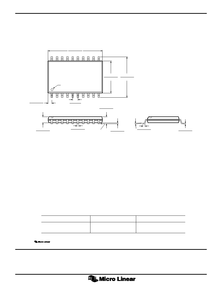
PHYSICAL DIMENSIONS
inches (millimeters)
SEATING PLANE
0.240 - 0.260
(6.09 - 6.61)
PIN 1 ID
0.295 - 0.325
(7.49 - 8.26)
1.010 - 1.035
(25.65 - 26.29)
0.016 - 0.022
(0.40 - 0.56)
0.100 BSC
(2.54 BSC)
0.008 - 0.012
(0.20 - 0.31)
0.015 MIN
(0.38 MIN)
20
0∫ - 15∫
1
0.055 - 0.065
(1.40 - 1.65)
0.170 MAX
(4.32 MAX)
0.125 MIN
(3.18 MIN)
0.060 MIN
(1.52 MIN)
(4 PLACES)
Package: P20
20-Pin PDIP
ML4830
15
Micro Linear reserves the right to make changes to any product herein to improve reliability, function or
design. Micro Linear does not assume any liability arising out of the application or use of any product
described herein, neither does it convey any license under its patent right nor the rights of others. The
circuits contained in this data sheet are offered as possible applications only. Micro Linear makes no
warranties or representations as to whether the illustrated circuits infringe any intellectual property rights of
others, and will accept no responsibility or liability for use of any application herein. The customer is urged
to consult with appropriate legal counsel before deciding on a particular application.
DS4830-01
2092 Concourse Drive
San Jose, CA 95131
Tel: 408/433-5200
Fax: 408/432-0295
ORDERING INFORMATION
PART NUMBER
TEMPERATURE RANGE
PACKAGE
ML4830CP (EOL)
0∞C to 85∞C
Molded PDIP (P20)
ML4830CS (Obsolete)
0∞C to 85∞C
Molded SOIC (S20)
© Micro Linear 1997
is a registered trademark of Micro Linear Corporation
Products described in this document may be covered by one or more of the following patents, U.S.: 4,897,611; 4,964,026; 5,027,116; 5,281,862; 5,283,483; 5,418,502; 5,508,570; 5,510,727; 5,523,940; 5,546,017;
5,559,470; 5,565,761; 5,592,128; 5,594,376; Japan: 2598946. Other patents are pending.
SEATING PLANE
0.291 - 0.301
(7.39 - 7.65)
PIN 1 ID
0.398 - 0.412
(10.11 - 10.47)
0.498 - 0.512
(12.65 - 13.00)
0.012 - 0.020
(0.30 - 0.51)
0.050 BSC
(1.27 BSC)
0.022 - 0.042
(0.56 - 1.07)
0.095 - 0.107
(2.41 - 2.72)
0.005 - 0.013
(0.13 - 0.33)
0.090 - 0.094
(2.28 - 2.39)
20
0.007 - 0.015
(0.18 - 0.38)
0∫ - 8∫
1
0.024 - 0.034
(0.61 - 0.86)
(4 PLACES)
Package: S20
20-Pin SOIC
PHYSICAL DIMENSIONS
inches (millimeters)