 | –≠–ª–µ–∫—Ç—Ä–æ–Ω–Ω—ã–π –∫–æ–º–ø–æ–Ω–µ–Ω—Ç: ML4863CS | –°–∫–∞—á–∞—Ç—å:  PDF PDF  ZIP ZIP |

July 2000
ML4863
*
High Efficiency Flyback Controller
1
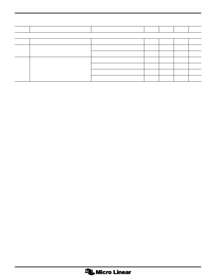
BLOCK DIAGRAM
GENERAL DESCRIPTION
The ML4863 is a flyback controller designed for use in
multi-cell battery powered systems such as PDAs and
notebook computers. The flyback topology is ideal for
systems where the battery voltage can be either above or
below the output voltage, and where multiple output
voltages are required.
The ML4863 uses the output voltage as the feedback
control signal to the current mode variable frequency
flyback controller. In addition, a synchronous rectifier
control output is supplied to provide the highest possible
conversion efficiency (greater than 85% efficiency over a
1mA to 1A load range).
The ML4863 has been designed to operate with a
minimum number of external components to optimize
space and cost.
*Some Packages Are Obsolete
FEATURES
s
Variable frequency current mode control and
synchronous rectification for high efficiency
s
Minimum external components
s
Guaranteed start-up and operation over a wide input
voltage range (3.15V to 15V)
s
High frequency operation (>200kHz) minimizes the
size of the magnetics
s
Flyback topology allows multiple outputs in addition to
the regulated 5V
s
Built-in overvoltage and current limit protection
SWITCHING
CONTROL
BLANKING
CROSS-CONDUCTION
PROTECTION
VFB
I
4.5V
LDO
RECTIFIER
COMPARATOR
CURRENT
COMPARATOR
Rgm
18mV
≠
+
VREF
3
SHDN
5
VCC
8
GND
6
OUT 1
7
OUT 2
2
SENSE
1
VIN
VFB
VCC
4
VFB
BIAS & UVLO
+
≠
COMP
≠
+
COMP
18mV
VCC
VCC
A2
A1
FEATURING
Extended Commercial Temperature Range
-20∞C to 70∞C
for Portable Handheld Equipment

ML4863
2
PIN CONFIGURATION
PIN
NAME
FUNCTION
1
V
IN
Battery input voltage
2
SENSE
Secondary side current sense
3
SHDN
Pulling this pin high initiates a
shutdown mode to minimize battery
drain
4
V
FB
Feedback input from transformer
secondary, and supply voltage when
V
OUT
> 4.5V
PIN DESCRIPTION
PIN
NAME
FUNCTION
5
V
CC
Internal power supply node for
connection of a bypass capacitor
6
OUT 1
Flyback primary switch MOSFET driver
output
7
OUT 2
Flyback synchronous rectifier MOSFET
driver output
8
GND
Analog signal ground
ML4863
8-Pin SOIC (S08)
1
2
3
4
8
7
6
5
VIN
SENSE
SHDN
VFB
GND
OUT 2
OUT 1
VCC
TOP VIEW

ML4863
3
ABSOLUTE MAXIMUM RATINGS
Absolute maximum ratings are those values beyond which
the device could be permanently damaged. Absolute
maximum ratings are stress ratings only and functional
device operation is not implied.
V
IN .................................................................
GND ≠ 0.3V to 18V
Voltage on any other pin
...........................
GND ≠ 0.3V to 7V
Source or Sink Current (OUT1 & OUT2) ...................... 1A
Junction Temperature .............................................. 150∫C
Storage Temperature Range...................... ≠65∫C to 150∫C
ELECTRICAL CHARACTERISTICS
Unless otherwise specified, V
IN
= 12V, T
A
= Operating Temperature Range (Note 1)
SYMBOL
PARAMETER
CONDITIONS
MIN
TYP
MAX
UNITS
OSCILLATOR
t
ON
ON Time
C Suffix
2.1
2.5
2.8
µs
E/I Suffix
2.1
2.5
2.95
µs
Minimum Off Time
V
FB
= 0V
450
650
850
ns
V
FB
REGULATION
Total Variation
Line, Load, & Temp
4.85
5
5.15
V
OUTPUT DRIVERS
OUT1 Rise Time
C
LOAD
= 3nF, 20% to 90% of V
CC
60
70
ns
OUT1 Fall Time
C
LOAD
= 3nF, 90% to 20% of V
CC
60
70
ns
OUT2 Rise Time
C
LOAD
= 3nF, 20% to 90% of V
CC
60
70
ns
OUT2 Fall Time
Continuous Mode, C
LOAD
= 3nF,
90% to 20% of V
CC
60
70
ns
Discontinuous Mode, C
LOAD
= 3nF,
90% to 20% of V
CC
125
150
ns
SHDN
Input High Voltage
2.0
V
Input Low Voltage
0.8
V
Input Bias Current
SHDN = 5V
5
10
µA
SENSE
SENSE Threshold ≠ Full Load
V
IN
= 5V, V
FB
= V
FB (No Load)
≠ 100mV
130
150
160
mV
SENSE Threshold ≠ Short Circuit
V
FB
= 0V
235
mV
CIRCUIT PROTECTION
Undervoltage Lockout Start-up Threshold
3.0
3.15
V
Undervoltage Lockout Hysteresis
0.5
0.6
V
Lead Temperature (Soldering 10 Sec.) ..................... 260∫C
Thermal Resistance (
q
JA
) .................................... 160∫C/W
OPERATING CONDITIONS
Temperature Range
ML4863CS ................................................. 0∫C to 70∫C
ML4863ES ............................................. ≠20∫C to 70∫C
ML4863IS .............................................. ≠40∫C to 85∫C
V
IN
Operating Range ................................... 3.15V to 15V
ML4863
4
ELECTRICAL CHARACTERISTICS
(Continued)
SYMBOL
PARAMETER
CONDITIONS
MIN
TYP
MAX
UNITS
SUPPLY
I
FB
V
FB
Quiescent Current
100
150
µA
I
IN
V
IN
Shutdown Current
SHDN = 5V
20
25
µA
SHDN = 5V, V
IN
< 6V
5
10
µA
V
CC
V
CC
Output Voltage
V
FB
= 0V, V
IN
= 15V, C
VCC
= 0.1µF
4.5
5.5
V
V
FB
= 0V, V
IN
= 6V, C
VCC
= 0.1µF
4.0
5.0
V
V
FB
= 0V, V
IN
= 3.15V, C
VCC
= 0.1µF
2.8
V
V
FB
= 5V
4.5
5
5.15
V
Note 1:
Limits are guaranteed by 100% testing, sampling, or correlation with worst case test conditions.
ML4863
5
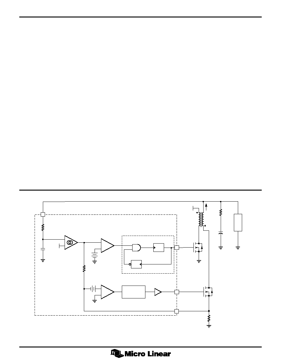
FUNCTIONAL DESCRIPTION
The ML4863 utilizes a flyback topology with constant on-
time control. The circuit determines the length of the off-
time by waiting for the inductor current to drop to a level
determined by the feedback voltage (V
FB
). Consequently,
the current programming is somewhat unconventional
because the valley of the current ripple is programmed
instead of the peak. The controller automatically enters
burst mode when the programmed current falls below
zero. Constant on-time control therefore features a
transition into and out of burst mode which does not
require additional control circuitry.
The control circuit is made up of four distinctive blocks;
the constant on-time oscillator, the current programming
comparator, the feedback transconductance amplifier, and
the synchronous rectifier controller. A simplified circuit
diagram is shown in Figure 1.
OSCILLATOR & COMPARATOR
The oscillator has a constant on-time and a minimum off-
time. The off-time is extended as long as the output of the
current programming comparator is low. Note that in
constant on-time control, a discharge (off-time) cycle is
needed for the inductor current to be sensed. The
minimum off-time is required to account for the finite
circuit delays in sensing the inductor output current.
TRANSCONDUCTANCE AMPLIFIER
The feedback transconductance amplifier generates a
current from the voltage difference between the output
and the reference. This current produces a voltage across
R
gm
that adds to the negative voltage on the current sense
resistor, R
SENSE
. When the current level in the inductor
drops low enough to cause the voltage at the non-inverting
input of the current programming comparator to go
positive, the comparator trips and the converter starts a
new on-cycle. The current programming comparator
controls the length of the off-time by waiting until the
current in the secondary decreases to the value specified
by the feedback transconductance amplifier.
In this way, the feedback transconductance amplifier`s
output current steers the current level in the inductor.
When the output voltage drops due to a load increase, it
will increase the output current of the feedback amplifier
and generate a larger voltage across R
gm
which in turn
raises the secondary current trip level. However, when the
output voltage is too high, the feedback amplifier's output
current will eventually become negative. Because the
output current of the inductor can never go negative by
virtue of the diode, the non-inverting input of the
comparator will also stay negative. This causes the
converter to stop operation until the output voltage drops
enough to increase the output current of the feedback
transconductance amplifier above zero.
Figure 1. Schematic of the ML4863 Controller and Power Stage
LO
AD
RP
CP
FEEDBACK
TRANSCONDUCTANCE
AMPLIFIER
Rgm
CURRENT
PROGRAMMING
COMPARATOR
ONE SHOT
t
ON
2.5µs
ONE SHOT
CONSTANT ON-TIME
MINIMUM OFF-TIME
OSCILLATOR
VIN
L
P
1:1
C
R
ESR
VOUT
RSENSE
BLANKING
A2
ML4863
RECTIFIER
COMPARATOR
IS
SENSE
OUT 2
OUT 1
≠
+
COMP
+
≠
COMP
+
≠
VREF
VFB
t
OFF
500ns
4
7
6
2