
GENERAL DESCRIPTION
The ML4871 is a continuous conduction boost regulator
designed for DC to DC conversion in multiple cell battery
powered systems. Continuous conduction allows the
regulator to maximize output current for a given inductor.
The maximum switching frequency can exceed 200kHz,
allowing the use of small, low cost inductors. The ML4871
is capable of start-up with input voltages as low as 1.8V
and is available in 5V and 3.3V output versions with an
output voltage accuracy of ±3%.
An integrated synchronous rectifier eliminates the need for
an external Schottky diode and provides a lower forward
voltage drop, resulting in higher conversion efficiency. In
addition, low quiescent battery current and variable
frequency operation result in high efficiency even at light
loads. The ML4871 requires only one inductor and two
capacitors to build a very small regulator circuit capable
of achieving conversion efficiencies approaching 90%.
The circuit also contains a RESET output which goes low
when the DETECT input drops below 1.25V.
BLOCK DIAGRAM
July 2000
ML4871
High Current Boost Regulator
1
FEATURES
s
Guaranteed full load start-up and operation
at 1.8V Input
s
Continuous conduction mode for high output current
s
Very low supply current (20µA output referenced) for
Micropower operation
s
Pulse Frequency Modulation and Internal Synchronous
Rectification for high efficiency
s
Maximum switching frequency > 200kHz
s
Minimum external components
s
Low ON resistance internal switching FETs
s
5V and 3.3V output versions
VL2
5
VOUT
6
+
≠
VIN
2
1.25V
START-UP
3
GND
VL1
1
DETECT
4
SYNCHRONOUS
RECTIFIER
CONTROL
BOOST
CONTROL
+
≠
+
≠
8
PWR GND
RESET
VREF
+
≠
COMP
7
FEATURING
Extended Commercial Temperature Range
-20∞C to 70∞C
for Portable Handheld Equipment
2
ML4871
PIN CONFIGURATION
PIN DESCRIPTION
NO.
NAME
FUNCTION
1
V
L1
Boost inductor connection
2
V
IN
Battery input voltage
3
GND
Ground
4
DETECT
Pulling this pin below 1.25V causes
the RESET pin to go low
NO.
NAME
FUNCTION
5
V
OUT
Boost regulator output
6
V
L2
Boost inductor connection
7
RESET
Output goes low when DETECT goes
below 1.25V
8
PWR GND Return for the NMOS output transistor
ML4871
8-Pin SOIC (S08)
1
2
3
4
8
7
6
5
VL1
VIN
GND
DETECT
PWR GND
RESET
VL2
VOUT
TOP VIEW
3
ML4871
ABSOLUTE MAXIMUM RATINGS
Absolute maximum ratings are those values beyond which
the device could be permanently damaged. Absolute
maximum ratings are stress ratings only and functional
device operation is not implied.
V
OUT
........................................................................... 7V
Voltage on Any Other Pin .... GND ≠ 0.3V to V
OUT
+ 0.3V
Peak Switch Current (I
PEAK
) .......................................... 2A
Average Switch Current (I
AVG
) ..................................... 1A
Junction Temperature .............................................. 150∫C
Storage Temperature Range...................... ≠65∫C to 150∫C
Lead Temperature (Soldering 10 sec) ....................... 260∫C
Thermal Resistance (
q
JA
) .................................... 160∫C/W
OPERATING CONDITIONS
Temperature Range
ML4871CS-X ............................................. 0∫C to 70∫C
ML4871ES-X .......................................... ≠20∫C to 70∫C
V
IN
Operating Range
ML4871CS-X ................................ 1.8V to V
OUT
≠ 0.2V
ML4871ES-X ................................. 2.0V to V
OUT
≠ 0.2V
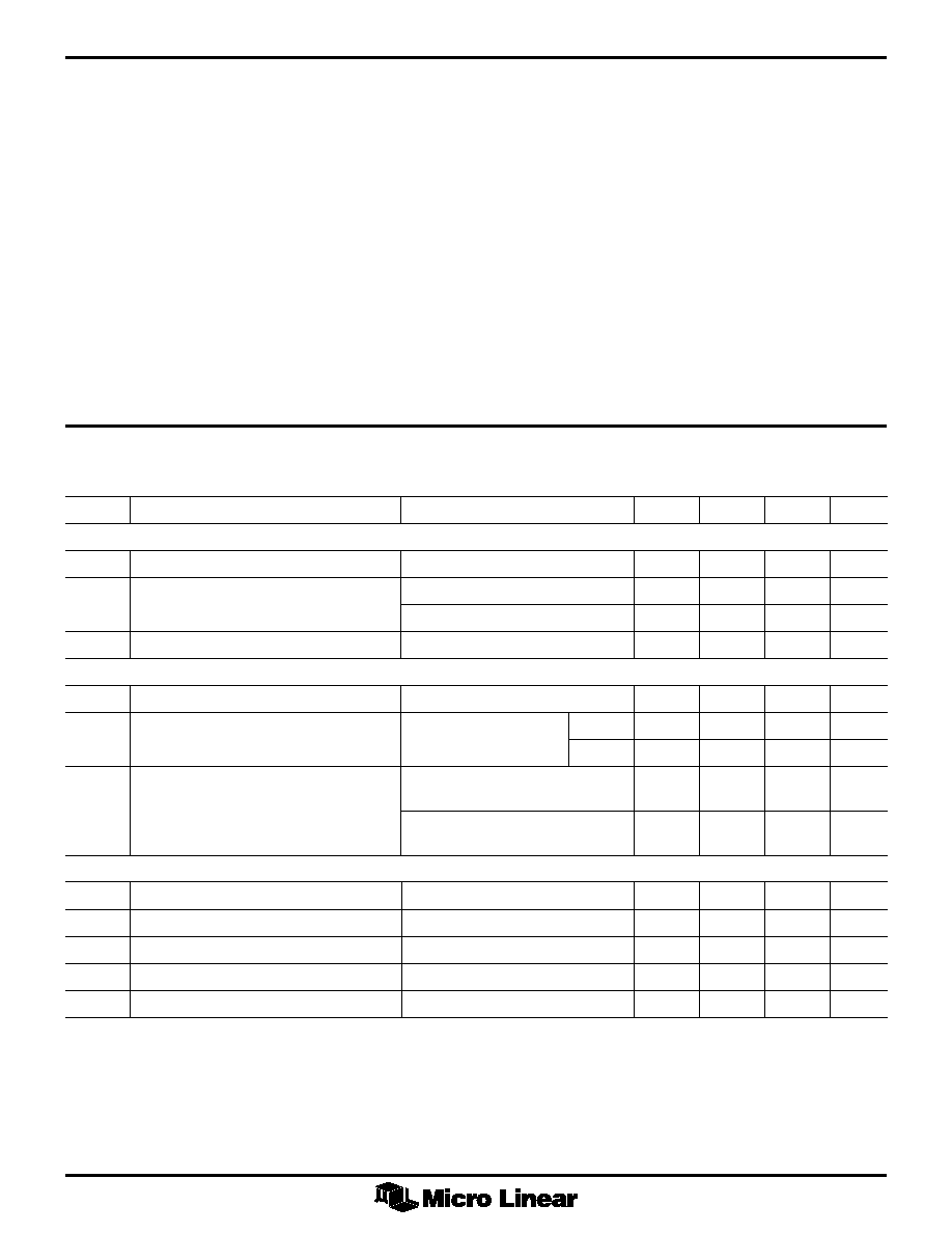
ELECTRICAL CHARACTERISTICS
Unless otherwise specified, V
IN
= Operating Voltage Range, T
A
= Operating Temperature Range (Note 1).
SYMBOL
PARAMETER
CONDITIONS
MIN
TYP
MAX
UNITS
SUPPLY
I
IN
V
IN
Current
V
IN
= V
OUT
≠ 0.2V
2
5
µA
I
OUT(Q)
V
OUT
Quiescent Current
DETECT = V
IN
30
40
µA
DETECT = 0V
25
35
µA
I
L(Q)
V
L
Quiescent Current
1
µA
PFM REGULATOR
I
L
Peak Current
1.2
1.4
1.7
A
V
OUT
Output Voltage
I
L(PEAK)
= 0
-3 Suffix
3.30
3.35
3.40
V
-5 Suffix
4.95
5.05
5.15
V
Load Regulation
See Figure 1, -3 Suffix
3.20
3.25
3.40
V
V
IN
= 2.4V, I
OUT
£ 400mA
See Figure 1, -5 Suffix
4.85
4.95
5.15
V
V
IN
= 2.4V, I
OUT
£ 220mA
RESET COMPARATOR
DETECT Threshold
1.18
1.25
1.28
V
DETECT Hysteresis
25
35
45
mV
DETECT Bias Current
≠100
100
nA
RESET Output High Voltage
I
RESET
= ≠200µA
V
OUT
≠ 0.2
V
RESET Output Low Voltage
I
RESET
= 500µA
0.2
V
Note 1:
Limits are guaranteed by 100% testing, sampling, or correlation with worst case test conditions.
4
ML4871
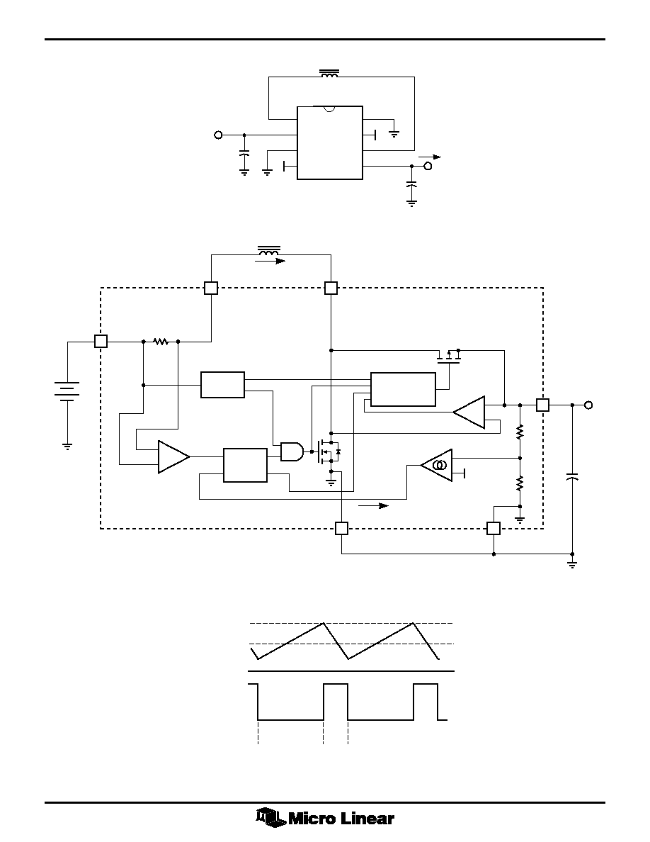
Figure 1. Application Test Circuit.
Figure 3. Inductor Current and Voltage Waveforms.
Figure 2. PFM Regulator Block Diagram.
ML4871
IOUT
200µF
100µF
VIN
20µH
(Sumida CD75)
VL1
VIN
GND
DETECT
PWR GND
RESET
VL2
VOUT
Q1 ON
Q2 OFF
Q1 OFF
Q2 ON
IL
VL2
IL(MAX)
ISET
VOUT
0
0
VL2
5
VOUT
6
+
≠
VIN
IL
2
1.25V
START-UP
3
GND
VL1
1
SYNCHRONOUS
RECTIFIER
CONTROL
BOOST
CONTROL
+
≠
+
≠
8
PWR GND
A1
A2
A3
Q1
Q2
VOUT
RSENSE
ISET
5
ML4871
FUNCTIONAL DESCRIPTION
The ML4871 combines a unique form of current mode
control with a synchronous rectifier to create a boost
converter that can deliver high currents while maintaining
high efficiency. Current mode control allows the use of a
very small, high frequency inductor and output capacitor.
Synchronous rectification replaces the conventional
external Schottky diode with an on-chip PMOS FET to
reduce losses and eliminate an external component. Also
included on-chip are an NMOS switch and current sense
resistor, further reducing the number of external
components, which makes the ML4871 very easy to use.
REGULATOR OPERATION
The ML4871 is a variable frequency, current mode
switching regulator. Its unique control scheme converts
efficiently over more than three decades of load current.
A block diagram of the boost converter is shown in Figure 2.
Error amp A3 converts deviations in the desired output
voltage to a small current, I
SET
. The inductor current is
measured through a 50m
W resistor which is amplified by
A1. The boost control block matches the average inductor
current to a multiple of the I
SET
current by switching Q1
on and off. The peak inductor current is limited by the
controller to about 1.5A.
At light loads, I
SET
will momentarily reach zero after an
inductor discharge cycle , causing Q1 to stop switching.
Depending on the load, this idle time can extend to tenths
of seconds. While the circuit is not switching, only 20µA
of supply current is drawn from the output. This allows the
part to remain efficient even when the load current drops
below 200µA.
Amplifier A2 and the PMOS transistor Q2 work together to
form a low drop diode. When transistor Q1 turns off, the
current flowing in the inductor causes pin 6 to go high. As
the voltage on V
L2
rises above V
OUT
, amplifier A2 allows
the PMOS transistor Q2 to turn on. In discontinuous
operation, (where I
L
always returns to zero), A2 uses the
resistive drop across the PMOS switch Q2 to sense zero
inductor current and turns the PMOS switch off. In
continuous operation, the PMOS turn off is independent of
A2, and is determined by the boost control circuitry.
Typical inductor current and voltage waveforms are shown
in Figure 3.
RESET COMPARATOR
An additional comparator is provided to detect low V
IN
,
low V
OUT
, or any other error condition that the user may
want to sense. The inverting input of the comparator is
connected to the 1.25V reference, and the non-inverting
input is connected to the DETECT pin. The output of this
comparator is connected to the RESET pin of the device
and can swing from V
OUT
to ground.
DESIGN CONSIDERATIONS
OUTPUT CURRENT CAPABILITY
The maximum current available at the output of the
regulator is related to the maximum inductor current by
the ratio of the input to output voltage and the full load
efficiency. The maximum inductor current is
approximately 1.25A and the full load efficiency may be
as low as 70%. The maximum output current can be
determined by using the typical performance curves
shown in Figures 4 and 5, or by calculation using the
following equation:
I
V
V
A
OUT MAX
IN MIN
OUT
(
)
(
)
.
.
=
125
0 7
(1)
INDUCTOR SELECTION
The ML4871 is able to operate over a wide range of
inductor values. A value of 10µH is a good choice, but any
value between 5µH and 33µH is acceptable. As the
inductor value is changed the control circuitry will
automatically adjust to keep the inductor current under
control. Choosing an inductance value of less than 10µH
will reduce the component's footprint, but the efficiency
and maximum output current may drop.
It is important to use an inductor that is rated to handle 1.5A
peak currents without saturating. Also look for an inductor
with low winding resistance. A good rule of thumb is to
allow 5 to 10m
W of resistance for each µH of inductance.
The final selection of the inductor will be based on trade-
offs between size, cost and efficiency. Inductor tolerance,
core and copper loss will vary with the type of inductor
selected and should be evaluated with a ML4871 under
worst case conditions to determine its suitability.
Several manufacturers supply standard inductance values
in surface mount packages:
Coilcraft
(847) 639-6400
Coiltronics
(561) 241-7876
Dale
(605) 665-9301
Sumida
(847) 956-0666