
March 1997
ML6401
*
8-Bit 20 MSPS A/D Converter
1
GENERAL DESCRIPTION
The ML6401 is a single-chip 8-bit 20 MSPS BiCMOS Video
A/D Converter IC, incorporating a differential input track
and hold, clock generation circuitry, and reference voltage.
The input track and hold consists of a low (4pF)
capacitance input and a fast settling operational amplifier.
The A/D conversion is accomplished through a pipeline
approach, reducing the number of required comparators
and latches. The non-over-lapping clocks required for this
architecture are all internally generated. Clock generation
circuitry requires only one 50% duty cycle clock input.
The use of error correction throughout the A/D converter
improves DNL. All bias voltages and currents required by
the A/D converter are internally generated. The digital
outputs are three-stateable.
FEATURES
s 5.0V
±
10% single supply operation
s Internal reference voltage
s Power dissipation less than 200mW typical
s Replaces TMC1175MC20 and AD775JR,
functionally compatible to Sony CXD1175AM/AP
s 16-pin reduced pin count packages
available: ML6401CS-3
s Low input capacitance track and hold: 4pF
s Onboard non-overlapping clock generation to
minimize external components
s Three-state outputs and no missing codes
s 150MHz input track and hold
BLOCK DIAGRAM/TYPICAL APPLICATION
*Some Packages Are End Of Life
DIGITAL
ERROR
CORRECTION
OE
D7
D6
D5
D4
D3
D2
D1
D0
VDD
D
VDD
A
VDD
A
VDD
A
VDD
D
GND
O
GND
D
GND
A
GND
A
CLK
5V
CLOCK GENERATOR
20MHz
SUB
DAC
AMP
SUB
DAC
AMP
ADC 3
ADC 2
ADC 1
150MHz
T & H
V
IN
+
V
IN
≠
INTERNAL
REFERENCES
1.5V
1.0V
1k
1k
75
VIDEO
INPUT
+
+
10
µ
F
47
µ
F
0.1
µ
F
VIN
-BIAS
VREF
OUT
VREF
IN
2
ML6401
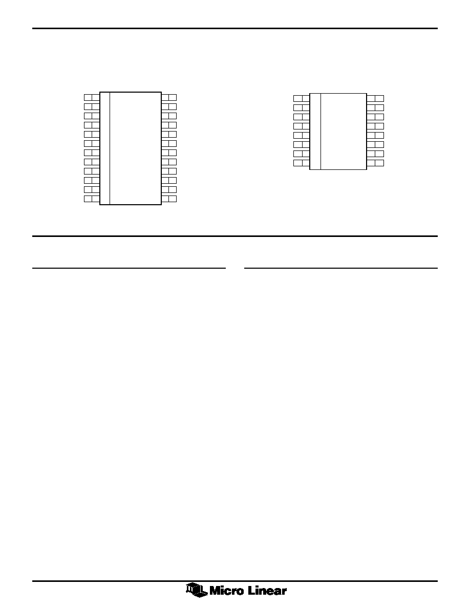
PIN CONFIGURATION
ML6401-1
24-Pin SOIC (S24W)
ML6401-3
16-Pin SOIC (S16N)
GND
D
V
IN
≠
V
IN≠BIAS
GNDA
GNDA
V
IN
+
VDD
A
VREF
IN
VREF
OUT
VDD
A
VDD
A
VDD
D
OE
GND
O
D0
D1
D2
D3
D4
D5
D6
D7
VDD
O
CLK
24
23
22
21
20
19
18
17
16
15
14
13
1
2
3
4
5
6
7
8
9
10
11
12
TOP VIEW
OE
GND
D
GND
A
V
IN
+
VDD
A
VDD
D
CLK
VDD
D
D0
D1
D2
D3
D4
D5
D6
D7
16
15
14
13
12
11
10
9
1
2
3
4
5
6
7
8
TOP VIEW
PIN
NAME
DESCRIPTION
1
(16)
OE
Output Enable. A logic low signal
on this pin enables the outputs.
2
GND
O
Output ground pin.
3
(1)
D0
D0 (LSB) output signal (TTL
compatible).
4
(2)
D1
D1 output signal (TTL compatible).
5
(3)
D2
D2 output signal (TTL compatible).
6
(4)
D3
D3 output signal (TTL compatible).
7
(5)
D4
D4 output signal (TTL compatible).
8
(6)
D5
D5 output signal (TTL compatible).
9
(7)
D6
D6 output signal (TTL compatible).
10 (8)
D7
D7 (MSB) output signal (TTL
compatible).
11
VDD
O
Output supply pin.
12 (10)
CLK
Clock input pin.
PIN
NAME
DESCRIPTION
13 (9,11) VDD
D
Digital supply pin.
14 (12)
VDD
A
Analog supply pin.
15 (12)
VDD
A
Analog supply pin.
16
VREF
OUT
Full scale reference output.
Connect to pin 17 for self bias.
(VRTS on 1175) (ML401-1 only)
17
VREF
IN
Full scale reference input.
Connect to pin 16 for self bias.
(VRT on 1175) (ML401-1 only)
18 (12)
VDD
A
Analog supply pin.
19 (13)
V
IN
+
Input signal.
20 (14)
GND
A
Analog ground.
21 (14)
GND
A
Analog ground.
22
V
IN≠BIAS
Common mode bias output.
Connect to pin 23 for self bias.
(VRBS on 1175) (ML401-1 only)
23
V
IN
≠
Common mode bias input.
Connect to pin 22 for self bias.
Drive with the negative input if
differential input is being used.
(VRB on 1175)
(ML401-1 only)
24 (15)
GND
D
Digital Ground.
PIN DESCRIPTION
(Pin numbers in parentheses are for S16N package)

3
ML6401
ELECTRICAL CHARACTERISTICS
Unless otherwise specified, C
L
= 15pF, V
CC
= 5V
±
10%, T
A
= Operating Temperature Range (Note 1).
PARAMETER
CONDITIONS
MIN
TYP
MAX
UNITS
Resolution
8
Bits
Power Dissipation
200
325
mW
Transfer Function
DC Integral Linearity
f
CLk
= 15MSPS
±
0.8
±
1.25
LSB
DC Differential Linearity
f
CLk
= 15MSPS
±
0.6
±
1
LSB
AC Integral Linearity
V
IN
= 2V, 4.4MHz
±
2
LSB
Offset Voltage
V
IN
≠ = V
IN≠BIAS
, VREF
OUT
= VREF
IN
±
10
LSB
Gain Error
V
IN
≠ = V
IN≠BIAS
, VREF
OUT
= VREF
IN
±
2
±
5
LSB
Analog Signal Processing
Differential Gain
V
IN
= NTSC 40 IRE modulated ramp,
f
CLK
= 14.3 MSPS
1.8
%
Differential Phase
V
IN
= NTSC 40 IRE modulated ramp,
f
CLK
= 14.3 MSPS
0.9
degree
Signal to Noise Ratio
V
IN
= 2V, 1MHz, f
CLK
= 20MHz
48
dB
Distortion
0.18
%
Spurious Free Dynamic Range
58
dB
SIN and Distortion (SINAD)
47
dB
Effective Bits
7.4
bits
Analog Inputs
Input Voltage
Digital Output = 0,
V
IN
≠ = V
IN≠BIAS
, VREF
OUT
= VREF
IN
0.5
V
Digital Output = 255,
V
IN
≠ = V
IN≠BIAS
, VREF
OUT
= VREF
IN
2.5
V
Input Current
f
CLK
= 20MHz
±
20
±
30
µ
A
Input Capacitance
V
IN
= 2V
4.0
pF
Analog Input Bandwidth
150
MHz
Reference Outputs
V
IN≠BIAS
1.45
1.5
1.55
V
VREF
OUT
IREF
OUT
= 50
µ
A
0.97
1.0
1.03
V
V
RIN
±
5
µ
A
ABSOLUTE MAXIMUM RATINGS
Absolute maximum ratings are those values beyond which
the device could be permanently damaged. Absolute
maximum ratings are stress ratings only and functional
device operation is not implied.
Supply Current (I
CC
) ............................................... 55mA
Peak Driver Output Current ...............................
±
500mA
Analog Inputs ................................................... ≠0.3 to 7V
Junction Temperature ............................................. 150
∞
C
Storage Temperature Range ..................... ≠65
∞
C to 150
∞
C
Lead Temperature (soldering, 10 sec) ..................... 150
∞
C
Thermal Resistance (
JA
)
Plastic DIP ....................................................... 80
∞
C/W
Plastic SOIC ................................................... 110
∞
C/W
OPERATING CONDITIONS
Temperature Range ....................................... 0
∞
C to 70
∞
C
T
PWH(min)
= T
PWL(min)
............................................... 25ns

4
ML6401
ELECTRICAL CHARACTERISTICS
(Continued)
PARAMETER
CONDITIONS
MIN
TYP
MAX
UNITS
Switching Characteristics
Maximum CLK Input Frequency
20
25
MHz
Clock Duty Cycle
CLK = 13.5MHz
40
60
%
t
PWH
CLK
20MHz
25
ns
t
PWL
CLK
20MHz
25
ns
Analog To Digital Converter Inputs -- CLK
Low Level Input Voltage
V
IL
0
0.8
V
High Level Input Voltage
V
IH
2.4
VDD
D
V
Low Level Input Current
V
IL
= 0.1V
≠5
+5
µ
A
High Level Input Current
V
IH
= VDD
D
≠ 0.1V
≠5
+5
µ
A
Input Capacitance
4.0
pF
Timing -- Digital Outputs (C
L
= 15pF, I
OL
= 2mA, R
L
= 2k
, f
CLK
= 20MHz)
Sampling Delay
t
DS
5
ns
Output Hold Time
t
HO
4
12
10
ns
Output Delay Time
t
DO
5
18
30
ns
Three-State Delay Time -- Output Enable
10
25
ns
Three-State Delay Time -- Output Disable
10
20
ns
Analog To Digital Converter Outputs -- Digital
Low Level Output Voltage
I
OL
= 2mA
0
0.6
V
High Level Output Voltage
I
OH
= 2mA
2.4
VCC
O
V
Output Current in Three-State Mode
≠20
+20
µ
A
Supplies
Analog, Digital & Output Supply Voltage
4.5
5.5
V
Analog Supply Current
Static
26
34
mA
Digital Supply Current
f
CLK
= 20MHz
10
15
mA
Output Supply Current
f
CLK
= 20MHz, C
L
= 0pF
4
10
mA
(V
IN
+) ≠ (V
IN
≠)
CLK
D0 TO D7
SAMPLE
OUT
N
N+1
N+2
N+3
N+4
N≠3
N≠2
N≠1
N
N+1
t
DS
t
PWH
t
PWL
t
HO
t
DO
TIMING DIAGRAM
Note 1: Limits are guaranteed by 100% testing, sampling, or correlation with worst-case test conditions.

5
ML6401
FUNCTIONAL DESCRIPTION
INTRODUCTION
The Micro Linear ML6401 is a single-chip video A/D
converter IC which is intended for analog to digital
conversion of 2Vp-p signals at rates up to 20MSPS.
Incorporating both bias and clock generation, it forms a
complete solution for data conversion. The operating
power dissipation is typically less than 200mW. The IC is
designed to offer low power dissipation and a high level
of integration resulting in an optimized solution. The IC
consists of an input track and hold, a three stage pipelined
A/D converter, digital error correction circuitry, internal
dual non-overlapping clock generator, and internal
voltage reference.
INPUT TRACK AND HOLD
The input track and hold consists of a differential
capacitor feedback amplifier. The input capacitance,
including pin protection and transmission gate, is 4pF.
The input to the track and hold can be driven differentially,
or single-ended. Single-ended operation uses an internal
or external reference to bias the negative input. The full
scale range can be set externally, or supplied from an
internal source. The track and hold samples the input
signal during the positive half cycle of the input clock,
and holds the last value of V
IN
during the negative half
cycle of the input clock. The settling time of the amplifier
is less than 20ns.
8
7
6
1
2
3
4
5
6
7
8
9
10
FREQUENCY
EFB
Typical Effective Bits versus Input Signal Frequency.
A/D CONVERTER
The A/D conversion is performed via a three stage
pipelined architecture. The first two stages quantize their
input signal to three bits, then subtract the result from the
input and amplify the difference by a factor of four. This
creates a residue signal which spans the full scale range of
the following converter. The subtraction and amplification
is performed via a differential capacitor feedback
amplifier, similar to the input track and hold. The third
stage quantizes the signal to four bits. One bit from each
of the last two stages is used for error correction.
The first stage A/D performs the conversion at the end of
the track and hold period, approximately one-half cycle
after the input was sampled. The second stage A/D
performs the conversion one half cycle later, after the
subtraction/amplification of the first stage has settled. The
third stage A/D performs the conversion after another one-
half cycle delay, when the second stage has settled. Error
correction is then performed, and, one clock cycle later,
data is transferred to the output latch. This permits the
data to be read 3 clocks after the sample was taken.
This technique results in lower input capacitance, lower
harmonic distortion, and higher signal to noise ratios than
the classical two step parallel technique, providing a
greater number of effective bits.
CLOCK GENERATION
The ML6401 typically requires an input clock that if
running at 20MHz would have a low time of 25ns, and a
high time of 25ns. This input is applied to a clock
generation circuit which creates the two non-overlapping
clock signals required by the feedback amplifiers.
Pipeline delay is the number of clock cycles between
conversion initiation and the associated output data being
made available. New output data is provided every clock
cycle.