
BLOCK DIAGRAM
1
August 2000
PRELIMINARY
ML6516244
*
16-Bit Buffer/Line Driver with 3-State Outputs
GENERAL DESCRIPTION
The ML6516244 is a BiCMOS, 16-bit buffer/line driver
with 3-state outputs. This device was specifically designed
for high speed bus applications. Its 16 channels support
propagation delay of 2.5ns maximum, and fast output
enable and disable times of 7.0ns or less to minimize
datapath delay.
This device is designed to minimize undershoot,
overshoot, and ground bounce to decrease noise delays.
These transceivers implement a unique digital and analog
implementation to eliminate the delays and noise inherent
in traditional digital designs. The device offers a new
method for quickly charging up a bus load capacitor to
minimize bus settling times, or FastBusTM Charge. FastBus
Charge is a transition current, (specified as I
DYNAMIC
) that
injects between 60 to 200mA (depending on output load)
of current during the rise time and fall time. This current is
used to reduce the amount of time it takes to charge up a
heavily-capacitive loaded bus, effectively reducing the
bus settling times, and improving data/clock margins in
tight timing budgets.
Micro Linear's solution is intended for applications for
critical bus timing designs that include minimizing device
propagation delay, bus settling time, and time delays due
to noise. Applications include; high speed memory arrays,
bus or backplane isolation, bus to bus bridging, and sub-
2.5ns propagation delay schemes.
The ML6516244 follows the pinout and functionality of
the industry standard 3.3V-logic families.
FEATURES
s
Low propagation delays -- 2.5ns maximum for 3.3V
2.25ns maximum for 5.0V
s
Fast output enable/disable times of 5.0ns maximum
s
FastBus Charge current to minimize the bus settling
time during active capacitive loading
s
3.0 to 3.6V and 4.5 to 5.5V V
CC
supply operation;
LV-TTL compatible input and output levels with 3-state
capability
s
Industry standard pinout compatible to FCT, ALV, LCX,
LVT, and other low voltage logic families
s
ESD protection exceeds 2000V
s
Full output swing for increased noise margin
s
Undershoot and overshoot protection to 400mV
typically
s
Low ground bounce design
V
CC
GND
1 of 4
A0
OE
B1
B0
A1
B2
A2
B3
A3
* This part is End of Life as of August 1, 2000.
ML6516244
2
PIN CONFIGURATION
FUNCTION TABLE
(Each 4-bit section)
INPUTS
OUTPUTS
OE
1Ai, 2Ai, 3Ai, 4Ai
1Bi, 2Bi, 3Bi, 4Bi
L
H
H
L
L
L
H
X
Z
L = Logic Low, H = Logic High, X = Don't Care, Z = High Impedance
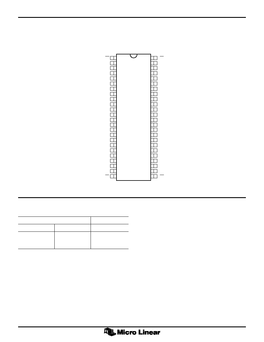
TOP VIEW
1
2
3
4
5
6
7
8
9
10
20
19
18
17
16
15
14
13
12
11
1
2
3
4
5
6
7
8
9
10
11
12
13
14
15
16
17
18
19
20
21
22
23
24
2OE
1A0
1A1
GND
1A2
1A3
V
CC
2A0
2A1
GND
2A2
2A3
3A0
3A1
GND
3A2
3A3
V
CC
4A0
4A1
GND
4A2
4A3
3OE
1OE
1B0
1B1
GND
1B2
1B3
V
CC
2B0
2B1
GND
2B2
2B3
3B0
3B1
GND
3B2
3B3
V
CC
4B0
4B1
GND
4B2
4B3
4OE
48
47
46
45
44
43
42
41
40
39
38
37
36
35
34
33
32
31
30
29
28
27
26
25
ML6516244
48-Pin SSOP (R48)
48-Pin TSSOP (T48)

ML6516244
3
PIN DESCRIPTION
PIN
NAME
FUNCTION
1
1OE
Output Enable
2
1B0
Data Output
3
1B1
Data Output
4
GND
Signal Ground
5
1B2
Data Output
6
1B3
Data Output
7
V
CC
3.3V or 5.0V Supply
8
2B0
Data Output
9
2B1
Data Output
10
GND
Signal Ground
11
2B2
Data Output
12
2B3
Data Output
13
3B0
Data Output
14
3B1
Data Output
15
GND
Signal Ground
16
3B2
Data Output
17
3B3
Data Output
18
V
CC
3.3V or 5.0V Supply
19
4B0
Data Output
20
4B1
Data Output
21
GND
Signal Ground
22
4B2
Data Output
23
4B3
Data Output
24
4OE
Output Enable
PIN
NAME
FUNCTION
25
3OE
Output Enable
26
4A3
Data Input
27
4A2
Data Input
28
GND
Signal Ground
29
4A1
Data Input
30
4A0
Data Input
31
V
CC
3.3V or 5.0V Supply
32
3A3
Data Input
33
3A2
Data Input
34
GND
Signal Ground
35
3A1
Data Input
36
3A0
Data Input
37
2A3
Data Input
38
2A2
Data Input
39
GND
Signal Ground
40
2A1
Data Input
41
2A0
Data Input
42
V
CC
3.3V or 5.0V Supply
43
1A3
Data Input
44
1A2
Data Input
45
GND
Signal Ground
46
1A1
Data Input
47
1A0
Data Input
48
2OE
Output Enable

ML6516244
4
ABSOLUTE MAXIMUM RATINGS
Absolute maximum ratings are those values beyond which
the device could be permanently damaged. Absolute
maximum ratings are stress ratings only and functional
device operation is not implied.
V
CC
............................................................................. 7V
DC Input Voltage .............................. ≠0.3V to V
CC
+ 0.3V
AC Input Voltage (PW < 20ns) ................................. ≠3.0V
DC Output Voltage ................................... ≠0.3V to 7VDC
Output Current, Source or Sink ............................. 180mA
Storage Temperature Range...................... ≠65įC to 150įC
Junction Temperature ............................................. 150įC
Lead Temperature (Soldering, 10sec) ...................... 150įC
Thermal Impedance (
q
JA
) ..................................... 76įC/W
OPERATING CONDITIONS
Temperature Range ........................................ 0įC to 70įC
V
IN
Operating Range ................................... 3.0V to 5.5V
ELECTRICAL CHARACTERISTICS ≠ 3.3V OPERATION
Unless otherwise specified, V
IN
= 3.3V, T
A
= Operating Temperature Range (Note 1).
SYMBOL
PARAMETER
CONDITIONS
MIN
TYP
MAX
UNITS
AC ELECTRICAL CHARACTERISTICS (C
LOAD
= 50pF)
t
PHL
, t
PLH
Propagation Delay
Ai to Bi
1.8
2.1
2.5
ns
t
OE
Output Enable Time
OE to Ai
7.0
ns
t
OD
Output Disable Time
OE to Ai
7.0
ns
T
OS
Output-to-Output Skew
500
ps
C
IN
Input Capacitance
5
pF
DC ELECTRICAL CHARACTERISTICS (C
LOAD
= 50pF, R
LOAD
= Open)
V
IH
Input High Voltage
Logic high
2.0
V
V
IL
Input Low Voltage
Logic low
0.8
V
I
IH
Input High Current
Per pin, V
IN
= 3V
300
mA
I
IL
Input Low Current
Per pin, V
IN
= 0V
300
mA
I
HI-Z
Three-State Output Current
V
CC
= 3.6V, 0 < V
IN
< V
CC
5
mA
V
IC
Input Clamp Voltage
V
CC
= 3.6V, I
IN
= 18mA
≠0.7
≠0.2
V
I
DYNAMIC
Dynamic Transition Current
Low to high transitions
80
mA
(FastBus Charge)
High to low transitions
80
mA
V
OH
Output High Voltage
V
CC
= 3.6V, I
OH
= ≠2mA
2.4
V
V
OL
Output LowVoltage
V
CC
= 3.6V, I
OL
= 2mA
0.6
V
I
CC
Quiescent Power Supply Current
V
CC
= 3.6V, f = 0Hz,
3
mA
inputs = V
CC
or 0V
Note 1: Limits are guaranteed by 100% testing, sampling, or correlation with worst-case test conditions.

ML6516244
5
Note 1: Limits are guaranteed by 100% testing, sampling, or correlation with worst-case test conditions.
ELECTRICAL CHARACTERISTICS ≠ 5V OPERATION
Unless otherwise specified, V
IN
= 5V, T
A
= Operating Temperature Range (Note 1).
SYMBOL
PARAMETER
CONDITIONS
MIN
TYP
MAX
UNITS
AC ELECTRICAL CHARACTERISTICS (C
LOAD
= 50pF)
t
PHL
, t
PLH
Propagation Delay
Ai to Bi
1.6
1.9
2.25
ns
t
OE
Output Enable Time
OE to Ai
7.0
ns
t
OD
Output Disable Time
OE to Ai/Bi
7.0
ns
T
OS
Output-to-Output Skew
500
ps
C
IN
Input Capacitance
5
pF
DC ELECTRICAL CHARACTERISTICS (C
LOAD
= 50pF, R
LOAD
= Open)
V
IH
Input High Voltage
Logic high
3.6
V
V
IL
Input Low Voltage
Logic low
0.8
V
I
IH
Input High Current
Per pin, V
IN
= 4.5V
300
mA
I
IL
Input Low Current
Per pin, V
IN
= 0V
300
mA
I
HI-Z
Three-State Output Current
V
CC
= 5.5V, 0 < V
IN
< V
CC
5
mA
V
IC
Input Clamp Voltage
V
CC
= 5.5V, I
IN
= 18mA
≠0.7
≠0.2
V
I
DYNAMIC
Dynamic Transition Current
Low to high transitions
120
mA
(FastBus Charge)
High to low transitions
120
mA
V
OH
Output High Voltage
V
CC
= 5.5V, I
OH
= ≠2mA
4.5
V
V
OL
Output Low Voltage
V
CC
= 5.5V, I
OL
= 2mA
1.2
V
I
CC
Quiescent Power Supply Current
V
CC
= 5.5V, f = 0Hz,
3
mA
inputs = V
CC
or 0V

ML6516244
6
PERFORMANCE DATA 3.3V OPERATION
Tpd (ns)
LOAD (pF)
3.50
3.00
2.50
2.00
1.50
1.00
0.50
0.00
30
50
150
100
75
t
PLH
t
PHL
90
80
70
60
50
40
30
20
10
0
I
CC
(mA)
FREQUENCY (MHz)
10
30
50
60
20
40
70
90
100
80
150pF
75pF
50pF
30pF
100pF
Figure 2. I
CC
vs. Frequency (10 to 100 MHz) over Load,
V
CC
= V
IN
= 3.3V
Figure 1. Propagation Delay over Load Capacitance:
30 to 150pF, V
CC
= V
IN
= 3.3V, 20MHz
Figure 3. Ground Bounce:
ML6516244, V
CC
= V
IN
= 3.0V
V
IN
: t
RISE
= t
FALL
= 2ns
Figure 4. I
DYNAMIC
Current (FastBus Charge):
ML6516244, V
CC
= V
IN
= 3.3V, 50pF load, 40mA/DIV,
V
IN
: t
RISE
= t
FALL
= 2ns
Figure 5a. Typical V
OL
vs. I
OL
for One Buffer Output
Figure 5b. Typical V
OH
vs. I
OH
for One Buffer Output
250
200
150
100
50
0
I OL
(mA)
VOL (V)
0
0.8
1.6
2.0
0.4
1.2
0
-30
-60
-90
-130
-160
I OH
(mA)
VOH (V)
1.5
2.0
2.5
3.5
3.0

ML6516244
7
PERFORMANCE DATA 5.0V OPERATION
Figure 7. I
CC
vs. Frequency (10 to 100 MHz) over Load,
V
CC
= V
IN
= 5.0V
Figure 6. Propagation Delay over Load Capacitance:
30 to 150pF, V
CC
= V
IN
= 5.0V, 20MHz
Figure 8. I
DYNAMIC
Current (FastBus Charge):
ML6516244, V
CC
= V
IN
= 5.0V, 50pF load,
100mA/DIV, V
IN
: t
RISE
= t
FALL
= 2ns
Tpd (ns)
LOAD (pF)
3.00
2.50
2.00
1.50
1.00
0.50
0.00
30
50
150
100
75
t
PLH
t
PHL
100
80
60
40
20
0
I CC
(mA)
FREQUENCY (MHz)
0
40
80
100
20
60
30pF
50pF
75pF
100pF
150pF
ML6516244
8
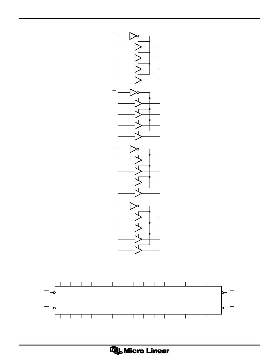
FUNCTIONAL DESCRIPTION
Figure 9. Logic Diagram
Figure 10. Logic Symbol
1A0
1OE
1B1
1B0
1A1
1B2
1A2
1B3
1A3
2A0
2OE
2B1
2B0
2A1
2B2
2A2
2B3
2A3
3A0
3OE
3B1
3B0
3A1
3B2
3A2
3B3
3A3
4A0
4OE
4B1
4B0
4A1
4B2
4A2
4B3
4A3
1A0
1B0
1A1
1B1
1A2
1B2
1A3
1B3
2A0
2A1
2A2
2A3
3A0
3A1
3A2
3A3
4A0
4A1
4A2
4A3
2B0
2B1
2B2
2B3
3B0
3B1
3B2
3B3
4B0
4B1
4B2
4B3
3OE
4OE
2OE
1OE

ML6516244
9
ARCHITECTURAL DESCRIPTION
The ML6516244 is a 16-bit buffer/line driver with 3-state
outputs designed for 3.0V to 3.6V and 4.5V to 5.5V V
CC
operation. This device is designed for Quad-Nibble,
Dual-Byte or single 16-bit word memory interleaving
operations. Each bank has an independently controlled 3-
state output enable pin with output enable/disable access
times of less than 7.0ns. Each bank is configured to have
four independent buffer/line drivers.
Until now, these buffer/line drivers were typically
implemented in CMOS logic and made to be TTL
compatible by sizing the input devices appropriately. In
order to buffer large capacitances with CMOS logic, it is
necessary to cascade an even number of inverters, each
successive inverter larger than the preceding, eventually
leading to an inverter that will drive the required load
capacitance at the required frequency. Each inverter stage
represents an additional delay in the gating process
because in order for a single gate to switch, the input must
slew more than half of the supply voltage. The best of
these 16-bit CMOS buffers has managed to drive 50pF
load capacitance with a delay of 3.6ns.
Micro Linear has produced a 16-bit buffer/line driver with
a delay less than 2.5ns by using a unique circuit
architecture that does not require cascade logic gates.
The basic architecture of the ML6516244 is shown in
Figure 11. In this circuit, there are two paths to the output.
One path sources current to the load capacitance where
the signal is asserted, and the other path sinks current from
the output when the signal is negated.
The assertion path is the Darlington pair consisting of
transistors Q1 and Q2. The effect of transistor Q1 is to
increase the current gain through the stage from input to
output, to increase the input resistance and to reduce
input capacitance. During an input low-to-high transition,
the output transistor Q2 sources large amount of current to
quickly charge up a highly capacitive load which in effect
reduces the bus settling time. This current is specified as
I
DYNAMIC
.
The negation path is also the Darlington pair consisting of
transistor Q3 and transistor Q4. With M1 connecting to
the input of the Darlington pair, Transistor Q4 then sinks a
large amount of current during the input transition from
high-to-low.
Inverter X2 is a helpful buffer that not only drives the
output toward the upper rail but also pulls the output to
the lower rail.
There are a number of MOSFETs not shown in Figure 11.
These MOSFETs are used to 3-state the buffers. For
instance, R1 and R2 were implemented as resistive
transmission gates to ensure that disabled buffers do not
load the lines of which they are connected.
OUT
V
CC
M1
IN
R1
R2
X1
X2
Q3
Q4
Q2
Q1
Figure 11. One Buffer Cell of the ML6516244

ML6516244
10
CIRCUITS AND WAVE FORMS
Figure 12. Test Circuits for All Outputs
Figure 13. Propagation Delay
V
CC
= 3V
1.5V
0V
3V
1.5V
t
PHL
t
PLH
t
RISE
AND t
FALL
INPUT = 2ns
INPUT
OUTPUT
0V
DISABLE
ENABLE
CONTROL
INPUT
OUTPUT
LOW
OUTPUT
HIGH
V
CC
= 3V
1.5V
3V
0V
VOL + 0.3V
VOL
VOH
VOH ≠ 0.3V
t
OE
t
OD
t
OD
t
OE
1.5V
1.5V
1.5V
t
OS
INPUT
OUTPUT1
OUTPUTi
i = 1 to 16
Figure 14. Enable and Disable Times
Figure 15. Output Skew
50pF
V
OUT
I
OUT
V
IN
ML6516244
DUT

ML6516244
11
PHYSICAL DIMENSIONS
inches (millimeters)
SEATING PLANE
0.291 - 0.301
(7.39 - 7.65)
0.402 - 0.410
(10.21 - 10.41)
0.620 - 0.630
(15.75 - 16.00)
0.006 - 0.014
(0.15 - 0.36)
0.024 - 0.040
(0.61 - 1.02)
0.094 - 0.110
(2.39 - 2.79)
0.008 - 0.016
(0.20 - 0.41)
0.088 - 0.092
(2.24 - 2.34)
0.005 - 0.010
(0.13 - 0.26)
0ļ - 8ļ
48
PIN 1 ID
0.025 BSC
(0.63 BSC)
0.015 - 0.025
(0.38 - 0.64)
(4 PLACES)
1
Package: R48
48-Pin SSOP
Package: T48
48-Pin TSSOP
SEATING PLANE
0.236 - 0.244
(6.00 - 6.20)
0.319 BSC
(8.1 BSC)
0.487 - 0.497
(12.37 - 12.63)
0.007 - 0.011
(0.17 - 0.27)
0.020 BSC
(0.50 BSC)
0.020 - 0.028
(0.50 - 0.70)
0.047 MAX
(1.20 MAX)
0.002 - 0.006
(0.05 - 0.15)
0.031 - 0.039
(0.80 - 1.00)
0.004 - 0.008
(0.10 - 0.20)
0ļ - 8ļ
PIN 1 ID
ML6516244
12
ORDERING INFORMATION
PART NUMBER
TEMPERATURE RANGE
PACKAGE
ML6516244CR (OBS)
0įC to 70įC
48-Pin SSOP (R48)
ML6516244CT (EOL)
0įC to 70įC
48-Pin TSSOP (T48)
DS6516244-01
Micro Linear Corporation
2092 Concourse Drive
San Jose, CA 95131
Tel: (408) 433-5200
Fax: (408) 432-0295
www.microlinear.com
© Micro Linear 2000. is a registered trademark of Micro Linear Corporation. All other trademarks are the property of their
respective owners.
Products described herein may be covered by one or more of the following U.S. patents: 4,897,611; 4,964,026; 5,027,116;
5,281,862; 5,283,483; 5,418,502; 5,508,570; 5,510,727; 5,523,940; 5,546,017; 5,559,470; 5,565,761; 5,592,128; 5,594,376;
5,652,479; 5,661,427; 5,663,874; 5,672,959; 5,689,167; 5,714,897; 5,717,798; 5,742,151; 5,747,977; 5,754,012; 5,757,174;
5,767,653; 5,777,514; 5,793,168; 5,798,635; 5,804,950; 5,808,455; 5,811,999; 5,818,207; 5,818,669; 5,825,165; 5,825,223;
5,838,723; 5.844,378; 5,844,941. Japan: 2,598,946; 2,619,299; 2,704,176; 2,821,714. Other patents are pending.