 | –≠–ª–µ–∫—Ç—Ä–æ–Ω–Ω—ã–π –∫–æ–º–ø–æ–Ω–µ–Ω—Ç: ML6652EH | –°–∫–∞—á–∞—Ç—å:  PDF PDF  ZIP ZIP |
January 2002
Preliminary Datasheet
∑ Complete implementation of fiber optic and twisted
pair media interface
∑ Intended to support ISO/IEC 8802.3, IEEE 802.3 and
TIA/EIA-785 Industry Standards, including full auto-
negotiation for twisted pair and fiber optic media
∑ 850nm, 1300nm miniature fiber optic components and
PMD modules
∑ Supports 1:1 receiver/transmitter transformer ratio for
twisted pair
∑ Low latency 10Mbps path
∑ Integrated voltage and current references
∑ Integrated twisted pair output wave shaping eliminates
external filtering
∑ Integrated twisted pair 10Base-T input filter and
100Base-TX equalizer with baseline wander correction
circuit
∑ Serial Management Interface
∑ Full and Half Duplex with Auto-Negotiation
∑ Integrated LED Driver
∑ Integrated Data Quantizer
∑ Small 44-Pin TQFP
∑ Low 3.3V operation
APPLICATIONS
∑ Single/Multi Port 10/100 Auto Negotiating Media
Converters
∑ Single/Multi Port 100Base-FX/SX to 100Base-TX Media
Converters
∑ Single/Multi Mode Fiber Converters
∑ Fiber Optic Front-End for Network Interface Cards
(NICs), Repeaters, Bridges, Hubs, Switches, and
Routers
∑ Residential Connectivity and Gateway/Demarcation
Products
∑ Redundant Link Converters
∑ Wavelength Converters
GENERAL DESCRIPTION
ML6652
10/100Mbps Ethernet Fiber and Copper
Media Converter with Auto Negotiation
FEATURES
The ML6652 is a low cost/low LED current drive single
chip Media Converter that provides 10Mbps and 100Mbps
signal conversion between twisted pair and fiber optic
Ethernet technologies. The device supports conversion
between:
10Base-T and 10Base-FL
100Base-TX and 100Base-FX/SX
100Base-FX and 100Base-SX
FLP Bursts and FLNP Bursts
The device supports 10Mbps and 100Mbps operating data
rates with Auto Negotiation using 850nm or 1300nm
optics. One or both of the fiber optic and twisted pair
interfaces can be interfaced to industry standard miniature
fiber optic components or Physical Media Dependent
(PMD) modules using Positive Emitter Coupled Logic/Low
Voltage Positive Emitter Coupled Logic (PECL/LVPECL)
compatible modes. Other wavelengths possible via
PECL/LVPECL interface.

ML6652
2
January 2002
Preliminary Datasheet
TABLE OF CONTENTS
Micro Linear makes no representations or warranties with respect to the accuracy, utility, or completeness of the contents of
this publication and reserves the right to make changes to specifications and product descriptions at any time without notice.
No license, express or implied, by estoppel or otherwise, to any patents or other intellectual property rights is granted by this
document. The circuits contained in this document are offered as possible applications only. Particular uses or applications
may invalidate some of the specifications and/or product descriptions contained herein. The customer is urged to perform its
own engineering review before deciding on a particular application. Micro Linear assumes no liability whatsoever, and
disclaims any express or implied warranty, relating to sale and/or use of Micro Linear products including liability or warranties
relating to merchantability, fitness for a particular purpose, or infringement of any intellectual property right. Micro Linear
products are not designed for use in medical, life saving, or life sustaining applications.
WARRANTY
© 2002 Micro Linear Corporation. All rights reserved. All other trademarks are the property of their respective owners.
Products described herein may be covered by one or more of the following U.S. patents: 4,897,611; 4,964,026; 5,027,116;
5,281,862; 5,283,483; 5,418,502; 5,508,570; 5,510,727; 5,523,940; 5,546,017; 5,559,470; 5,565,761; 5,592,128; 5,594,376;
5,652,479; 5,661,427; 5,663,874; 5,672,959; 5,689,167; 5,714,897; 5,717,798; 5,742,151; 5,747,977; 5,754,012; 5,757,174;
5,767,653; 5,777,514; 5,793,168; 5,798,635; 5,804,950; 5,808,455; 5,811,999; 5,818,207; 5,818,669; 5,825,165; 5,825,223;
5,838,723; 5.844,378; 5,844,941. Japan: 2,598,946; 2,619,299; 2,704,176; 2,821,714. Other patents are pending.
General Description ......................................................................................................................................................... 1
Features ........................................................................................................................................................................... 1
Applications ..................................................................................................................................................................... 1
Warranty Information ....................................................................................................................................................... 2
Block Diagram ................................................................................................................................................................. 3
Pin Configuration ............................................................................................................................................................. 4
Pin Descriptions ............................................................................................................................................................... 4
General Description ....................................................................................................................................................... 13
Functional Description ................................................................................................................................................... 14
Device Configuration ..................................................................................................................................................... 14
Default Power Configuration .......................................................................................................................................... 14
Serial Management Interface ......................................................................................................................................... 14
Speed Selection ............................................................................................................................................................. 15
Operating Modes ........................................................................................................................................................... 16
Transparent Mode ........................................................................................................................................................... 18
Fiber Optic Input/Output Interface ................................................................................................................................. 18
Power Down Mode ......................................................................................................................................................... 19
Loopback Mode ............................................................................................................................................................. 19
Scrambler/Descrambler .................................................................................................................................................. 19
Output Off Mode ........................................................................................................................................................... 19
Backup Link Mode ......................................................................................................................................................... 19
Control Registers ............................................................................................................................................................ 20
Status Registers .............................................................................................................................................................. 23
Electrical Characteristics ............................................................................................................................................... 24
Physical Dimensions ...................................................................................................................................................... 28
Order Information .......................................................................................................................................................... 28
ML6652
3
January 2002
Preliminary Datasheet
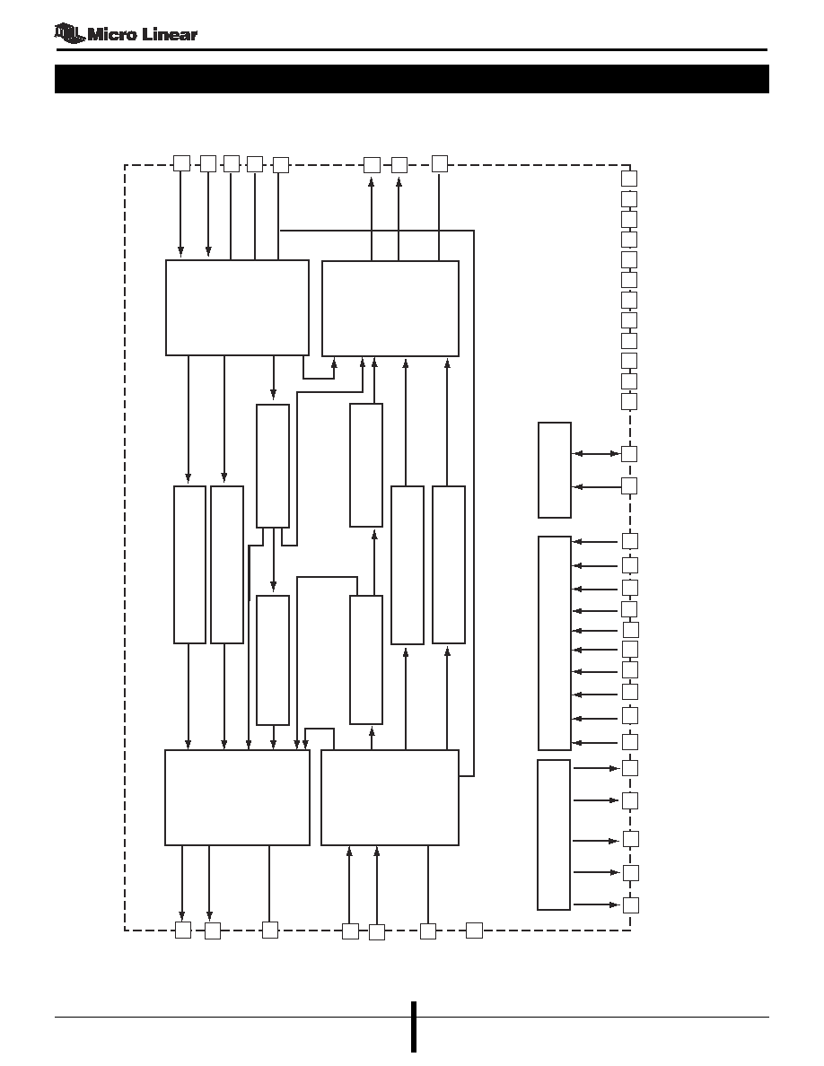
BLOCK DIAGRAM
44
42
43
41
40
24
14
13
7
8
4
5
LED STATUS &
Backup Link
Configuration
and Control Logic
Management
Interface
Twisted Pair
or
PECL/LVPECL
Output
Twisted Pair
or
PECL/LVPECL
Input
1
TPOUTP
3
38
TPOUTN
RTTP
10
TPINP
11
37
TPINN
REQSD
18
REFCLK
Auto Negotiation Processing
10M
bps
Processing
100Mbps Clock and
Data Recovery
100Base-TX
Descrambler
100M
bps
Clock and Data
Recovery
100Base-TX
Scrambler
10M
bps
Processing
Auto Negotiation Processing
Fiber Optic
or
PECL/LVPECL
Input
Fiber Optic
or
PECL/LVPECL
Output
33
FOINP
32
30
FOINN
CQOS
29
SDFO
39
21
SDTH
IOUT
22
IOUT#
36
RTOP
6
27
17
16
12
15
19
20
23
26
28
31
34
35
2
9
25
FOANDT
FOINSPD
TPANDT
TPINSPD
BCKLINK
PWRDWN#
FOOUTOFF#
TPOUTOFF#
PECLTP
PECLQU
AD4LIW
AD32
AD10
SPEED
DUPLEX
MDC
MDIO
GNDT
VCCE
GNDE
GNDD
VCCD
GNDL
VCCL
VCCFC
GNDFC
VCCQ
GNDQ
GNDB

ML6652
4
January 2002
Preliminary Datasheet
PIN CONFIGURATION
Signal names followed by "#" indicate active low input.
Pin No. Signal Name
I/O
Description
CONFIGURATION
4
AD4LIW
I
Sets the value of the Physical Layer (PHY) address bit 4 for accessing the Serial
Management Interface, and determines if the Link Integrity Warning (LIW)
function is enabled or disabled.
The Link Integrity Warning (LIW) function can only be enabled when only one
SPEED is available through setting of SPEED ( pin 27) and/or management
registers. When LIW is enabled and the input link is down at one interface to
the Media Converter, the transmitter output on that interface is turned off for
about 425ms every 3.8 seconds. It applies to both network interfaces and both
data rates. If the link at the other interface to the Media Converter is also
down, there is no output. The LIW function causes the Link Up indicator of the
link partner to blink.
Note: this pin is typically read a few microseconds after power-up, if it is tied
to supplies that do not track the ML6652 power improper results will occur.
Use VCCD (pin 19) as the pull up point, do not add decoupling capacitors to
this input pin (without thoroughly understanding your PCB layout dynamics the
safest course is to make short connections and do not add decoupling
capacitors to this input pin).
5
AD32
I
Sets the value of the PHY address bits 3 and 2 for accessing the Serial
Management Interface.
Note: this pin is typically read a few microseconds after power-up, if it is tied
to supplies that do not track the ML6652 power improper results will occur.
Use VCCD (pin 19) as the pull up point, do not add decoupling capacitors to
this input pin (without thoroughly understanding your PCB layout dynamics the
safest course is to make short connections and do not add decoupling
capacitors to this input pin).
TOP VIEW
ML6652
44-Pin TQFP (H44-10)
FOINP
FOINN
VCCQ
CQOS
SDFO
GNDFC
SPEED
VCCFC
DUPLEX
PWRDWN#
VCCL
TPOUTP
GNDT
TPOUTN
AD4LIW
AD32
AD10
PECLTP
PECLQU
VCCE
TPINP
TPINN
12 13 14 15 16
FOANDT
TPANDT
FOINSPD
TPINSPD
BCKPLINK
SDTH
RTTP
REQSD
RTOP
GNDB
GNDQ
GNDE
TPOUTOFF#
FOOUTOFF#
GNDD
MDIO
MDC
REFCLK
VCCD
GNDL
IOUT
IOUT#
17 18
1
2
3
4
5
6
7
8
9
10
11
44 43 42 41 40
33
32
31
30
29
28
27
26
25
24
23
39 38
19
37
20
36
21
35
22
34
PIN DESCRIPTIONS

ML6652
5
January 2002
Preliminary Datasheet
PIN DESCRIPTIONS (continued)
Pin No. Signal Name
I/O
Description
6
AD10
I
Sets the value of the PHY address bits 1 and 0 for accessing the Serial
Management Interface.
Note: this pin is typically read a few microseconds after power-up, if it is tied
to supplies that do not track the ML6652 power improper results will occur.
Use VCCD (pin 19) as the pull up point, do not add decoupling capacitors to
this input pin (without thoroughly understanding your PCB layout dynamics the
safest course is to make short connections and do not add decoupling
capacitors to this input pin).
7
PECLTP
I
The copper interface is selected as shown in Table 2. When twisted pair
interface is selected, the scrambler and descrambler are enabled by default
and can be disabled with a management register bit.
When using twisted pair interface, this pin also defines the maximum
supported link distance. When the 10 meters maximum link length is selected,
the input is not equalized before being sliced.
Note: this pin is typically read a few microseconds after power-up, if it is tied
to supplies that do not track the ML6652 power improper results will occur.
Use VCCD (pin 19) as the pull up point, do not add decoupling capacitors to
this input pin (without thoroughly understanding your PCB layout dynamics the
safest course is to make short connections and do not add decoupling
capacitors to this input pin).
e
m
a
N
n
i
P
W
I
L
4
D
A
2
3
D
A
0
1
D
A
l
e
v
e
L
t
u
p
n
I
n
o
i
t
c
n
u
F
W
I
L
t
i
B
4
D
A
Y
H
P
t
i
B
3
D
A
Y
H
P
t
i
B
2
D
A
Y
H
P
t
i
B
1
D
A
Y
H
P
t
i
B
0
D
A
Y
H
P
0
d
e
l
b
a
s
i
D
0
0
0
0
0
C
C
V
f
o
3
/
1
d
e
l
b
a
n
E
0
1
0
1
0
C
C
V
f
o
3
/
2
d
e
l
b
a
n
E
1
1
1
1
1
C
C
V
d
e
l
b
a
s
i
D
1
0
1
0
1
Table 1.
P
T
L
C
E
P
t
a
s
e
c
a
f
r
e
t
n
I
d
n
a
N
N
I
P
T
/
P
N
I
P
T
N
T
U
O
P
T
/
P
T
U
O
P
T
P
T
L
C
E
P
>
3
.
0
3
<
t
l
u
a
f
e
D
h
t
g
n
e
L
r
e
p
p
o
C
P
T
T
R
O
H
S
>
2
.
0
3
<
t
l
u
a
f
e
D
t
n
e
r
r
u
C
t
u
p
t
u
O
T
U
O
P
T
I
W
O
L
>
4
.
0
3
<
t
l
u
a
f
e
D
0
r
i
a
P
d
e
t
s
i
w
T
0
X
T
-
e
s
a
B
0
0
1
d
r
a
d
n
a
t
S
0
d
r
a
d
n
a
t
S
0
C
C
V
f
o
3
/
1
L
C
E
P
V
L
/
L
C
E
P
1
s
e
c
a
r
T
B
C
P
0
A
N
0
C
C
V
f
o
3
/
2
r
i
a
P
d
e
t
s
i
w
T
0
s
e
c
a
r
T
B
C
P
1
w
o
L
1
C
C
V
r
i
a
P
d
e
t
s
i
w
T
0
m
0
1
1
d
r
a
d
n
a
t
S
0
Table 2.

ML6652
6
January 2002
Preliminary Datasheet
Note: The ML6652 fiber interface quantizer sensitivity can be adjusted via
Register 30 bits 5, 6 and 7 to accomodate various cable lengths and signal
intensity.
25
DUPLEX
I
This input can have one of three levels: VCC, VCC/2 or 0 Volts. This input has
80K ohm resistors internally connected to both VCC and Ground, generating
VCC/2 at the input if left unconnected. Settings defined by the DUPLEX power
up preset pin can be over written by the management interface. At power up
the DUPLEX pin causes the following default values to be written to
management register 30.
Note: this pin is typically read a few microseconds after power-up, if it is tied
to supplies that do not track the ML6652 power improper results will occur.
Use VCCD (pin 19) as the pull up point, do not add decoupling capacitors to
this input pin (without thoroughly understanding your PCB layout dynamics the
safest course is to make short connections and do not add decoupling
capacitors to this input pin).
Pin No. Signal Name
I/O
Description
8
PECLQU
I
The fiber interface is selected as shown in Table 3.
When using an LED driver and fiber optic receiver, this pin also defines the
maximum supported link distance.
When the 300m maximum link length is selected, the voltage thresholds for
Signal Detect are increased.
PIN DESCRIPTIONS (continued)
U
Q
L
C
E
P
t
a
s
e
c
a
f
r
e
t
n
I
d
n
a
N
N
I
O
F
/
P
N
I
O
F
#
T
U
O
I
/
T
U
O
I
U
Q
L
C
E
P
>
7
.
0
3
<
t
l
u
a
f
e
D
c
i
t
p
O
r
e
b
i
F
h
t
g
n
e
L
k
n
i
L
e
s
a
B
0
0
1
/
e
s
a
B
0
1
O
F
T
R
O
H
S
>
5
.
0
3
<
t
l
u
a
f
e
D
h
t
g
n
e
L
e
v
a
W
L
W
G
N
O
L
>
6
.
0
3
<
t
l
u
a
f
e
D
0
D
E
L
d
n
a
r
e
z
i
t
n
a
u
Q
r
e
v
i
r
D
0
m
0
0
3
/
m
K
2
0
m
n
0
5
8
0
C
C
V
f
o
3
/
1
L
C
E
P
V
L
/
L
C
E
P
1
s
e
c
a
r
T
B
C
P
0
A
N
0
C
C
V
f
o
3
/
2
D
E
L
d
n
a
r
e
z
i
t
n
a
u
Q
r
e
v
i
r
D
0
m
K
2
/
m
K
2
0
m
n
0
0
3
1
1
C
C
V
D
E
L
d
n
a
r
e
z
i
t
n
a
u
Q
r
e
v
i
r
D
0
m
0
0
3
/
m
0
0
3
1
m
n
0
0
3
1
r
o
0
5
8
0
Table 3.
Table 4.
e
g
a
t
l
o
V
X
E
L
P
U
D
#
T
N
E
R
A
P
S
N
A
R
T
t
l
u
a
f
e
D
>
1
1
.
0
3
<
#
D
F
T
R
E
V
D
A
t
l
u
a
f
e
D
>
0
1
.
0
3
<
#
D
H
T
R
E
V
D
A
t
l
u
a
f
e
D
>
5
1
.
0
3
<
0
1
1
0
2
/
C
C
V
0
0
0
C
C
V
1
0
0

ML6652
7
January 2002
Preliminary Datasheet
PIN DESCRIPTIONS (continued)
Pin No. Signal Name
I/O
Description
Table 5.
e
g
a
t
l
o
V
D
E
E
P
S
>
4
1
.
0
3
<
N
A
L
B
S
D
t
l
u
a
f
e
D
>
9
.
0
3
<
D
E
E
P
S
E
L
G
N
I
S
t
l
u
a
f
e
D
>
8
.
0
3
<
s
p
b
M
0
1
L
E
S
t
l
u
a
f
e
D
0
1
1
1
2
/
C
C
V
0
0
0
C
C
V
1
1
0
Table 6.
DUPLEX and SPEED can be used concurrently to set the power up mode of the
ML6652 see Tables 4 and 6. For Mode details see the General Description
section of this data sheet.
27
SPEED
I
This input can have one of three levels: VCC, VCC/2, and 0Volts. The input has
80K
resistors internally connected to both VCC and Ground generating VCC/2
at the input left unconnected. Settings defined by the SPEED power up preset
pin can be over written by the management interface. At power up the SPEED
pin causes the following default values to be written to management register
30.
Note: this pin is typically read a few microseconds after power-up. If it is tied
to supplies that do not track the ML6652 power, improper results will occur.
Use VCCD (pin 19) as the pull up point, do not add decoupling capacitors to
this input pin (without thoroughly understanding your PCB layout dynamics the
safest course is to make short connections and do not add decoupling
capacitors to this input pin).
e
d
o
M
y
r
a
m
m
u
S
g
n
i
t
a
r
e
p
O
e
g
a
t
l
o
V
D
E
E
P
S
e
g
a
t
l
o
V
X
E
L
P
U
D
0
1
d
e
c
r
o
F
e
d
o
m
X
E
L
P
U
D
e
h
T
.
e
l
b
a
l
i
a
v
a
y
l
n
o
e
t
a
r
a
t
a
d
s
p
b
M
0
1
.
s
r
e
n
t
r
a
p
k
n
i
l
e
h
t
y
b
d
e
t
c
e
l
e
s
s
i
0
e
r
a
C
t
'
n
o
D
0
0
1
d
e
c
r
o
F
e
d
o
m
X
E
L
P
U
D
e
h
T
.
e
l
b
a
l
i
a
v
a
y
l
n
o
e
t
a
r
a
t
a
d
s
/
b
M
0
0
1
.
s
r
e
n
t
r
a
p
k
n
i
l
e
h
t
y
b
d
e
t
c
e
l
e
s
s
i
C
C
V
e
r
a
C
t
'
n
o
D
t
n
e
r
a
p
s
n
a
r
T
-
n
o
N
X
E
L
P
U
D
-
f
l
a
H
0
1
h
t
o
B
.
d
e
s
i
t
r
e
v
d
a
e
r
a
s
e
d
o
m
X
E
L
P
U
D
-
f
l
a
H
e
h
t
y
l
n
O
a
t
a
d
e
h
t
y
l
n
O
.
e
l
b
a
l
i
a
v
a
e
r
a
s
e
t
a
r
a
t
a
d
s
p
b
M
0
0
1
d
n
a
r
e
b
i
f
e
h
t
t
a
t
n
e
s
e
r
p
y
g
o
l
o
n
h
c
e
t
e
h
t
o
t
t
n
e
l
a
v
i
u
q
e
e
t
a
r
.
d
e
s
i
t
r
e
v
d
a
s
i
e
c
a
f
r
e
t
n
i
t
u
p
n
i
c
i
t
p
o
2
/
C
C
V
0
t
n
e
r
a
p
s
n
a
r
T
-
n
o
N
d
n
a
X
E
L
P
U
D
-
f
l
a
H
h
t
o
B
.
d
e
t
a
r
e
n
e
g
e
r
a
s
t
s
r
u
B
P
L
F
d
n
a
0
1
h
t
o
B
.
d
e
s
i
t
r
e
v
d
a
e
r
a
s
e
d
o
m
X
E
L
P
U
D
-
l
l
u
F
e
t
a
r
a
t
a
d
e
h
t
y
l
n
O
.
e
l
b
a
l
i
a
v
a
e
r
a
s
e
t
a
r
a
t
a
d
s
p
b
M
0
0
1
c
i
t
p
o
r
e
b
i
f
e
h
t
t
a
t
n
e
s
e
r
p
y
g
o
l
o
n
h
c
e
t
e
h
t
o
t
t
n
e
l
a
v
i
u
q
e
.
d
e
s
i
t
r
e
v
d
a
s
i
e
c
a
f
r
e
t
n
i
t
u
p
n
i
2
/
C
C
V
C
C
V
t
n
e
r
a
p
s
n
a
r
T
,
s
p
b
M
0
1
r
e
y
a
l
-
b
u
s
n
o
i
t
a
i
t
o
g
e
N
-
o
t
u
A
d
r
a
d
n
a
t
S
r
e
n
t
r
a
p
k
n
i
l
d
n
e
r
a
f
n
o
i
t
a
i
t
o
g
e
N
-
o
t
u
A
d
n
a
s
p
b
M
0
0
1
.
e
l
b
a
l
i
a
v
a
g
n
i
l
a
n
g
i
s
2
/
C
C
V
2
/
C
C
V

ML6652
8
January 2002
Preliminary Datasheet
PIN DESCRIPTIONS (continued)
Pin No. Signal Name
I/O
Description
CONTROL
13
TPOUTOFF#
I (CMOS)
Active low, the output stage of the twisted pair output is turned off. If not
connected they are pulled high by internal resistors
14
FOOUTOFF#
I (CMOS)
Active low, the output stage of the fiber optic output is turned off. If not
connected they are pulled high by internal resistors
24
PWRDWN#
I (CMOS)
Active low, all the circuits are powered down. Configuration pins are read and
register bits are initialized 3 to 8
µ
s after a rising edge of PWRDWN#. If not
connected they are pulled high by internal resistors
DATA SIGNAL INPUT/OUTPUT
1
TPOUTP
O
The two operating modes available for these pins are selected with the
configuration pin PECLTP (pin 7) or the configuration bit PECLTP <30.3>
3
TPOUTN
O
Twisted Pair Interface Mode:
Transmit twisted pair positive and complementary outputs. These outputs form
a differential current output pair that drives Multi Level Transition (MLT-3)
waveforms into the network coupling transformer during 100Mbps mode,
Manchester encoded 10Base-T data or Normal Line Pulses (NLPs) during
10Mbps mode, and Fast Link Pulse (FLP) Bursts during Auto-Negotiation.
TPOUTP and TPOUTN must have external pull up resistors to VCC (refer to
description of RTTP pin)
PECL/LVPECL Compatible Interface Mode:
PECL/LVPECL interface positive and complementary outputs. These outputs
form a differential current output pair that drives Non Return to Zero Inverted
(NRZI) encoded 100Base-FX or 100Base-SX symbols during 100Mbps mode,
Manchester encoded 10Base-FL data or OPT_IDL during 10Mbps mode, and
Fiber Link Negotiation Pulse (FLNP) Bursts during Auto-Negotiation. TPOUTP
and TPOUTN must have external pull up resistors to VCC and be AC coupled
to the inputs of a fiber optic PMD module (refer to description of RTTP pin). A
resistor network may be needed to setup the common mode voltage at the
input pins of the PMD module
38
RTTP
I
Twisted pair PECL/LVPECL compatible driver bias resistor. An external resistor
connected between RTTP and ground sets a constant bias current for the
differential output driver circuitry TPOUTP/TPOUTN.
These output currents depend on the operating mode.
The recommended external component values are:
Twisted Pair Mode:
2K
,
1%, between RTTP and ground
50
,
1%, between TPOUTP and VCC
50
,
1%, between TPOUTN and VCC
PECL Compatible mode:
2K
,
1%, between RTTP and ground
62
,
1%, between TPOUTP and VCC
62
,
1%, between TPOUTN and VCC
Also AC coupled to the PMD inputs
10
TPINP
I
The two operating modes available for these pins are selected with the
configuration pin PECLTP (Pin 7) or the configuration bit PECLTP <30.3>.
11
TPINN
I
Twisted Pair Interface Mode:
Receive twisted pair positive and complementary inputs. These inputs form a
differential input pair that receives 100Base-TX, FLP Burst, or 10Base-T signal
from the network. The common mode voltage is set internally and the
differential input resistance is about 2K
.
The twisted pair interface requires a network consisting of a 1500Pf capacitor
and a 200
resistor in parallel; in series with each pin 10 and 11 as shown in
Figure 1.

ML6652
9
January 2002
Preliminary Datasheet
PIN DESCRIPTIONS (continued)
Pin No. Signal Name
I/O
Description
Figure 1. Twisted Pair Interface Mode Input Networks
1500pF
1500pF
200
200
10
11
ML6652
From Input
Transformer Circuit
Pulse H1019 or equivalent
PECL/LVPECL Compatible Interface Mode:
PECL/LVPECL compatible interface positive and complementary inputs. These
inputs form a differential input pair that receives 100Base-FX, 100Base-SX,
FLNP Bursts, or 10Base-FL signal from a fiber optic PMD. The PMD outputs
should be AC coupled to these inputs with .1µF capacitors. The common mode
voltage is set internally with ~1K
or so resistors from each input pin to an on-
chip voltage reference. The positive output of the PMD (high during the high-
light state) must connect to TPINP and the complementary output of the PMD
must connect to TPINN
37
REQSD
I
The two operating modes available for this pin are selected with the
configuration pin PECLQU or the configuration bit PECLQU <30.2>
Twisted Pair Interface Mode:
Equalizer bias resistor pin. An external resistor connected between this pin and
ground sets internal currents that control the receiver's adaptive equalizer
transfer function. The recommended resistor value is 5K
,
1%
PECL/LVPECL Compatible Interface Mode:
This input pin is connected to the Signal Detect (SD) output of a fiber optic
PMD module. The voltage level at this pin is compared to the voltage level at
pin SDTH to determine the logic value. If it is lower, then the input at TPINP/
TPINN is rejected. If it is higher, then the input at TPINP/TPINN is passed to the
internal circuits
39
SDTH
I
The voltage at this pin is a single ended PECL/LVPECL reference. Refer to
description of SDFO and REQSD pins. This pin is not used if the TPINP/TPINN
interface or the FOINP/FOINN are not setup for PECL/LVPECL compatible
mode. In such a case, the SDTH pin should be set to VCC
21
IOUT
O
The two operating modes available for these pins are selected with the
configuration pin PECLQU or the configuration bit PECLQU <30.7>
22
IOUT#
O
Fiber Optic Interface Mode:
IOUT (pin 21) becomes the output connection to the cathode of an external
fiber optic LED. The output data is NRZI encoded 100Base-FX or 100Base-SX
symbols during 100Mbps mode, Manchester encoded 10Base-FL data or
OPT_IDL (10Base-FL idle signal) during 10Mbps mode, and FLNP Bursts during
Auto-Negotiation.

ML6652
10
January 2002
Preliminary Datasheet
IOUT# (pin 22) is optionally used to provide current peaking. If peaking is
implemented, a 1K
off-chip resistor should be connected to ground and a 1nF
capacitor connected to IOUT. These components determine the peaking
current waveform. When peaking is not used, IOUT# should connect to VCC
PECL/LVPECL Compatible Interface Mode:
PECL/LVPECL interface positive and complementary outputs. These outputs
form a differential current output pair that drives NRZI encoded 100Base-SX or
100Base-FX symbols during 100Mbps mode, Manchester encoded 10Base-FL
data or OPT_IDL during 10Mbps mode, and FLNP Bursts during Auto-
Negotiation. IOUT and IOUT# are loaded with external resistors to VCC and
AC coupled to the inputs of a fiber optic PMD module (refer to description of
RTOP pin). A resistor network may be needed to setup the common mode
voltage at the input pins of the PMD module
36
RTOP
O
Fiber optic LED or PECL/LVPECL driver bias resistor. An external resistor
connected between RTOP and ground sets a constant bias current for the single
ended LED driver or differential PECL/LVPECL driver circuitry. These output
currents depend on the operating mode.
The recommended external component values are:
Fiber Optic Interface mode: (1% resistors, +/- 10% currents)
Indicated is the current into pin IOUT during the High-Light state.
2.8K
between RTOP and ground for 50mA.
2K
between RTOP and ground for 70mA.
1.4K
between RTOP and ground for 100mA.
PECL/LVPECL Interface mode:
1.4K
, 1%, between RTOP and ground for 10mA tail current.
62
, 1%, between IOUT and VCC.
62
, 1%, between IOUT# and VCC.
Also AC coupled to PMD inputs
33
FOINP
I
The two operating modes available for these pins and are selected with the
configuration pin PECLQU or the configuration bit PECLQU <30.7>
32
FOINN
I
Fiber Optic Interface Mode:
Fiber optic quantizer positive and complementary inputs. FOINP is
capacitively coupled to the output of a fiber optic receiver, while FOINN is
capacitively coupled to the VCC of the fiber optic receiver. Recommended
capacitor values: 10nF, 5%. FOINP voltage must be higher during the "high
light" state than during the low-light state
PECL/LVPECL Compatible Interface Mode:
PECL/LVPECL interface positive and complementary inputs. These inputs form
a differential input pair that receives 100Base-FX, 100Base-SX, FLNP Bursts, or
10Base-FL signal from a fiber optic PMD. The PMD outputs are AC coupled to
these inputs with 10nF, 5% capacitors. The common mode voltage is set
internally with ~900
(or so) resistors from each input pin to an on-chip
voltage reference. FOINP voltage must be higher during the "high light" state
than during the low-light state
30
CQOS
Data quantizer offset cancellation loop capacitor. An external capacitor
between this pin and VCC determines the dominant pole of the offset
cancellation feedback loop. The recommended value is .1µF, 10%
PIN DESCRIPTIONS (continued)
Pin No. Signal Name
I/O
Description

ML6652
11
January 2002
Preliminary Datasheet
PIN DESCRIPTIONS (continued)
Pin No. Signal Name
I/O
Description
29
SDFO
I
The two operating modes available for this pin are selected with the
configuration pin PECLQU or the configuration bit PECLQU <30.2>
Fiber Optic Interface Mode:
This pin is not used and should be connected to VCC.
PECL/LVPECL Compatible Interface Mode:
This input pin is connected to the Signal Detect (SD) output of a fiber optic
PMD. The voltage level at this pin is compared to the voltage level at pin
SDTH to determine the logic value. If it is lower than the input at FOINP/
FOINN is rejected. If it is higher than the input at FOINP/FOINN is passed to
the internal circuits.
BACKUP LINK FUNCTION
40
BCKPLINK
I/O
INPUT MODE:
At power up, pin 40 (BCKPLINK) is read and the BCKPDIS register <28.1> is set
appropriately. A high (VCC) at power up causes Register 28, Bit 1 (BCKPDIS)
to be set high (1) disabling the Back-up link function. BCKPDIS can
subsequently be over written by the management interface at any time.
Note: This pin is typically read a few microseconds after power-up, if it is tied
to supplies that do not track the ML6652 power, improper results may occur.
For BCKPLINK, use VCCD (pin 19) as the pull up point, do not add decoupling
capacitors to Pin 40 (without thoroughly understanding your PCB layout power
up dynamics the safest course is to make short connections and do not add
decoupling capacitors to this pin).
OUTPUT MODE:
After power-up, BCKPLINK is used as an output. It is Active high to enable a
secondary fiber link via a second ML6652 device (see Functional Description,
Backup Link Mode in this data sheet for details).
Use this function in forced 100Mbps mode, non loopback only
LED STATUS
41
TPINSPD
O
This output goes high to indicate that a 100Mbps signal is present at the TPINP/
TPINN interface, and it goes low to indicate that a 10Mbps signal is present at
the TPINP/TPINN interface. The signal can be idle or packets. This pin is set to
high impedance otherwise.
42
FOINSPD
O
This output goes high to indicate that a 100Mbps signal is present at the
FOINP/FOINN interface, and it goes low to indicate that a 10Mbps signal is
present at the FOINP/FOINN interface. The signal can be idle or packets. This
pin is set to high impedance otherwise.
43
TPANDT
O
When TPINSPD is in the high impedance state, no 10 or 100Mbps signal at
TPINP/TPINN, the TPANDT LED pulls low while receiving Auto-Negotiation
signal at the TPINP/TPINN interface. When TPINSPD is not in the high
impedance state, the TPANDT pin pulls low to indicate that a data packet is
being detected at the TPINP/TPINN interface. When a data packet is indicated,
the pulse width at TPANDT is stretched to a minimum of 1.3 to 2.7ms to
improve visibility. This low current LED driver interface requires a 10K
pull-
up resistor and a small CMOS buffer as shown in Figure 2. In any other case
this pin is in high impedance state.
10K
TPAN_DT
VCCD
VCCD
560
TPAN_DT
LED
CMOS Buffer, Fairchild NC7WZ16 or Equivalent,
Buffer VCC=VCCD, Buffer Ground = DGND
43
Figure 2.

ML6652
12
January 2002
Preliminary Datasheet
LED STATUS (CONTINUED)
44
FOANDT
O
When FOINSPD is in the high impedance state, no 10 or 100Mbps signal at
FOINP/FOINN, the FOANDT LED pulls low while receiving Auto-Negotiation
signal at the FOINP/FOINN interface. When FOINSPD is not in the high
impedance state, the FOANDT pin pulls low to indicate that a data packet is
being detected at the FOINP/FOINN interface. When a data packet is
indicated, the pulse width at FOANDT is stretched to a minimum of 1.3 to
2.7ms to improve visibility. This low current LED driver interface requires a
10K
pull-up resistor and a small CMOS buffer as shown in Figure 3. In any
other case this pin is in high impedance state.
MANAGEMENT INTERFACE
16
MDIO
Management data TTL compatible input/output pin. Connect to ground if
unused
17
MDC
Management clock TTL input. The maximum frequency can be 12.5MHz
instead of the 2.5MHz limit of IEEE 802.3. Connect to ground if unused
REFERENCE CLOCK
18
REFCLK
25MHz Reference Clock CMOS input. This clock is used for internal digital
logic, and as a reference for the PLLs.
POWER AND GROUND
2
GNDT
Ground for the twisted pair driver output stage.
12
GNDE
Ground for the equalizer, one PLL and part of the descrambler and twisted pair
driver.
15
GNDD
Ground for CMOS noisy circuits.
20
GNDL
Ground for the fiber optic LED driver output stage.
28
GNDFC
Ground for one PLL, part of the scrambler, fiber optic LED driver, and
quantizer.
34
GNDQ
Ground for the quantizer and central bias.
35
GNDB
Ground for part of the central biasing.
9
VCCE
Power supply for the equalizer, one PLL and part of the descrambler and
twisted pair driver.
19
VCCD
Power supply for CMOS noisy circuits.
23
VCCL
Power supply for the fiber optic LED driver output stage.
26
VCCFC
Power supply for one PLL, part of the scrambler, fiber optic LED driver, and
quantizer.
31
VCCQ
Power supply for the quantizer and central bias.
PIN DESCRIPTIONS (continued)
Pin No. Signal Name
I/O
Description
10K
FOAN_DT
VCCD
VCCD
560
FOAN_DT
LED
CMOS Buffer, Fairchild NC7WZ16 or Equivalent,
Buffer VCC=VCCD, Buffer Ground = DGND
44
Figure 3.

ML6652
13
January 2002
Preliminary Datasheet
GENERAL DESCRIPTION
The ML6652 Fast Ethernet Media Converter provides
signal conversion between the following standards:
∑
10BASE-T to 10BASE-FL; (10Mbps twisted pair copper
media and 10Mbps 850nm fiber media)
∑
Proprietary 10BASE-T to 10BASE-1300nm Fiber;
(10Mbps twisted pair copper media and 10Mbps
1300nm fiber media).
∑
100BASE-TX to 100BASE-SX/FX (100Mbps twisted pair
copper media and 1300nm or 850nm fiber media).
∑
100BASE-FX to 100BASE-SX (100Mbps 850nm fiber
media and 100Mbps 1300nm fiber media).
The ML6652 supports conversion between Twisted Pair
Side, Fast Link Pulses (FLP) and Fiber Side, Fiber Link
Negotiation Pulses (FLNP). It supports ISO/IEC 8802.3,
IEEE 802.3, and TIA/EIA-785 including Auto-Negotiation
on both twisted pair and fiber optics.
The ML6652 data interfaces can all be configured in a
number of ways. The twisted pair inputs and outputs can
be configured in Twisted Pair Mode to interface with a 1:1
transformer for transmit and receive or in PECL/LVPECL
Mode to interface a PMD module. The fiber optic inputs
and outputs can be configured in Quantizer/Fiber Optic
Mode with an LED driver or in PECL/LVPECL Mode. LED
status outputs identify internal operational status.
The ML6652 operating modes are configurable through
control input pins (at power up) or through management
control registers that are programmable through an
interface protocol compatible with MII Serial
Management Interface as defined in IEEE 802.3-1998
standards.
CONFIGURABLE MODES
Operating Modes (Forced, Transparent And Non-
transparent)
1) FORCED 10Mbps only mode,
2) FORCED 100Mbps only mode,
3) NON-TRANSPARENT Half Duplex only, with Auto-
Negotiation
4) NON-TRANSPARENT Full and Half Duplex with Auto-
Negotiation
5) TRANSPARENT 10/100Mbps with Auto-Negotiation
6) NON-TRANSPARENT Special case
Interface Modes
1) Twisted pair interface
a)
Twisted Pair (Transformer input) Mode or
b)
PECL/LVPECL Mode
b) Fiber Optic Interface
i)
Quantizer/Fiber Optic LED Driver Mode or
ii) PECL/LVPECL Mode
Special Modes
1) Power Down Mode
a)
Configurable through:
(i) Control pin 24 or
(ii) Management control register
2) Loopback Test Modes
a)
For the fiber optic interface or
b)
The twisted pair interface
c)
Both are configurable through the Management
control register and include bypassing clock and
data recovery blocks.
3) Transmitter Output Off Mode:
a)
Twisted Pair or
b)
Fiber Optic
c)
Both are configurable through the Management
control registers or control pins TPOUTOFF# (pin
13) and FOOUTOFF# (pin 14).
4) Backup Link Mode
a)
Configurable through Management control
register or via BCKPLINK (Pin 40).
ML6652
14
January 2002
Preliminary Datasheet
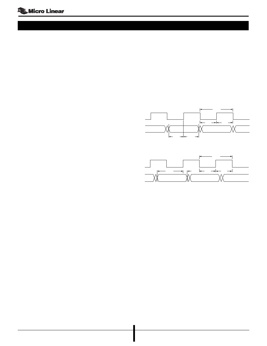
SERIAL MANAGEMENT INTERFACE
The ML6652 has management functions controlled by
three sixteen bit registers and status updated by one
sixteen bit registers. Management Data is input and
output through MDIO and clocked by MDC in an
interface compatible with the protocol defined in clause
22 of IEEE Std 802.3-1998 MII Serial Management
Interface. The address bits PHYAD <4:0> are determined
by voltage levels at configuration pins AD4LIW, AD32,
and AD10.
Management interface read and write timing relationships
are shown in Figures 4 and 5.
FUNCTIONAL DESCRIPTION
MDIO
MDC
t
SPWS
t
SPWH
t
CPW
t
CPW
t
CPER
MDIO
MDC
t
SPRH
t
CPW
t
CPW
t
SPRS
t
CPER
DEVICE CONFIGURATION
Configuring the ML6652 Media Converter is
accomplished through input configuration pins or bits in
management control register 30. Configuration pins
AD4LIW, AD32 and AD10 determine the PHY address
used with the serial management interface consisting of
MDIO (pin 16) and MDC (pin 17). The setting of any R/W
bit in the control management registers can be modified
by writing data to the register through the serial
management interface. The control management registers
27, 28, 30, and 31 always indicate the current operating
mode of the ML6652.
The PHY address settings defined by AD4LIW (pin 4),
AD32 (pin 5), and AD10 (pin 6) are not latched and must
remain stable during any serial management interface
read or write operation. The PHY address pins each have
four (4) distinct input levels and together encode the
required five (5) bit PHY addresses. Nominal values of
VCC and 0V are obtained with directions to VCCD or
GNDD. Nominal values of 2/3 VCC and 1/3 VCC must be
developed with external resistor dividers.
Input pins SPEED (pin 27) and DUPLEX (pin 25) are three
level inputs having internal 80K
resistors connected to
both VCC and Ground. Nominal input voltage levels are
VCC, VCC/2, when input is left floating, and Ground. The
state of configuration pins DUPLEX, SPEED, PECLTP (pin
7) PECLQU (pin 8), and AD4LIW (pin 4) are latched 3µ to
8µs after:
1) system power up (internal signal POR going low)
2) trailing edge of PWRDWN# (pin 24) Ground to VCC
3) reset <30.13> is cleared.
Input pins PECLTP (pin 7) and PECLQU (pin 8) are 4 level
input pins with no internal pull-up or pull-down resistors
connected. Nominal values of VCC and 0V are obtained
with directions to VCC or Ground. Nominal values of 2/3
VCC and 1/3 VCC must be developed with external
resistor dividers.
DEFAULT POWER ON CONFIGURATION
This configuration method can be used to set the device
whenever the MII serial management interface is not
available. The logic levels at configuration pins DUPLEX,
SPEED, PECLTP, PECLQU and AD4LIW are decoded and
latched in management control registers 28, 30 and 31
after system power up or after a (low) to (high) transition
at PWRDWN#.
Figure 4. Write
Figure 5. Read

ML6652
15
January 2002
Preliminary Datasheet
SPEED SELECTION
The Operating modes, FORCED, TRANSPARENT and
NON-TRANSPARENT are chosen at power up by setting of
the DUPLEX and SPEED pins. Thereafter the operating
modes may be set by toggling bits in management register
30.
DUPLEX and SPEED must be used concurrently to set the
mode of the ML6652 see Tables 7 and 8.
FUNCTIONAL DESCRIPTION
e
d
o
M
y
r
a
m
m
u
S
g
n
i
t
a
r
e
p
O
e
g
a
t
l
o
V
D
E
E
P
S
e
g
a
t
l
o
V
X
E
L
P
U
D
0
1
d
e
c
r
o
F
e
d
o
m
X
E
L
P
U
D
e
h
T
.
e
l
b
a
l
i
a
v
a
y
l
n
o
e
t
a
r
a
t
a
d
s
p
b
M
0
1
.
s
r
e
n
t
r
a
p
k
n
i
l
e
h
t
y
b
d
e
t
c
e
l
e
s
s
i
0
e
r
a
C
t
'
n
o
D
0
0
1
d
e
c
r
o
F
e
d
o
m
X
E
L
P
U
D
e
h
T
.
e
l
b
a
l
i
a
v
a
y
l
n
o
e
t
a
r
a
t
a
d
s
/
b
M
0
0
1
.
s
r
e
n
t
r
a
p
k
n
i
l
e
h
t
y
b
d
e
t
c
e
l
e
s
s
i
C
C
V
e
r
a
C
t
'
n
o
D
t
n
e
r
a
p
s
n
a
r
T
-
n
o
N
X
E
L
P
U
D
-
f
l
a
H
0
1
h
t
o
B
.
d
e
s
i
t
r
e
v
d
a
e
r
a
s
e
d
o
m
X
E
L
P
U
D
-
f
l
a
H
e
h
t
y
l
n
O
a
t
a
d
e
h
t
y
l
n
O
.
e
l
b
a
l
i
a
v
a
e
r
a
s
e
t
a
r
a
t
a
d
s
p
b
M
0
0
1
d
n
a
r
e
b
i
f
e
h
t
t
a
t
n
e
s
e
r
p
y
g
o
l
o
n
h
c
e
t
e
h
t
o
t
t
n
e
l
a
v
i
u
q
e
e
t
a
r
.
d
e
s
i
t
r
e
v
d
a
s
i
e
c
a
f
r
e
t
n
i
t
u
p
n
i
c
i
t
p
o
2
/
C
C
V
0
t
n
e
r
a
p
s
n
a
r
T
-
n
o
N
d
n
a
X
E
L
P
U
D
-
f
l
a
H
h
t
o
B
.
d
e
t
a
r
e
n
e
g
e
r
a
s
t
s
r
u
B
P
L
F
d
n
a
0
1
h
t
o
B
.
d
e
s
i
t
r
e
v
d
a
e
r
a
s
e
d
o
m
X
E
L
P
U
D
-
l
l
u
F
e
t
a
r
a
t
a
d
e
h
t
y
l
n
O
.
e
l
b
a
l
i
a
v
a
e
r
a
s
e
t
a
r
a
t
a
d
s
p
b
M
0
0
1
c
i
t
p
o
r
e
b
i
f
e
h
t
t
a
t
n
e
s
e
r
p
y
g
o
l
o
n
h
c
e
t
e
h
t
o
t
t
n
e
l
a
v
i
u
q
e
.
d
e
s
i
t
r
e
v
d
a
s
i
e
c
a
f
r
e
t
n
i
t
u
p
n
i
2
/
C
C
V
C
C
V
t
n
e
r
a
p
s
n
a
r
T
,
s
p
b
M
0
1
r
e
y
a
l
-
b
u
s
n
o
i
t
a
i
t
o
g
e
N
-
o
t
u
A
d
r
a
d
n
a
t
S
r
e
n
t
r
a
p
k
n
i
l
d
n
e
r
a
f
n
o
i
t
a
i
t
o
g
e
N
-
o
t
u
A
d
n
a
s
p
b
M
0
0
1
.
e
l
b
a
l
i
a
v
a
g
n
i
l
a
n
g
i
s
2
/
C
C
V
2
/
C
C
V
e
c
a
fr
e
t
n
I
t
n
e
m
e
g
a
n
a
M
s
e
d
o
M
g
n
it
a
r
e
p
O
>
1
1
.
0
3
<
ti
B
#
T
N
E
R
E
A
P
S
N
A
R
T
>
5
1
.
0
3
<
ti
B
#
D
H
T
R
E
V
D
A
>
4
1
.
0
3
<
ti
B
N
A
L
B
S
D
>
0
1
.
0
3
<
ti
B
#
D
F
T
R
E
V
D
A
>
0
.
0
3
<
ti
B
D
E
E
P
S
E
L
G
N
I
S
>
8
.
0
3
<
ti
B
s
p
b
M
0
1
L
E
S
0
1
d
e
c
r
o
F
)
e
r
a
C
t'
n
o
D
(
X
)
e
r
a
C
t'
n
o
D
(
X
1
)
e
r
a
C
t'
n
o
D
(
X
1
1
0
0
1
d
e
c
r
o
F
)
e
r
a
C
t'
n
o
D
(
X
)
e
r
a
C
t'
n
o
D
(
X
1
)
e
r
a
C
t'
n
o
D
(
X
1
0
t
n
e
r
a
p
s
n
a
r
T
-
n
o
N
X
E
L
P
U
D
-f
l
a
H
1
0
0
1
0
0
t
n
e
r
a
p
s
n
a
r
T
-
n
o
N
1
0
0
0
0
0
t
n
e
r
a
p
s
n
a
r
T
0
0
0
0
0
0
Table 7.
Table 8.

ML6652
16
January 2002
Preliminary Datasheet
OPERATING MODES
Operating Modes are:
1) Forced 10
0 (zero) Volt input on SPEED (or the equivalent Reg.
30 settings) enables only FORCED 10Mbps operation.
100Mbps and Auto-Negotiation are disabled. Link
Integrity Warning (LIW) can also be enabled.
2) Forced 100
VCC input on SPEED (or the equivalent Reg. 30
settings) enables FORCED 100Mbps operation only.
10Mbps and Auto-Negotiation are disabled. Link
Integrity Warning (LIW) can also be enabled.
3) Non-Transparent Half-DUPLEX
VCC/2 (input floating) input on SPEED (or the
equivalent Reg. 30 settings) enables Transparent or
non-transparent 10Mbps and 100Mbps operation.
DUPLEX input (0 Volts at power up) or management
register 30 select NON-TRANSPARENT Mode of
operation and force Half-DUPLEX. Non-transparent
mode was designed for networks that have Auto-
Negotiation capabilities only on the copper side. The
ML6652 operates in Non-Transparent Mode when all
of the following four conditions are met:
a)
Duplex input is a VCC or a 0 Volts (or the
equivalent Reg. 30 settings) AND
b)
Twisted Pair Link is Auto-Negotiation capable
AND
c)
Fiber Optic Link Partner is not Auto-Negotiation
capable AND
d)
Both 10Mbps and 100Mbps operation are enabled
by SPEED input at VCC/2 or by bits in
management register 30.
In this mode, the twisted pair output is disabled until
signal is detected at both the twisted pair and the fiber
optic inputs. The fiber optic output is not disabled, and it
shows the input signal from the twisted pair interface
converted to the equivalent fiber optic technology.
When the TP link partner negotiates the link through the
Auto-Negotiation protocol and FLP bursts reach the
ML6652 operating in the Non-Transparent mode, the
ML6652 will start generating its own FLP Bursts
advertising the speed detected at the FO input and the
DUPLEX mode selected through the DUPLEX pin or
through the management interface bits 30.15 and 30.10
The ML6652 will transmit FLP Bursts as long as it receives
FLP Bursts from the TP link partner. (The decision that the
link is settled will be made by the TP link partner.)
Note 1: In Non-Transparent Half Duplex Mode, only the
Half Duplex mode of operation is advertised through the
Auto Negotiation protocol. However nothing changes
inside the ML6652, the transmit and receive paths are
completely separate and are always capable of
simultaneous or full duplex use.
Note 2: SPEED and DUPLEX modes are the only abilities
advertised in this mode by the ML6652
Note 3: Link Integrity Warning (LIW) can not be enabled
in this mode.
4) Non-Transparent
VCC/2 (input floating) input on SPEED (or the
equivalent Reg. 30 settings) enables Transparent or
non-transparent 10Mbps and 100Mbps operation.
DUPLEX input (VCC at power up) or management
register 30 select NON-TRANSPARENT Mode of
operation. Non-transparent mode was designed for
networks that have Auto-Negotiation capabilities only
on the copper side. The ML6652 operates in Non-
Transparent Mode when all of the following four
conditions are met:
a)
Duplex input is a VCC or a 0 Volts (or the
equivalent Reg. 30 settings) AND
b)
Twisted Pair Link is Auto-Negotiation capable
AND
c)
Fiber Optic Link Partner is not Auto-Negotiation
capable AND
d)
Both 10Mbps and 100Mbps operation are enabled
by SPEED input at VCC/2 or by bits in
management register 30.
In this mode, the twisted pair output is disabled until
signal is detected at both the twisted pair and the fiber
optic inputs. The fiber optic output is not disabled, and it
shows the input signal from the twisted pair interface
converted to the equivalent fiber optic technology.
When the TP link partner negotiates the link through the
Auto-Negotiation protocol and FLP bursts reach the
ML6652 operating in the Non-Transparent mode, the
ML6652 will start generating its own FLP Bursts
advertising the speed detected at the FO input and the
DUPLEX mode selected through the DUPLEX pin or
through the management interface bits 30.15 and 30.10
The ML6652 will transmit FLP Bursts as long as it receives
FLP Bursts from the TP link partner. (The decision that the
link is settled will be made by the TP link partner.)
Note 1: SPEED and DUPLEX modes are the only abilities
advertises in this mode by the ML6652
Note 2: Link Integrity Warning (LIW) can not be enabled
in this mode.
5) Transparent
VCC/2 (input floating) input on SPEED (or the
equivalent Reg. 30 settings) enables Transparent or
non-transparent 10Mbps and 100Mbps operation.
DUPLEX input and management register 30 select

ML6652
17
January 2002
Preliminary Datasheet
OPERATING MODES
TRANSPARENT or NON-TRANSPARENT Mode of
operation. Transparent Mode is the default mode of
operation for the ML6652 when DUPLEX input is VCC/
2. In this mode, the control circuit implements the
state diagrams of the Auto-Negotiation sub-layer
defined in clause 5 of TIA/EIA-785 standard. In general
the enabled Physical Media Attachment (PMA) at the
fiber optic output is the equivalent to the technology
detected at the twisted pair input and the enabled
PMA at the twisted pair output is the equivalent to the
technology detected at the fiber optic input. Of
course system auto negotiation causes both paths to
the greatest common denominator. The system
chooses the greatest common denominator in the
following order least to greatest:
a)
Half DUPLEX, 10Mbs
b)
Full DUPLEX, 10Mbs
c)
Half DUPLEX, 100Mbs
d)
Full DUPLEX, 100Mbs
Note: In transparent mode the ML6652 does not generate
information. It only takes the information from the link
partner on one side (without adding or remove any
information) and it translates it to the language of the link
partner of other side.
This mode is for use in networks that have Auto-
Negotiation capabilities on both copper and fiber sides.
The ML6652 follows the demands of the far end link
partners during the network Auto-Negotiation. Link
Integrity Warning (LIW) cannot be enabled in this mode.
6) Special case for the Non-Transparent Mode:
The ML6652 operates in this mode when all of the
following three conditions are met:
a)
Duplex input is a VCC or a 0 Volts (or the
equivalent Reg. 30 settings) AND
b)
Twisted Pair Link is Auto-Negotiation capable
AND
c)
Both 10Mbps and 100Mbps operation are enabled
by SPEED input at VCC/2 or by bits in
management register 30.
If the Fiber Optic Link Partner is Auto-Negotiation capable
the ML6652 will allow the fiber optic link partner to auto-
negotiate through the ML6652 to the twisted pair link
partner. In this special case the non-transparent mode acts
in the same way as the transparent mode. This is because
the self-generation of FLP bursts is suppressed by the
presence of the FLP bursts from the fiber link partner.
The ML6652 can be configured in two general ways:
1) Through the management interface, pins 16 (MDIO)
and 17 (MDC), all of the registers can be changed
after power-up. The management interface settings
override any power-up register settings.
a)
All internal registers may be used to:
i)
Set operating modes,
(1) FORCED 10Mbps only mode,
(2) FORCED 100Mbps only mode,
(3) NON-TRANSPARENT Half Duplex only
(4) NON-TRANSPARENT Full and Half
Duplex with Auto-Negotiation
(5) TRANSPARENT 10/100Mbps with Auto-
Negotiation
ii) Select interface configurations
(1) Both fiber and copper
iii) Special modes
(1) Power Down Mode
(2) Loopback Test Modes
(3) Transmitter Output Off Mode:
(4) Backup Link Mode (Pin 40)
iv) And read control information
2) Through configuration and control pins
Note: Pins 4 AD4LIW and 40 BCKPLINK are both
shared between a power-up read and a later control
function and thus appear in both lists. Pin 4 AD4LIW
is read and the condition latched to set register 30 bit
12 subsequently it is used as an unlatched address
pin. Pin 40 BCKPLINK is read and the condition
latched to set register 28 bit 1, subsequently it is used
as an output to drive a second ML6652 to provide
back up link.
a)
At power up the following pins are read and the
appropriate registers are set: (but with a limited
sub-set of the control afforded by the
management control registers.)
i)
Pin 7 (PECLTP)
ii) Pin 8 (PECLQU)
iii) Pin 25 (DUPLEX)
iv) Pin 27 (SPEED)
v)
Pin 4 (AD4LIW)
vi) Pin 40 (BCKLINK)
Note: These pins are typically read a few microseconds
after power-up, if they are tied to supplies that do not
track the ML6652 power improper results may occur. To
reduce the parts count, pins Pin 7 (PECLTP), Pin 8
(PECLQU), Pin 4 (AD4LIW), Pin 5 (AD 32) and Pin 6
(AD10) may be supplies from a common 20K
resistor
tree as shown on our evaluation boards schematics

ML6652
18
January 2002
Preliminary Datasheet
OPERATING MODES
(without thoroughly understanding your PCB layout power
up dynamics the safest course is to make short
connections and do not to add decoupling capacitors to
these pins).
When Pin 7 (PECLTP) and Pin 8 (PECLQU) are connected
to 1/3 VCC and 2/3 VCC use >20K
resistors and connect
to the proper decoupled VCCD and GNDD. For Pin 7
(PECLTP) use Pin 19 VCCD and Pin 15 GNDD, do not add
decoupling capacitors to Pin 7. For Pin 8 (PECLQU use
Pin 19 VCCD and Pin15 GNDD, do not add decoupling
capacitors to Pin 8. When Pin 25 (DUPLEX) and Pin 27
(SPEED) are connected to VCC/2 use the internal 80K
resistor pair by leaving the pin open. Do not add external
resistors or decoupling capacitors these pins.
When Pin 4 AD4LIW is connected to 1/3 and 2/3 VCC
use>20K resistors and connect to the proper decoupled
VCCD and GNDD. When Pin 4 AD4LIW is connected to
ground use Pin 15 GNDD. When Pin 4 AD4LIW is
connected to VCC use Pin 19 VCCD and do not add
decoupling capacitors to pin 4 AD4LIW. Pull Pin 40
BCKPLINK up and down (One and Zero) through a 10K
resistor connected to either Pin 19 VCCD or Pin 15
GNDD.
b)
The following pins are available at all times for
control: (Note: When Pin 4 (AD4LIW) Pin 5 (AD
32) and Pin 6 (AD10) are connected to 1/3 VCC
and 2/3 VCC use >20K ohm resistors and connect
to the proper decoupled Pin 19 VCCD and Pin 15
GNDD do not add decoupling capacitors to Pin 4,
5 or 6.)
i)
Pin 4 (AD4LIW)
ii) Pin 5 (AD 32)
iii) Pin 6 (AD10)
iv) Pin 13 (TPOUTOFF#)
v)
Pin 14 (FOOUTOFF#)
vi) Pin 24 (PWRDWN#)
vii) Pin 40 (BCKPLINK)
c)
LED Status indicators are available:
i)
Pin 41 (TPINSPD)
ii) Pin 42 (FOINSPD)
iii) Pin 43 (TPANDT)
iv) Pin 44 (FOANDT)
Thus the ML6652 is designed to self-configure in stand
alone applications as well as act under the control of a
microprocessor or other control device in a managed
setting.
TRANSPARENT MODE
Twisted Pair Input/Output Interface
Two operating modes are available for the twisted pair
differential inputs TPINP (pin 10)/TPINN (pin 11) and the
differential output pair TPOUTP (pin 1)/TPOUTN (pin 3)
selected by the input configuration pin PECLTP (pin 7) or
by the setting of bit <30.3> in management register 30.
In twisted pair interface mode, the inputs form a
differential pair that receives twisted pair positive and
complementary signals and the outputs form a differential
current output pair that drives MLT-3 encoded 100Base
data, Manchester encoded 10Base-T data or NLPs during
10Mbps mode, and FLP bursts during Auto-Negotiation
into a network coupling 1:1 transformer.
To communicate between two fiber optic sources, the
twisted pair input and output can be configured as PECL/
LVPECL interface compatible with the configuration pin
PECLTP or by setting bit <30.3> high. In this mode, both
the input differential pair and the output differential pair
provide PECL/LVPECL compatible interface positive and
complementary levels.
The preferred mode of operation is twisted pair compatible
signal levels. The default mode of operation is set by
PECLTP (pin 7).
Fiber Optic input/Output Interface
Two modes of operation are available for the fiber optic
inputs FOINP (pin 33), FOINN (pin 32) and the fiber optic
outputs IOUT (pin 21) and IOUT# (pin 22) selected by
input control pin PECLQU (pin 8) or by the setting of bit
<30.7> in management register 30.
PECLQU is a four level input and when set at VCC/3 by
an external resistor network the two outputs IOUT/IOUT#
form a differential output pair that are AC coupled to a
fiber optic PMD module. The differential current output
pair output NRZI encoded 100Base-FX or 100Base-SX
symbols in 100Mbps mode. They output Manchester
encoded 10Base-FL data or Optical Idle (OPT_IDL) in
10Mbps mode and FLNP bursts during Auto-Negotiation.
IOUT and IOUT# require external pull-up resistors to VCC
and must be AC coupled to a fiber optic PMD module. A
resistor network is required to establish the common mode
voltage at the inputs to the PMD module.
With PECLQU input level of VCC, 2VCC/3, or 0Volts, the
two outputs become independent and are defined as the
Fiber Optic Interface Mode. In this mode, IOUT becomes
a data output to a fiber optic LED driver connecting to the
cathode. The data is NRZI encoded 100Base-FX or
100Base-SX symbols in 100Mbps mode. The data is
Manchester encoded 10Base-FL or OPT_IDL in 10Mbps
mode and FLNP Bursts during Auto-Negotiation.
IOUT# is optionally used to provide current peaking. If
current peaking is implemented, typically a 1K
off-chip

ML6652
19
January 2002
Preliminary Datasheet
OPERATING MODES
resistor is connected to ground and a 1nf capacitor is
connected to IOUT to determine the peaking current
waveform. If peaking is not implemented, IOUT# should
be connected directly to VCC.
The preferred mode of operation is PECL/LVPECL
differential outputs. The default mode of operation is set
by PECLQU (pin 8).
POWER DOWN MODE
Enabled by setting PWRDWN# (pin 24) all circuits are
powered down, all internal control logic is reset, and
output currents are turned off. 3µs to 8µs after the low to
high transition (trailing edge) of PWRDWN# the logic
levels at configuration input pins DUPLEX (pin 25), SPEED
(pin 27), PECLTP (pin 7), PECLQU (pin 8), AD4LIW (pin
4), and BCKLINK (Pin 40) are latched in the ML6652 and
all management control register bits are reset.
Enabled by setting management register bit <31.15> high,
all circuits are powered down, (except the management
interface) all internal control logic is reset and output
currents are turned off. Control input pins DUPLEX,
SPEED, PECLTP, PECLQU, and AD4LIW are not relatched
and management control register bits are not reset.
LOOPBACK MODE
Loopback of both the twisted pair inputs and fiber optic
inputs to their respective differential outputs is possible
with the ML6652.
Enabled by setting management register bit <31.12>, the
twisted pair input signal at TPINP (pin 10) and TPINN (pin
11) are looped back to TPOUTP (pin 1) and TPOUTN (pin
3). The clock/data PLL is normally included in the
loopback path. Setting management register bit <31.10>
PLLPBK# active (low) removes the PLL from the loopback
path.
Enabled by setting management register bit <31.11>, the
fiber input signal at FOINP (pin 33) and FOINN (pin 32)
are looped back to IOUT (pin 21) and IOUT# (pin 22).
The clock/data PLL is normally included in the loopback
path. Setting management register bit <31.10> PLLPBK#
active (low) removes the PLL from the loopback path.
SCRAMBLER/DESCRAMBLER
The scrambler and descrambler functions are enabled in
the 100Mbps signal paths by setting the management
register bit <30.1>. The scrambler and descrambler are
compliant with the Fiber Distributed Data Interface
Twisted Pair-Physical Media Dependent (FDDI TP-PMD)
standard ANSI X3T9.5 PMD/312. Setting management
register bit <30.0> forces the 11-bit scrambler register
state to 00000000011(bin). Clearing <30.0> returns the
scrambler register to normal operation.
The default state for <30.0> is logic 0 or normal scrambler
operation.
OUTPUT OFF MODE
Either the twisted pair outputs or the fiber optic outputs
can be turned off by a control input pin or a management
register bit. Disabling either differential output results in
the output pair being turned off and the data output pins
entering a high impedance state.
The twisted pair differential output TPOUTP and TPOUTN
is turned off by setting TPOUTOFF# low or management
register bit <31.13> high. The fiber optic differential
output IOUT and IOUT# is turned off by setting
FOOUTOFF# low or management register bit <31.14>
high.
BACKUP LINK MODE
A backup link mode of operation is available when the
primary fiber optic link is down. It can only be enabled
in the 100Mbps only, non-loopback mode of operation
configured by SPEED (pin 27) input level set to VCC. Two
ML6652 devices are required to implement the backup
link mode of operation with one driving the primary fiber
optic link and the second driving the backup or secondary
fiber optic link.
If a backup fiber optic link mode of operation is not
implemented, BCKPLNK (pin 40) is connected to VCC.
Backup Link Mode is enabled in the primary ML6652 by
connecting a 10K
resister in series with an LED from
BCKPLNK (pin 40) with the LED cathode to ground.
Configuring the two ML6652 media converters simply
requires BCKPLNK (pin 40) of the primary device to be
connected to TPOUTOFF# of the secondary device.
A second configuration is suggested to avoid confusion;
that is Pin 40 (BCKPLINK) of the primary ML6652 is
connected to both pin 13 (TPOUTOFF#) and 14
(FOOUTOFF#) of the secondary ML6652, disabling both
copper and fiber outputs. A third configuration, if Pin 24
(PWRDWN#) of the secondary ML6652 is not being used
to control power usage by the system (for example in a
stand alone configuration without system microprocessor
control) Pin 40 (BCKPLINK) of the primary ML6652 can be
connected to Pin 24 (PWRDWN#) of the secondary
ML6652, powering down the secondary ML6652 to save
power.
The primary link is not functioning if a Far End Fault (FEF)
signal is received on the fiber optic differential input pair
FOINP and FOINN as defined in clause 24 of IEEE Std.
802.3-1998, or when the fiber optic signal does not meet
the 100Mbps signal detection constraints.
When Backup Link Mode is enabled, the input and output
signal dependencies are related as shown in Table 9.

ML6652
20
January 2002
Preliminary Datasheet
Table 9.
s
n
i
p
t
a
l
a
n
g
i
S
t
u
p
n
I
N
N
I
O
F
/
P
N
I
O
F
s
n
i
p
t
a
l
a
n
g
i
S
t
u
p
n
I
N
N
I
P
T
/
P
N
I
P
T
:
t
u
p
t
u
O
D
P
S
N
I
O
F
r
o
t
a
c
i
d
n
I
d
e
e
p
S
t
u
p
n
I
:
t
u
p
t
u
O
K
N
I
L
P
K
C
B
k
n
i
L
y
r
a
d
n
o
c
e
S
f
o
r
e
l
b
a
n
E
t
a
l
a
n
g
i
S
t
u
p
t
u
O
s
n
i
p
#
T
U
O
I
/
T
U
O
I
l
e
v
e
L
t
u
p
t
u
O
e
d
o
h
t
a
C
D
E
L
d
n
u
o
r
G
o
t
l
e
v
e
L
t
u
p
t
u
O
e
d
o
h
t
a
C
D
E
L
d
n
u
o
r
G
o
t
y
r
a
d
n
o
c
e
S
r
i
a
P
d
e
t
s
i
w
T
t
u
p
t
u
O
s
p
b
M
0
0
1
d
o
o
G
F
E
F
t
o
n
d
n
a
l
a
n
g
i
s
A
N
h
g
i
H
n
O
w
o
L
f
f
O
h
g
i
H
e
c
n
a
d
e
p
m
I
N
N
I
P
T
/
P
N
I
P
T
t
n
e
l
a
v
i
u
q
E
n
r
e
t
t
a
P
F
E
F
A
N
h
g
i
H
n
O
h
g
i
H
n
O
d
e
l
b
a
n
E
N
N
I
P
T
/
P
N
I
P
T
t
n
e
l
a
v
i
u
q
E
d
o
o
g
t
o
N
l
a
n
g
i
s
s
p
b
M
0
0
1
d
o
o
G
l
a
n
g
i
s
s
p
b
M
0
0
1
Z
-
h
g
i
H
r
o
w
o
L
f
f
O
h
g
i
H
n
O
d
e
l
b
a
n
E
n
r
e
t
t
a
P
F
E
F
d
o
o
g
t
o
N
l
a
n
g
i
s
s
p
b
M
0
0
1
d
o
o
g
t
o
N
l
a
n
g
i
s
s
p
b
M
0
0
1
Z
-
h
g
i
H
r
o
w
o
L
f
f
O
h
g
i
H
n
O
d
e
l
b
a
n
E
e
c
n
a
d
e
p
m
I
h
g
i
H
OPERATING MODES
LED Interface
The recommended LED configuration for Pins 41
(TPINSPD) and 42 (FOINSPD) is shown in Figure 6 and
Table 10. Note: R2 may be as low as 511
to insure only
one LED at a time will be on.
Figure 6.
Table 10. LED Colors vs. Resistor Values for Figure 6
VCC
R1
R3
R2
To pin 41 or 42
n
o
V
s
'
D
E
L
1
R
2
R
3
R
V
2
.
2
-
1
.
2
0
0
1
K
2
.
1
0
0
1
V
9
.
1
-
8
.
1
0
5
1
K
2
.
1
0
5
1
V
7
.
1
0
0
2
K
1
0
0
2

ML6652
21
January 2002
Preliminary Datasheet
CONTROL REGISTERS
Bit
Name
Description
R/W
Default
15
Power Down
Setting bit to 1 powers down all circuits and resets all
R/W
0
control logic. Register bits are not reset (except the management interface)
and new configuration data is not loaded
14
FOUTOFF
Setting bit to 1 turns off the output stage of the Fiber Optic
R/W
0
driver leaving the output pins in a high impedance state.
Setting bit to 1 creates the exact same results as a 0 input on FOUTOFF#
13
TPOUTOFF
Setting bit to 1 turns off the output stage of the twisted pair
R/W
0
line driver leaving the output pins in a high impedance state. Setting bit
to 1 creates exact same result as 0 input on TPOUTOFF#
12
LPBKTOTP
Setting bit to 1 directs TPINP (pin 10) and TPINN (pin 11)
R/W
0
to loop back to TPOUTP (pin 1) and TPOUTN (pin 3). Including
the PLL in the 100Mbps signal path is controlled by <31:10>,
PLLCPBK#
11
LPBKTOFO
Setting bit to 1 directs FOINP (pin 33) and FOINN (pin 32)
R/W
0
to loop back to IOUT (pin 21) and IOUT# (pin 22). Including the
PLL in the 100Mbps signal path is controlled by <31:10> PLLCPBK#.
10
PLLCPBK#
Setting bit to 1 removes the clock/data recovery PLL from
R/W
0
the signal path during 100Mbps loop back modes
7-4
Reserved
3-0
Reserved
Control Registers
Register 31 ADDR 11111 (bin) 1F (hex) All bits are R/W All bits default to 0
Register 30 ADDR 11110 (bin) 1E (hex) All bits are R/W
15
ADVERTHD#
Setting bit to 1 AND TRANSPARENT# <30.11> set to 1
R/W
0
causes Half Duplex capability to be advertised in FLP bursts
Setting bit to 0 AND TRANSPARENT# <30.11> set to 1
causes Half Duplex capability to not be advertised in FLP bursts
Setting TRANSPARENT# <30.11> to 0 causes ADVERTHD#
to be ignored
14
DSBLAN
Setting bit to 1 disables detection of FLNP and FLP bursts
R/W
Set by
SPEED
(pin 27)
13
RESET
Setting this bit to 1 causes all configuration pins to be read
R/W
0
and all register bits to be initialized 3 to 8µs after the bit is
returned to a 0. The bit is self clearing
12
LIW
Setting this bit to 1 enables the Link Integrity Warning function
R/W
Set by
AD4LIW
(pin 4)
11 TRANSPARENT#
Setting bit to 1 enables NON-TRANSPARENT Mode of operation
R/W
Set by
Setting bit to 0 enables TRANSPARENT Mode of operation
DUPLEX
(pin 25)
10
ADVERTFD#
Setting bit to 0 and TRANSPARENT# <30.11> set to 1
R/W
Set by
causes Full Duplex capability to be advertised in FLP bursts
DUPLEX
Setting bits to 1 and TRANSPARENT# <30.11> set to 0
(pin 25)
causes Full Duplex capability to not be advertised in FLP bursts
Setting TRANSPARENT# <30.11> to 0 causes ADVERFTD#
to be ignored
Bit
Name
Description
R/W
Default

ML6652
22
January 2002
Preliminary Datasheet
REGISTER 28 ADDR 11100 (bin) 1C (hex) All bits are Read Write
Bit
Name
Description
R/W
Default
15-5
Reserved
R/W
0
4
SLOWMLT3
Set high (1) reduces rise and fall times of MLT-3 outputs on pins
R/W
0
TPOUTP (1) and TPOUTN(3)
R/W
0
3
FSENSEDIS
Set high (1) disables 100 Mbps PLL frequency sensing circuits
R/W
0
2
FEFDSBL
Set high (1) disables Far-End-Fault pattern generation and detection.
R/W
0
1
BCKPDIS
Set high (1) disables Backup Link function and overwrites
R/W
0
BCKPLINK (40) configuration setting.
0
Reserved
R/W
0
9
SINGLESPEED
Setting this bit to 1 enables only a single data rate
R/W
Set by
SPEED
(pin 27)
8
SEL 10Mbps
Setting bit to 1 and SINGLESPEED <30.9> is 1
R/W
Set by
enables only 10Mbps data rate
SPEED
Setting bit to 0 and SINGLESPEED <30.9> enables only 100Mbps data rate
(pin 27)
7
PECLQU
Setting bit to 1 causes the interface at FOINP (pin 33),
R/W
Set by
FOINN (pin 32), IOUT (pin 21), and IOUT# (pin 22) to be PECL/LVPECL
(pin 8)
compatible
6
LONGWL
Setting bit to 1 assumes optical wavelength to be 1300nm
R/W
Set by
Setting this bit to 0 assumes optical wavelength to be 850nm when the
PECLQU
quantizer/fiber optic LED driver are used.
(pin 8)
If PECLQU <30.7> is set to 1 or SHORTFO <30.5> is set to 1 LONGWL is ignored
5
SHORTFO
Setting bit 1 sets up the signal detection circuit for a
R/W
Set by
fiber maximum link distance of 300 meters in both 10Mbps and
PECLQU
100Mbps modes when the quantizer/fiber optic LED driver is used.
(pin 8)
Setting bit to 0 sets up the signal detection circuit for a maximum
link distance of 2Km, when the quantizer/fiber optic LED driver are used.
If PECLQU <30.7> is set to 1 SHORTFO is ignored
4
LOWITPOUT
Setting bit to 1 causes TPOUTP (pin 1) and TPOUTN (pin 3)
R/W
Set by
output current to be reduced to 25% of the standard twisted pair
PECLTP
output current. The output remains 100Base-TX, 10Base-T, or FLP Bursts.
(pin 7)
If PECLTP <30.3> is set to 1, LOWITPOUT is ignored
3
PECLTP
Setting bit to 1 causes the interface at TPINP (pin 10), TPINN
R/W
Set by
(pin 11), TPOUTP (pin 1), and TPOUTN (pin 3) to be PECL or
PECLTP
PECL compatible
(pin 7)
2
SHORTTP
Setting bit to 1 sets up the twisted pair interface receiver
R/W
Set by
circuit for a maximum link distance of 10 meters, bypassing the
PECLTP
Unshielded Twisted Pair (UTP-5) equalizer. Setting bit to 0 maintains
(pin 7)
the equalizer in the signal path.
If PECLTP <30.3> is set to 1, SHORTTP is ignored
1
SCRON
Setting bit to 1 enables scrambler/descrambler function.
R/W
Set by
Setting bit to 0 disables both functions
PECLTP
(pin 7)
0
RSTSCR
Setting bit to 1 forces the scrambler register state to 00000000011 (binary) R/W
0
Setting bit to 0 releases logic in the scrambler block
CONTROL REGISTERS
Bit
Name
Description
R/W
Default
Control Registers
Register 30 Continued

ML6652
23
January 2002
Preliminary Datasheet
STATUS REGISTERS
Status Registers
Register 27 ADDR 11011 (bin) 1B (hex) All bits are Read Only
Bit
Name
Description
15
FOFORCELO
This bit set high when the fiber optic input PLL follows the local oscillator
14
FOBADFREQ
This bit set high when there is a large difference between the frequency of the reference
clock and the frequency of the VCO of the fiber optic input PLL. The low frequency
threshold is between 121 and 123MHz, and the high frequency threshold is between 127
and 129MHz. This indicator is disabled when "FSENSEDIS" bit <18.3> is 1 or when the
filter of the PLL is being reset.
13
FEFDETECT
This bit set high when the Far End Fault (FEF) pattern is detected at the fiber optic input
interface
12
TPFORCELO
This bit set high when the twisted pair input PLL follows the local oscillator
11
TPBADFREQ
This bit set high when there is a large difference between the frequency of the reference
clock and the frequency of the VCO of the twisted pair input PLL. The low frequency
threshold is between 121 and 123MHz, and the high frequency threshold is between 127
and 129MHz. This indicator is disabled when "FSENSEDIS" bit <18.3> is 1 or when the
filter of the PLL is being reset.
10
NOSEED
This bit set high when the descrambler is enabled and the seed is not updated for 1.3ms
to 2ms. This bit set low when the seed is updated. The high value is latched until it's
read. Default is 0
9
TPLINKSTATUS
This bit set high when the twisted pair link is up. This bit is latched low until read. It only
applies to NON-TRANSPARENT Mode. It is always low in TRANSPARENT Mode
8
ANCOMPL
Auto-Negotiation Complete. This bit set high indicates that the Auto-Negotiation process
on the twisted pair link is completed. It only applies to NON-TRANSPARENT Mode. It is
always low in TRANSPARENT Mode
7
TPIN100
This bit set high indicates that 100Mbps signal is being detected at the twisted pair input
interface
6
TPIN10
This bit set high indicates that 10Mbps signal is being detected at the twisted pair input
interface
5
DATACTOF
This bit set high indicates that a data packet has been detected at the twisted pair input.
This bit is latched high until it's read. This bit is always low if both TPIN10 and TPIN100
are low
4
FLP
This bit set high, when FLP Bursts are detected at the twisted pair input interface. It is
also set high when FLNP Bursts are detected at the twisted pair interface when PECL
mode is selected for it
3
FOIN100
This bit set high when 100Base-FX or 100Base-SX signal is being detected at the fiber
optic input interface
2
FOIN10
This bit set high when 10Base-FL signal is being detected at the fiber optic input
interface
1
DATAFTOC
This bit set high when a data packet has been detected at the fiber optic input. This bit is
latched high until it's read. This bit is always low if both FOIN10 and FOIN100 are off
0
FLNP
This bit set high when FLNP Bursts are detected at the fiber optic input interface

ML6652
24
January 2002
Preliminary Datasheet
ELECTRICAL TABLES
Unless otherwise specified, VCC = 3.3V ± 5%
ELECTRICAL CHARACTERISTICS
SYMBOL
PARAMETER
CONDITIONS
MIN
TYP
MAX
UNITS
POWER SUPPLY CURRENT
Supply current transmitting
RTTP= 2K
150
200
mA
100Base-TX and 100Base-SX data packets
RTOP=1.4K
Current into all VCC pins
Supply current transmitting 10Base-T and
RTTP= 2K
100
120
mA
10Base-FL data packets
RTOP=1.4K
Current into all VCC pins
Power Down mode current
RTTP= 2K
2
mA
RTOP=1.4K
Current into all VCC pins
Supply current transmitting 100Mbps signal RTTP= 2K
120
150
mA
with 2 PECL interfaces
RTOP=1.4K
Current into all VCC pins
Supply current transmitting 10Mbps signal
RTTP= 2K
60
100
mA
with 2 PECL interfaces
RTOP=1.4K
Current into all VCC pins
TTL INPUTS: MDC AND MDIO
Input High Voltage
2
V
Input Low Voltage
0.8
V
Input High Leakage Current
VIN = 2.4V
-10
10
µA
Input Low Leakage Current
VIN = .4V
-10
10
µA
TTL OUTPUTS: MDIO, FOINSPD, TPINSPD, AND BCKPLINK#
Output High Voltage
Sourcing 2mA
2.4
V
Output Low Voltage
Sinking 2mA
0.4
V
CMOS INPUTS: REFCLK, PWRDWN#, TPOUTOFF#, AND FOUTOFF#
Input High Voltage
2
V
Input Low Voltage
0.8
V
Input High Leakage Current
VIN = 2.4V
-10
10
µA
Input Low Leakage Current
VIN = 0.4V
-10
10
µA
ABSOLUTE MAXIMUM RATINGS
Absolute maximum ratings are those values beyond which
the device could be permanently damaged. Absolute
maximum ratings are stress ratings only and functional
device operation is not implied.
Junction Temperature .............................................. 150∫C
Storage Temperature Range ....................... -65∫C to 150∫C
Lead Temperature (Soldering, 10s) .......................... 240∫C
Thermal Resistance (
JA
) ...................................... 67∞C/W
Input Voltage Range ............ Ground - 0.3V to VCC +0.3V
Output Current
TPOUTP/TPOUTN ............................................... 80mA
IOUT ................................................................ 120mA
IOUT# ............................................................. -100mA
All other inputs ................................................... 10mA
OPERATING CONDITIONS
Power Supply Voltage Range ............................ 3.3V ±5%
All VCC supply pins must be within 0.1V of each other
Operating Ambient Temperature Range ......... 0∫C to 70∫C

ML6652
25
January 2002
Preliminary Datasheet
3-LEVEL CONFIGURATION INPUTS: SPEED AND DUPLEX
High Input Level
0.9 x VCCD
VCCD
V
Middle Input Level
0.4 x VCCD
0.6 x VCCD
V
Low Input Level
0 (GNDD)
0.1 x VCCD
V
4-LEVEL CONFIGURATION INPUTS: PECLTP, PECLQU, AF4LIW, AD32, AD10
High Input Level
0.9 x VCCD
VCCD
V
Middle High Input Level
0.6 x VCCD
0.8 x VCCD
V
Middle Low Input Level
0.2 x VCCD
0.4 x VCCD
V
Low Input Level
0 (GNDD)
0.1 x VCCD
V
STATUS LED OUTPUTS PIN 43 AND PIN 44
Output "On" Current (Absolute value)
300
410
µA
Output "Off" Current
-10
10
µA
STATUS LED OUTPUTS PIN 41 AND PIN 42
Output "On" Current (Absolute value)
3
4.0
mA
Output "Off" Current
-10
10
µA
PECL/LVPECL COMPATIBLE INPUTS: TPINP, TPINN, FOINP, FOINN, SDFO, REQSD
Input High Voltage
VCC-0.4
V
Input Low Voltage
VCC-1.3
V
Input High Current
0
100
mA
Input Low Current
-100
0
µA
PECL/LVPECL COMPATIBLE OUTPUTS: TPOUTP, TPOUTN, IOUT, IOUT#
Output High Voltage
With recommended resistor
VCC-0.96
V
network. Refer to pin description
Output Low Voltage
With recommended resistor
VCC-1.73
V
network. Refer to pin description
Differential Output Current
With recommended resistor
9.5
11.5
mA
network. Refer to pin description
Differential Output Current Imbalance
With recommended resistor
-0.1
0.1
mA
network. Refer to pin description
TWISTED PAIR RECEIVER: TPINP, TPINN, REQSD
Common-Mode Voltage
VCC-1.0
VCC-0.4
V
Differential Input Resistance
Between TPINP and TPINN
1.8
2.8
K
5K
to ground, 25
∞
C
110
130
µA
REQSD Input Current
5K
to ground, 70
∞
C
110
330
µA
TWISTED PAIR TRANSMITTER: TPOUTP, TPOUTN, RTTP
Differential Peak Output Current
100Base-TX, RTTP = 2K
19
23
mA
Differential Current Error
100Base-TX, RTTP = 2K
±1
mA
Differential Peak Output Current
Transmitting 10Base-T Packets,
35
55
mA
RTTP = 2K
Average Total Output Current
Transmitting 10Base-T Packets,
65
140
mA
ELECTRICAL TABLES (CONTINUED)
SYMBOL
PARAMETER
CONDITIONS
MIN
TYP
MAX
UNITS

ML6652
26
January 2002
Preliminary Datasheet
[I(TPoutP)+I(TPoutN)]/2
RTTP = 2K
Off State Output Current
Twisted Pair Transmitter Turned Off
10
µA
RTTP Input Current
RTTP=2K
0.6
mA
FIBER OPTIC RECEIVER: FOINP, FOINN, CQOS
Common-Mode Voltage
VCC-1.35
V
Differential Input Resistance
900
FIBER OPTIC TRANSMITTER: IOUT, IOUT#, RTOP
High Light State Output Current
RTOP = 1.4K
100
mA
Low Light State Output Current
RTOP = 1.4K
10
mA
Off-State Output Current
Fiber Optic Transmitter Turned Off
±10
µA
MANAGEMENT INTERFACE
t
CPER
Period of clock at MDC
1.4V Crossing
80
ns
t
CPW
Pulse Width of clock at MDC
1.4V Crossing
30
ns
MDIO Data Valid Before MDC
1.4V Crossing
10
ns
T
SPWS
Rising Edge Write Setup Time
t
SPWH
MDIO Data Valid After MDC
1.4V Crossing
10
ns
Rising Edge Write Hold Time
t
SPRS
MDIO Data Valid Before MDC
1.4V Crossing
30
ns
Rising Edge Read Setup Time
t
SPRH
MDIO Data Valid After MDC Rising
1.4V Crossing
0
ns
Edge Read Hold Time
DESCRAMBLER
Synchronization update timer
100Mbps
1.3
2
ms
LATENCY
Twisted Pair Input to Fiber Optic Output
10Mbps
100
ns
Twisted Pair Input to Fiber Optic Output
100Mbps
100
ns
Fiber Optic Input to Twisted Pair Output
10Mbps
100
ns
Fiber Optic Input to Twisted Pair Output
100Mbps
100
ns
REFERENCE CLOCK: REFCLK
Frequency Tolerance
25MHz Nominal
-100
+100
ppm
PECL/LVPECL COMPATIBLE OUTPUTS: TPOUTP, TPOUTN, IOUT, IOUT#
Differential Rise and Fall Time
10 to 90%, 5pF at each pin 100Base-SX
3
ns
TWISTED PAIR RECEIVER: TPINP AND TPINN
Signal Detect Assertion Threshold
100Base-TX
0.8
Vp-p
Signal Detect De-assertion Threshold
100Base-TX
0.4
Vp-p
Amplitude Sensitivity Threshold
Link pulses
0.52
Vp
Packet Activity Assertion Threshold
10Base-T
0.55
Vp
Packet Activity De-assertion Threshold
10Base-T
0.42
Vp
TWISTED PAIR TRANSMITTER: TPOUTP AND TPOUTN
Differential Rise and Fall Time 10 to 90%
100Base-TX, 50
resistors to VCC
3
ns
Transmitting unscrambled "H" symbols
FIBER OPTIC RECEIVER: FOINP AND FOINN
Signal Detect Assertion Threshold
Low bandwidth, 10Mbps, Short Wave Length
6
mV
Low bandwidth, 10Mbps, Long Wave Length
10
mV
ELECTRICAL TABLES (CONTINUED)
SYMBOL
PARAMETER
CONDITIONS
MIN
TYP
MAX
UNITS

ML6652
27
January 2002
Preliminary Datasheet
High bandwidth, 100Mbps, Short Wave Length
15
mV
High bandwidth, 100Mbps, Long Wave Length
10
mV
Signal Detect Assertion Threshold (continued)
Short link distance (300m, High
15
mV
bandwidth path, 10 or 100Mbps)
Voltage Threshold Hysteresis
10Mbps or Auto-Negotiation
20
%
100Mbps
35
%
Input Referred Offset
0.1
mV
Input Referred Noise
10Base-FL
50
µV
100Base-SX
150
µV
FIBER OPTIC RECEIVER: FOINP AND FOINN
Input Amplifier ≠3 dB Bandwidth
10Base-FL
35
MHz
100Base-SX
180
MHz
ELECTRICAL TABLES (CONTINUED)
SYMBOL
PARAMETER
CONDITIONS
MIN
TYP
MAX
UNITS

ML6652
28
January 2002
Preliminary Datasheet
PHYSICAL DIMENSIONS
ORDERING INFORMATION
PART NUMBER
TEMPERATURE RANGE
PACKAGE
DATASHEET
PUBLICATION DATE
ML6652CH
0∫C
to 70∫C
44 Pin TQFP
DS6652-02
January, 2002
ML6652EH
-20∫C
to 85∫C
44 Pin TQFP
DS6652-02
January, 2002
WESTERN UNITED STATES
Micro Linear Corporation
2050 Concourse Drive
San Jose, CA 95131
Tel: (408) 433-5200
Fax: (408) 432-1627
curtis.jim@microlinear.com
0.048 MAX
(1.20 MAX)
SEATING PLANE
0.472 BSC
(12.00 BSC)
0.394 BSC
(10.00 BSC)
1
0.394 BSC
(10.00 BSC)
0.472 BSC
(12.00 BSC)
12
34
23
0.032 BSC
(0.80 BSC)
PIN 1 ID
0.012 - 0.018
(0.29 - 0.45)
0.037 - 0.041
(0.95 - 1.05)
0.018 - 0.030
(0.45 - 0.75)
0.003 - 0.008
(0.09 - 0.20)
0∫ - 8∫
Package: H44-10
44-Pin (10 x 10 x 1mm) TQFP
inches
(millimeters)
CENTRAL UNITED STATES
Micro Linear Corporation
59 Cardinal Street
Pearl River, NY 10965
Tel: (845) 735-5848
Fax: (845) 735-5852
higgins.patrick@microlinear.com
EASTERN UNITED STATES
Micro Linear Corporation
35 Pinehurst Avenue
Nashua, NH 03062
Tel: (603) 888-1326
Fax: (603) 888-4239
grazier.mark@microlinear.com
EUROPE
Micro Linear Corporation
102 Lesbourne Road
Reigate Surrey RH2 7JX England
Tel: +44 1737 224599
Fax: +44 1737 224599
hopson.martin@microlinear.com
ASIA
Micro Linear Corporation
Room D, 28/F., Block 8
1 Tsun King Road
Shatin, N.T., Hong Kong
Tel: 852-26348585
Fax: 852-27758284
chan.sandy@microlinear.com
JAPAN
Micro Linear Corporation
1-17-8 Hasegawa Building
Hamamatsu-cho
Minato-ku, Tokyo 105-0013
Tel: 03-3438-1651
yamashita.takao@microlinear.com
Headquarters: 2050 Concourse Drive, San Jose, CA 95131 (408) 433-5200 www.microlinear.com