 | –≠–ª–µ–∫—Ç—Ä–æ–Ω–Ω—ã–π –∫–æ–º–ø–æ–Ω–µ–Ω—Ç: ML6673 | –°–∫–∞—á–∞—Ç—å:  PDF PDF  ZIP ZIP |
December 1998
ML6673
Fast Ethernet/FDDI TP-PMD Transceiver
GENERAL DESCRIPTION
The ML6673 is a complete monolithic transceiver for 125
Mbaud MLT-3 encoded data transmission over Category 5
unshielded twisted pair and shielded twisted pair cables.
The ML6673 integrates the baseline restoration function
defined in the TP-PMD standard. The adaptive equalizer in
the ML6673 will accurately compensate for line losses
exceeding the IEEE 802.3u limit of 100m of UTP.
The ML6673 receive section consists of an equalizing filter
with a feedback loop for controlling effective line
compensation. The feedback loop contains a filter and
detection block for determining the proper control signal.
The ML6673 also contains data comparators with
precisely controlled slicing thresholds and an MLT-3 to
NRZI translator.
The ML6673 transmit section accepts ECL 100K
compatible NRZ inputs and converts them to differential
current mode MLT-3 signals. Transmit amplitude is
controlled by a single external resistor.
LINK
STATUS
ADAPTIVE
CONTROL
ADAPTIVE
EQUALIZER
CMREF
RVCCD
RVCCA
RRSET
RRSET2
RRSET1
GND
TGNDD
TGNDA
RXOUT≠
RXOUT+
SD≠
SD+
TXIN≠
TXIN+
TPOUT≠
TPOUT+
TPIN+
TPIN≠
LPBK
TXOFF
TVCCA
TVCCD
RTSET
RTSET1
RTSET2
MUX
MLT-3
TO NRZI
NRZI
TO MLT-3
BASELINE
WANDER
CORRECTION
FEATURES
s
Compliant with IEEE 802.3u Fast Ethernet (100BASE-TX)
standard
s
Compliant with ANSI X3T12 FDDI over copper
(TP-PMD) standard
s
Integrated baseline wander correction circuit
s
Transmitter converts NRZI ECL signals to MLT-3 current
driven outputs
s
Transmitter can be externally turned off
(high impedence) for true quiet line
s
Receiver includes adaptive equalizer and MLT-3 to
NRZI decoder
s
Operates over 100 meters of STP or category 5 UTP
Twisted Pair Cable set by the IEEE 802.3u
standards
s
32-pin PLCC and TQFP
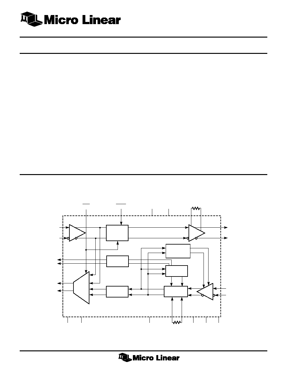
BLOCK DIAGRAM
1

ML6673
2
5
6
7
8
9
10
11
12
13
29
28
27
26
25
24
23
22
21
14 15 16 17 18 19 20
4
3
2
1
32 31 30
RXOUT+
RVCCD
SD≠
SD+
N/C
TGNDD
LPBK
TXOFF
N/C
RRSET1
RRSET2
N/C
N/C
RGND
N/C
N/C
TVCCA
TGNDA
TXIN+
TXIN≠
TVCCD
RTSET1
RTSET2
TPOUT+
TPOUT≠
RXOUT
≠
RVCCA
N/C
N/C
CMREF
TPIN+
TPIN≠
1
2
3
4
5
6
7
8
24
23
22
21
20
19
18
17
9
10
11
12
13
14
15
16
32
31
30
29
28
27
26
25
TPOUT≠
TPOUT+
RTSET2
RTSET1
TVCCD
TXIN≠
TXIN+
N/C
RRSET1
TPIN≠
TPIN+
CMREF
N/C
N/C
RVCCA
RXOUT≠
RXOUT+
RVCCD
SD≠
SD+
N/C
TGNDD
LPBK
TXOFF
RRSET2
N/C
N/C
RGND
N/C
N/C
TVCCA
TGNDA
ML6673
32-Pin PCC (Q32)
ML6673
32-Pin TQFP (H32-7)
PIN CONFIGURATION
NAME
FUNCTION
NAME
FUNCTION
TXIN+, TXIN≠
These differential ECL100K compatible
inputs receive NRZI data from the PHY
for transmission.
TPOUT+,
Outputs from the NRZI-MLT3 state
TPOUT≠
machine drive these differential current
outputs. The transmitter filter/transformer
module connects the media to these pins.
LPBK
This TTL input enables transmitter-
receiver loopback internally when
asserted low. When LPBK is asserted,
signal detect is asserted.
TXOFF
This TTL input forces the NRZI-MLT3
state machine to a high impedence state
when asserted low and shuts off transmit
bias current.
RTSET1,
An external 1% resistor connected
RTSET2
between these pins controls the
transmitter output current amplitude.
I
OUT
= 64 x 1.25V/RTSET
TVCCA,
Separate analog and digital transmitter
TVCCD
power supply pins help to isolate
sensitive circuitry from noise generating
digital functions. Both supplies are
nominally +5 volts.
PIN DESCRIPTION
TGNDA,
Analog and digital transmitter grounds
TGNDD
provide separate return paths for clean
and noisy signals.
SD+, SD≠
These differential ECL100K compatible
outputs indicate the presence of a data
signal with an amplitude exceeding a
preset threshold.
TPIN+, TPIN≠
MLT-3 encoded data from the receiver
filter/transformer module enters the
receiver through these pins.
RXOUT+,
Differential ECL100K compatible outputs
RXOUT≠
provide NRZI encoded data to the PHY.
RRSET1,
Internal time constants controlling the
RRSET2
equalizer's transfer function are set by an
external resistor connected across these
pins.
CMREF
This pin provides a DC common mode
reference point for the receiver inputs.
RVCCA,
Analog and digital supply pins are
RVCCD
separated to isolate clean and noisy
circuit functions. Both supplies are
nominally +5 volts.
RGND
Receiver ground.

ML6673
3
ELECTRICAL CHARACTERISTICS
Unless otherwise specified, T
A
= T
MIN
to T
MAX
, V
CC
= 5V
±
5%, RTSET = 2k
. (Note 1)
PARAMETER
CONDITIONS
MIN
TYP
MAX
UNITS
DC Characteristics
Supply Current
RVCCD
74
mA
RVCCA
65
mA
TVCCD
24
mA
TVCCA
6
mA
RVCCD + RVCCA + TVCCD + TVCCA
195
mA
TTL Inputs (TXOFF, LPBK)
V
IL
Input Low Voltage
0.8
V
V
IH
Input High Voltage
2.0
V
Differential Inputs (TPIN
±
, TXIN
±
)
TPIN+, TPIN≠
Common Mode Input Voltage
2.2
V
CC
V
TPIN+, TPIN≠
Differential Input Voltage
1.5
V
TPIN+, TPIN≠
Differential Input Resistance
10.0K
TPIN+, TPIN≠
Common Mode Input Current
+10
µ
A
TXIN+, TXIN≠
Input Voltage HIGH (V
IH
)
V
CC
≠1.165
V
CC
≠0.88
V
TXIN+, TXIN≠
Input Voltage LOW (V
IL
)
V
CC
≠1.810
V
CC
≠1.475
V
TXIN+, TXIN≠
Input Current LOW (I
IL
)
0.5
µ
A
TXIN+, TXIN≠
Input Current HIGH (I
IH
)
50
µ
A
Differential Outputs (SD
±
, RXOUT
±
, TPOUT
±
)
SD+, SD≠, RXOUT+, RXOUT≠
Output Voltage HIGH (V
OH
)
Note 3
V
CC
≠1.025
V
CC
≠0.88
V
SD+, SD≠, RXOUT+, RXOUT≠
Output Voltage LOW (V
OL
)
Note 3
V
CC
≠1.81
V
CC
≠1.62
V
ABSOLUTE MAXIMUM RATINGS
Absolute maximum ratings are those values beyond
which the device could be permanently damaged.
Absolute maximum ratings are stress ratings only and
functional device operation is not implied.
V
CC
Supply Voltage Range ................... GND ≠0.3V to 6V
Input Voltage Range
Digital Inputs ........................ GND ≠0.3V to V
CC
+0.3V
Output Current
TPOUT
±
, SD
±
, RXOUT
±
................................... 50mA
All other outputs ................................................. 10mA
Junction Temperature ............................................. 150
∞
C
Storage Temperature ................................ ≠65
∞
C to 150
∞
C
Lead Temperature (Soldering, 10 sec) ..................... 260
∞
C
Thermal Resistance (
JA
)
PLCC ............................................................... 60
∞
C/W
TQFP ............................................................... 80
∞
C/W
OPERATING CONDITIONS
V
CC
Supply Voltage ............................................ 5V
±
5%
T
A
, Ambient Temperature .............................. 0
∞
C to 70
∞
C
RTSET ............................................................... 2k
±
1%
RRSET .......................................................... 9.53k
±
1%
Receive Transformer Insertion Loss ..................... < ≠0.5dB

ML6673
4
ELECTRICAL CHARACTERISTICS
(Continued)
PARAMETER CONDITIONS MIN TYP MAX UNITS
Differential Outputs (SD
±
, RXOUT
±
, TPOUT
±
) (Continued)
TPOUT+, TPOUT≠
Output Current HIGH V
OUT
= V
CC
±
0.5, Note 2 38.0 42.0 mA
TPOUT+, TPOUT≠
Output Current LOW V
OUT
= V
CC
±
0.5, Note 2 0 0.5 mA
TPOUT+, TPOUT≠
Output Current Offset 0.5 mA
TPOUT+, TPOUT≠V
OUT
= V
CC
Output Amplitude Error Note 2 ≠5.0 5.0 %
TPOUT+, TPOUT≠V
OUT
= V
CC
±
1.1V
Output Voltage Compliance ≠2.0 +2.0 %
AC Characteristics
TPOUT+, TPOUT≠
Rise/Fall Time 2.0 ns
TPOUT+, TPOUT≠
Output Jitter 0.8 ns
RXOUT+, RXOUT≠
Rise/Fall Time 2.0 ns
RXOUT+, RXOUT≠
Output Jitter 2.0 ns
Note 1. Limits are guaranteed by 100% testing, sampling, or correlation with worst-case test conditions.
Note 2. Output current amplitude is determined by I
OUT
= 64 x 1.25V/RTSET.
Note 3. Output voltage levels are specified when terminated by 50
to V
CC
≠ 2V or equivalent load.
ML6673
5
FUNCTIONAL DESCRIPTION
The ML6673 MLT-3 transceiver is a physical media
dependent transceiver that allows the transmission and
reception of 125 Mbaud data over shielded twisted pair
cable or category 5 unshielded twisted pair cable. It
provides a standard Physical Media Dependent (PMD)
interface compatible with many FDDI chip sets.
The transmit section accepts NRZI data, converting it to a
three level MLT-3 code and sending the information on a
two pin current driven transmitter. The transmitted output
passes through an external low pass filter and transformer
before entering the connectors to the STP or UTP cable.
The output amplitude of the transmitted signal is
programmable through the external RTSET resistor.
I
V
RTSET
OUT
=
◊
64 1 25
.
For 100BASE-TX UTP application, the transmit amplitude
is 2VP-P differential achieved by setting RTSET = 2k
(1%).
The receive section accepts MLT-3 coded data after
passing through an isolation transformer and band
limiting filter. Before the data can be converted from MLT-
3 back to NRZI, the adaptive equalizer is used to
compensate for the amplitude and phase distortion
incurred from the cable. The adaptive control section
determines the signal amplitude (and therefore the cable
length) and adjusts the equalizer accordingly.
The receiver also includes the Baseline Wander correction
circuitry. The circuit will compensate and track the DC
baseline wander caused by DC imbalance of the received
data. It will tolerate the test pattern as specified in the
ANSI X3T12 TP-PMD specification. A parallel 10pF
capacitor can be connected between TPIN+ and TPIN≠
to improve Bit Error Rate.
The adaptive control block governs both the equalization
level as well as the signal detection status. Signal detect is
asserted when the equalizer control loop settles or when
loop back is asserted. When the input signal is small, the
equalization will be at its maximum.
After the signal has been equalized, it passes into the MLT-3
to NRZI converter where it is converted back to NRZI
and fed through the loopback multiplexer onto the
RXOUT± pins.
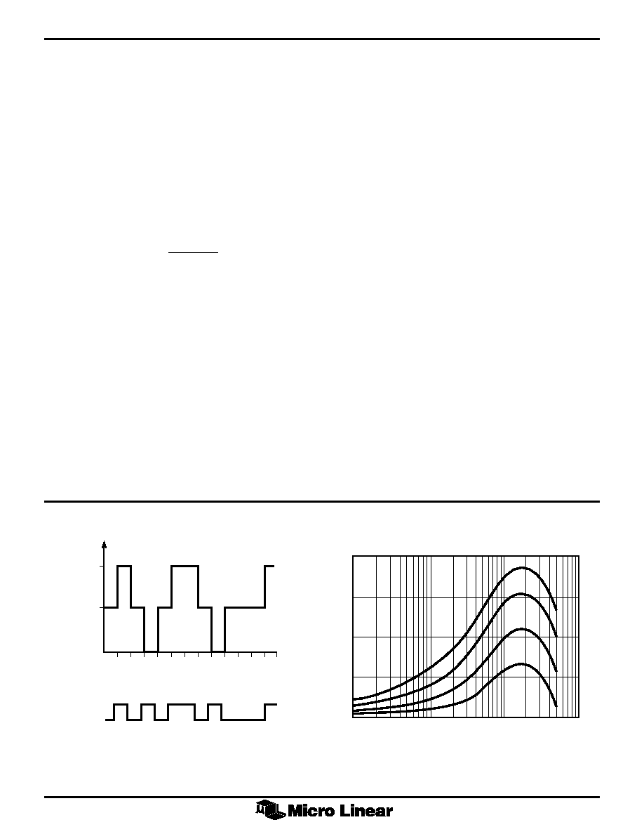
Figure 1 shows a timing diagram of NRZI data and the
equivalent MLT-3 data. The MLT-3 data shows the output
current I
OUT
for one side of the transmitter, either TPOUT+
or TPOUT≠. The other transmit output pin will be the
complement. Whenever there is a change in level in
NRZI, MLT-3 will change levels too. The maximum
fundamental frequency of MLT-3 is half of the maximum
fundamental of NRZI.
Figure 2 shows a typical gain vs frequency plot of the
adaptive equalizer for 0, 25, 50, 75 and 100 meter
category 5 cable lengths.
ML6671 COMPATIBILITY
The ML6673 implements the Baseline Wander correction
circuit, in addition to providing the functionality of the
existing ML6671 device. The ML6673 is plug-compatible
with the ML6671 with the following note:
∑ In the ML6673 design, the following passive
components may be eliminated
-- RSET resistor
-- RTH resistor
-- CAP1 capacitor
-- CAP2 capacitor
MLT-3 DATA
CURRENT (mA)
IOUT
IOUT/2
0
(nsec)
8 16 24 32 40 48 56 64 72 80 88 96
NRZI DATA
1
0
104
20
15
10
5
0
1 x 10⁶
1 x 10⁷
1 x 10⁸
1 x 10⁹
Figure 1. MLT-3 Encoding
Figure 2. Equalization Range