 | –≠–ª–µ–∫—Ç—Ä–æ–Ω–Ω—ã–π –∫–æ–º–ø–æ–Ω–µ–Ω—Ç: 24C04AT | –°–∫–∞—á–∞—Ç—å:  PDF PDF  ZIP ZIP |

©
1998 Microchip Technology Inc.
DS11183E-page 1
24C04A
FEATURES
∑ Low power CMOS technology
∑ Hardware write protect
∑ Two wire serial interface bus, I
2
CTM compatible
∑ 5.0V only operation
∑ Self-timed write cycle (including auto-erase)
∑ Page-write buffer
∑ 1 ms write cycle time for single byte
∑ 1,000,000 Erase/Write cycles guaranteed
∑ Data retention >200 years
∑ 8-pin DIP/SOIC packages
∑ Available for extended temperature ranges
DESCRIPTION
The Microchip Technology Inc. 24C04A is a 4K bit
Electrically Erasable PROM. The device is organized
as with a standard two wire serial interface. Advanced
CMOS technology allows a significant reduction in
power over NMOS serial devices. A special feature
provides hardware write protection for the upper half of
the block. The 24C04A has a page write capability of
up to eight bytes, and up to four 24C04A devices may
be connected to the same two wire bus.
This device offers fast (1ms) byte write and
extended (-40
∞
C to 125
∞
C) temperature operation.
It is recommended that all other applications use
Microchip's 24LC04B.
- Commercial (C):
0∞C to
+70∞C
- Industrial (I):
-40∞C to
+85∞C
- Automotive (E):
-40∞C to +125∞C
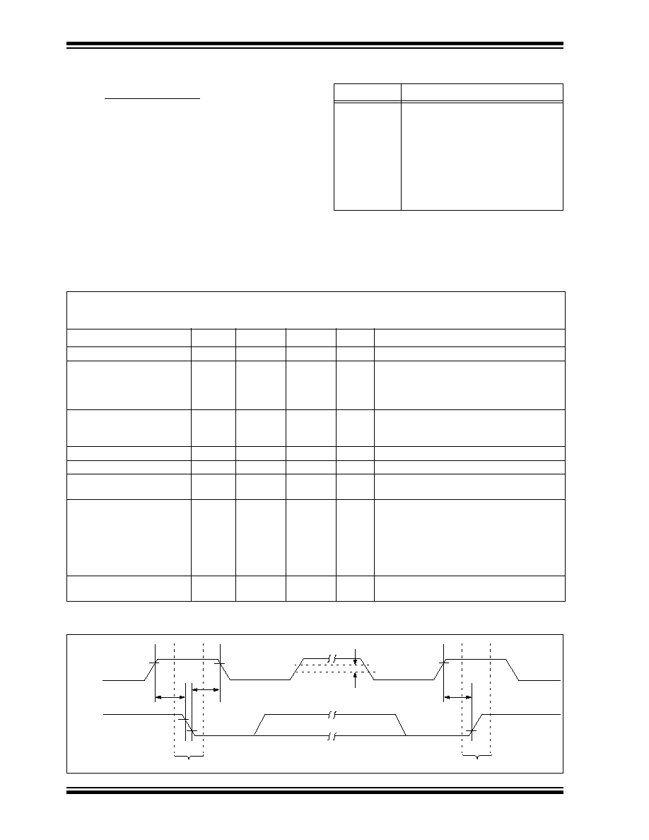
PACKAGE TYPES
BLOCK DIAGRAM
24C04A
24C04A
A0
A1
A2
V
SS
1
2
3
4
8
7
6
5
V
CC
WP
SCL
SDA
A0
A1
A2
V
SS
1
2
3
4
8
7
6
5
V
CC
WP
SCL
SDA
DIP
8-lead
SOIC
14-lead
SOIC
24C04A
SDA
NC
Vcc
WP
NC
SCL
NC
Vss
NC
A0
A1
NC
A2
NC
1
2
3
4
5
6
7
14
13
12
11
10
9
8
Vcc
Vss
SDA
SCL
Data
Buffer
(FIFO)
Data Reg.
V
PP
R/W Amp
Memory
Array
A
d
d
r
e
s
s
P
o
i
n
t
e
r
A0 to
A7
Increment
A8
Slave Addr.
Control
Logic
A0 A1 A2 WP
4K 5.0V I
2
C
TM
Serial EEPROM
I
2
C is a trademark of Philips Corporation.
24C04A
DS11183E-page 2
©
1998 Microchip Technology Inc.
1.0
ELECTRICAL CHARACTERISTICS
1.1
Maximum Ratings*
V
CC
...................................................................................7.0V
All inputs and outputs w.r.t. V
SS
............... -0.6V to V
CC
+1.0V
Storage temperature ..................................... -65∞C to +150∞C
Ambient temp. with power applied................. -65∞C to +125∞C
Soldering temperature of leads (10 seconds) ............. +300∞C
ESD protection on all pins................................................4 kV
*Notice:
Stresses above those listed under "Maximum ratings"
may cause permanent damage to the device. This is a stress rat-
ing only and functional operation of the device at those or any
other conditions above those indicated in the operational listings
of this specification is not implied. Exposure to maximum rating
conditions for extended periods may affect device reliability.
TABLE 1-1:
PIN FUNCTION TABLE
Name
Function
A0
No Function - Must be connected to
V
CC
or V
SS
A1, A2
Chip Address Inputs
V
SS
Ground
SDA
Serial Address/Data I/O
SCL
Serial Clock
WP
Write Protect Input
V
CC
+5V Power Supply
TABLE 1-2:
DC CHARACTERISTICS
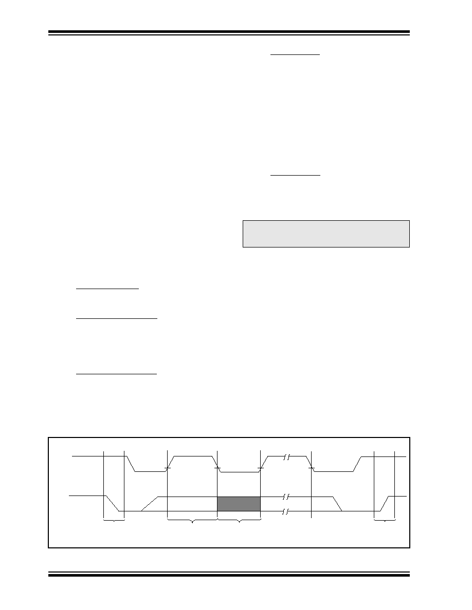
FIGURE 1-1:
BUS TIMING START/STOP
V
CC
= +5V (
±
10%)
Commercial (C): Tamb = 0
∞
C to +70
∞
C
Industrial (I):
Tamb = -40
∞
C to +85
∞
C
Automotive (E):
Tamb = -40
∞
C to +125
∞
C
Parameter
Symbol
Min.
Max.
Units
Conditions
V
CC
detector threshold
V
TH
2.8
4.5
V
SCL and SDA pins:
High level input voltage
Low level input voltage
Low level output voltage
V
IH
V
IL
V
OL
V
CC
x 0.7
-0.3
V
CC
+ 1
V
CC
x 0.3
0.4
V
V
V
I
OL
= 3.2 mA (SDA only)
A1 & A2 pins:
High level input voltage
Low level input voltage
V
IH
V
IL
V
CC
- 0.5
-0.3
V
CC
+ 0.5
0.5
V
V
Input leakage current
I
LI
--
10
µ
A
V
IN
= 0V to V
CC
Output leakage current
I
LO
--
10
µ
A
V
OUT
= 0V to V
CC
Pin capacitance
(all inputs/outputs)
C
IN
,
C
OUT
--
7.0
pF
V
IN
/V
OUT
= 0V (Note)
Tamb = +25∞C, f = 1 MHz
Operating current
I
CC
Write
--
3.5
mA
F
CLK
= 100 kHz, program cycle time = 1 ms,
Vcc = 5V, Tamb = 0∞C to +70∞C
I
CC
Write
--
4.25
mA
F
CLK
= 100 kHz, program cycle time = 1 ms,
Vcc = 5V, Tamb = (I) and (E)
I
CC
Read
--
750
µ
A
V
CC
= 5V, Tamb= (C), (I) and (E)
Standby current
I
CCS
--
100
µ
A
SDA=SCL=V
CC
=5V (no PROGRAM active)
WP/TEST = V
SS
, A0, A1, A2 = V
SS
Note: This parameter is periodically sampled and not 100% tested
T
SU
:
STA
T
HD
:
STA
V
HYS
T
SU
:
STO
START
STOP
SCL
SDA

©
1998 Microchip Technology Inc.
DS11183E-page 3
24C04A
TABLE 1-3:
AC CHARACTERISTICS
FIGURE 1-2:
BUS TIMING DATA
Parameter
Symbol
Min.
Typ
Max.
Units
Remarks
Clock frequency
F
CLK
--
--
100
kHz
Clock high time
T
HIGH
4000
--
--
ns
Clock low time
T
LOW
4700
--
--
ns
SDA and SCL rise time
T
R
--
--
1000
ns
SDA and SCL fall time
T
F
--
--
300
ns
START condition hold time
T
HD
:S
TA
4000
--
--
ns
After this period the first
clock pulse is generated
START condition setup time
T
SU
:S
TA
4700
--
--
ns
Only relevant for repeated
START condition
Data input hold time
T
HD
:D
AT
0
--
--
ns
Data input setup time
T
SU
:D
AT
250
--
--
ns
Data output delay time
T
AA
300
--
3500
(Note 1)
STOP condition setup time
T
SU
:S
TO
4700
--
--
ns
Bus free time
T
BUF
4700
--
--
ns
Time the bus must be free
before a new transmission
can start
Input filter time constant
(SDA and SCL pins)
T
I
--
--
100
ns
Program cycle time
T
WC
--
.4
1
ms
Byte mode
.4N
N
ms
Page mode, N=# of bytes
Endurance
--
1M
--
--
cycles
25
∞
C, Vcc = 5.0V, Block
Mode (Note 2)
Note 1: As transmitter the device must provide this internal minimum delay time to bridge the undefined region (min-
imum 300 ns) of the falling edge of SCL to avoid unintended generation of START or STOP conditions.
2: This parameter is not tested but guaranteed by characterization. For endurance estimates in a specific appli-
cation, please consult the Total Endurance Model which can be obtained on our website.
T
SU
:
STA
T
F
T
LOW
T
HIGH
T
R
T
HD
:
DAT
T
SU
:
DAT
T
SU
:
STO
T
HD
:
STA
T
BUF
T
AA
T
AA
T
SP
T
HD
:
STA
SCL
SDA
IN
SDA
OUT
24C04A
DS11183E-page 4
©
1998 Microchip Technology Inc.
2.0
FUNCTIONAL DESCRIPTION
The 24C04A supports a bidirectional two wire bus and
data transmission protocol. A device that sends data
onto the bus is defined as transmitter, and a device
receiving data as receiver. The bus has to be con-
trolled by a master device which generates the serial
clock (SCL), controls the bus access, and generates
the START and STOP conditions, while the 24C04A
works as slave. Both master and slave can operate as
transmitter or receiver but the master device deter-
mines which mode is activated.
Up to four 24C04As can be connected to the bus,
selected by A1 and A2 chip address inputs. A0 must
be tied to V
CC
or V
SS
.
3.0
BUS CHARACTERISTICS
The following bus protocol has been defined:
∑ Data transfer may be initiated only when the bus
is not busy.
∑ During data transfer, the data line must remain
stable whenever the clock line is HIGH. Changes
in the data line while the clock line is HIGH will be
interpreted as a START or STOP condition.
Accordingly, the following bus conditions have been
defined (Figure 3-1).
3.1
Bus not Busy (A)
Both data and clock lines remain HIGH.
3.2
Start Data Transfer (B)
A HIGH to LOW transition of the SDA line while the
clock (SCL) is HIGH determines a START condition.
All commands must be preceded by a START condi-
tion.
3.3
Stop Data Transfer (C)
A LOW to HIGH transition of the SDA line while the
clock (SCL) is HIGH determines a STOP condition. All
operations must be ended with a STOP condition.
3.4
Data Valid (D)
The state of the data line represents valid data when,
after a START condition, the data line is stable for the
duration of the HIGH period of the clock signal.
The data on the line must be changed during the LOW
period of the clock signal. There is one clock pulse per
bit of data.
Each data transfer is initiated with a START condition
and terminated with a STOP condition. The number of
the data bytes transferred between the START and
STOP conditions is determined by the master device
and is theoretically unlimited.
3.5
Acknowledge
Each receiving device, when addressed, is obliged to
generate an acknowledge after the reception of each
byte. The master device must generate an extra clock
pulse which is associated with this acknowledge bit.
The device that acknowledges has to pull down the
SDA line during the acknowledge clock pulse in such a
way that the SDA line is stable LOW during the HIGH
period of the acknowledge related clock pulse. Of
course, setup and hold times must be taken into
account. A master must signal an end of data to the
slave by not generating an acknowledge bit on the last
byte that has been clocked out of the slave. In this
case, the slave must leave the data line HIGH to enable
the master to generate the STOP condition.
Note:
The 24C04A does not generate any
acknowledge bits if an internal program-
ming cycle is in progress.
FIGURE 3-1:
DATA TRANSFER SEQUENCE ON THE SERIAL BUS
SCL
SDA
(A)
(B)
(D)
(D)
(A)
(C)
START
CONDITION
ADDRESS OR
ACKNOWLEDGE
VALID
DATA
ALLOWED
TO CHANGE
STOP
CONDITION

©
1998 Microchip Technology Inc.
DS11183E-page 5
24C04A
4.0
SLAVE ADDRESS
The chip address inputs A1 and A2 must be externally
connected to either V
CC
or ground (V
SS
), thereby
assigning a unique address to each device. A0 is not
used on the 24C04A and must be connected to either
V
CC
or V
SS
. Up to four 24C04A devices may be con-
nected to the bus. Chip selection is then accomplished
through software by setting the bits A1 and A2 of the
slave address to the corresponding hard-wired logic lev-
els of the selected 24C04A. After generating a START
condition, the bus master transmits the slave address
consisting of a 4-bit device code (1010), followed by the
chip address bits A0, A1 and A2. The seventh bit of that
byte (A0) is used to select the upper block (addresses
100--1FF) or the lower block (addresses 000--0FF) of
the array.
The eighth bit of the slave address determines if the
master device wants to read or write to the 24C04A
(Figure 4-1).
The 24C04A monitors the bus for its corresponding
slave address all the time. It generates an acknowl-
edge bit if the slave address was true and it is not in a
programming mode.
FIGURE 4-1:
SLAVE ADDRESS
ALLOCATION
SLAVE ADDRESS
1
0
1
0
A2
A1
A0
R/W
A
START
READ/WRITE
5.0
BYTE PROGRAM MODE
In this mode, the master sends addresses and one
data byte to the 24C04A.
Following the START signal from the master, the device
code (4-bits), the slave address (3-bits), and the R/W
bit, which is logic LOW, are placed onto the bus by the
master. This indicates to the addressed 24C04A that a
byte with a word address will follow after it has gener-
ated an acknowledge bit. Therefore the next byte trans-
mitted by the master is the word address and will be
written into the address pointer of the 24C04A. After
receiving the acknowledge, the master device trans-
mits the data word to be written into the addressed
memory location. The 24C04A acknowledges again
and the master generates a STOP condition. This ini-
tiates the internal programming cycle (Figure 6-1).
24C04A
DS11183E-page 6
©
1998 Microchip Technology Inc.
6.0
PAGE PROGRAM MODE
To program the master sends addresses and data to
the 24C04A which is the slave (Figure
6-1 and
Figure 6-2). This is done by supplying a START condi-
tion followed by the 4-bit device code, the 3-bit slave
address, and the R/W bit which is defined as a logic
LOW for a write. This indicates to the addressed slave
that a word address will follow so the slave outputs the
acknowledge pulse to the master during the ninth clock
pulse. When the word address is received by the
24C04A, it places it in the lower 8 bits of the address
pointer defining which memory location is to be written.
(The A0 bit transmitted with the slave address is the
ninth bit of the address pointer). The 24C04A will gen-
erate an acknowledge after every 8-bits received and
store them consecutively in a RAM (8 bytes maximum)
buffer until a STOP condition is detected. This STOP
condition initiates the internal programming cycle.. If
more than 8 bytes are transmitted by the master, the
24C04A will roll over and overwrite the data beginning
with the first received byte. This does not affect erase/
write cycles of the EEPROM array and is accomplished
as a result of only allowing the address registers bot-
tom 3 bits to increment while the upper 5 bits remain
unchanged.
If the master generates a STOP condition after trans-
mitting the first data word (Point `P' on Figure 6-1), byte
programming mode is entered.
The internal, completely self-timed PROGRAM cycle
starts after the STOP condition has been generated by
the master and all received data bytes in the page
buffer will be written in a serial manner.
The PROGRAM cycle takes N milliseconds, whereby N
is the number of received data bytes.
FIGURE 6-1:
BYTE WRITE
FIGURE 6-2:
PAGE WRITE
S
P
BUS ACTIVITY
MASTER
SDA LINE
BUS ACTIVITY
S
T
A
R
T
S
T
O
P
CONTROL
BYTE
WORD
ADDRESS
DATA
A
C
K
A
C
K
A
C
K
S
P
BUS ACTIVITY
MASTER
SDA LINE
BUS ACTIVITY
S
T
A
R
T
CONTROL
BYTE
WORD
ADDRESS (n)
DATA n
DATA n + 7
S
T
O
P
A
C
K
A
C
K
A
C
K
A
C
K
A
C
K
DATA n + 1

©
1998 Microchip Technology Inc.
DS11183E-page 7
24C04A
7.0
ACKNOWLEDGE POLLING
Since the device will not acknowledge during a write
cycle, this can be used to determine when the cycle is
complete (this feature can be used to maximize bus
throughput). Once the stop condition for a write com-
mand has been issued from the master, the device ini-
tiates the internally timed write cycle. ACK polling can
be initiated immediately. This involves the master send-
ing a start condition followed by the control byte for a
write command (R/W = 0). If the device is still busy with
the write cycle, then no ACK will be returned. If the
cycle is complete, then the device will return the ACK
and the master can then proceed with the next read or
write command. See Figure 7-1 for flow diagram.
FIGURE 7-1:
ACKNOWLEDGE POLLING
FLOW
Send
Write Command
Send Stop
Condition to
Initiate Write Cycle
Send Start
Send Control Byte
with R/W = 0
Did Device
Acknowledge
(ACK = 0)?
Next
Operation
NO
YES
8.0
WRITE PROTECTION
Programming of the upper half of the memory will not
take place if the WP pin is connected to V
CC
(+5.0V).
The device will accept slave and word addresses but if
the memory accessed is write protected by the WP pin,
the 24C04A will not generate an acknowledge after the
first byte of data has been received, and thus the pro-
gram cycle will not be started when the STOP condition
is asserted.

24C04A
DS11183E-page 8
©
1998 Microchip Technology Inc.
FIGURE 9-1:
CURRENT ADDRESS READ
FIGURE 9-2:
RANDOM READ
FIGURE 9-3:
SEQUENTIAL READ
S
P
BUS ACTIVITY
MASTER
SDA LINE
BUS ACTIVITY
S
T
A
R
T
S
T
O
P
CONTROL
BYTE
DATA n
A
C
K
N
O
A
C
K
S
P
S
BUS ACTIVITY
MASTER
SDA LINE
BUS ACTIVITY
S
T
A
R
T
S
T
O
P
CONTROL
BYTE
A
C
K
WORD
ADDRESS (n)
CONTROL
BYTE
S
T
A
R
T
DATA (n)
A
C
K
A
C
K
N
O
A
C
K
P
BUS ACTIVITY
MASTER
SDA LINE
BUS ACTIVITY
S
T
O
P
CONTROL
BYTE
A
C
K
N
O
A
C
K
DATA n
DATA n + 1
DATA n + 2
DATA n + X
A
C
K
A
C
K
A
C
K
9.0
READ MODE
In this mode the 24C04A transmits data to the master
devide.
As can be seen from Figure 9-2 and Figure 9-3, the
master first sets up the slave and word addresses by
doing a write. (Note: Although this is a read mode, the
address pointer must be written to). During this period
the 24C04A generates the necessary acknowledge
bits as defined in the appropriate section.
The master now generates another START condition
and transmits the slave address again, except this time
the read/write bit is set into the read mode. After the
slave generates the acknowledge bit, it then outputs
the data from the addressed location on to the SDA pin,
increments the address pointer and, if it receives an
acknowledge from the master, will transmit the next
consecutive byte. This auto-increment sequence is
only aborted when the master sends a STOP condition
instead of an acknowledge.
Note 1: If the master knows where the address
pointer is, it can begin the read sequence
at the current address (Figure 9-1) and
save time transmitting the slave and word
addresses.
Note 2: In all modes, the address pointer will not
increment through a block (256 byte)
boundary, but will rotate back to the first
location in that block.

©
1998 Microchip Technology Inc.
DS11183E-page 9
24C04A
10.0
PIN DESCRIPTION
10.1
A0, A1, A2 Chip Address Inputs
A0 is not used as a chip select bit and must be tied to
either Vss or Vcc. The levels on the remaining two
address inputs(A1, A2) are compared with the corre-
sponding bits in the slave address. The chip is selected
if the compare is true. These inputs must be connected
to either V
SS
or V
CC
.
These two address inputs allow up to four 24C04A's
can be connected to the bus
10.2
SDA Serial Address/Data Input/Output
This is a bidirectional pin used to transfer addresses
and data into and data out of the device. It is an open
drain terminal, therefore the SDA bus requires a pull-up
resistor to V
CC
(typical 10K
).
For normal data transfer, SDA is allowed to change only
during SCL LOW. Changes during SCL HIGH are
reserved for indicating the START and STOP condi-
tions.
10.3
SCL Serial Clock
This input is used to synchronize the data transfer from
and to the device.
10.4
WP Write Protection
This pin must be connected to either V
CC
or V
SS
. If tied
to V
CC
, write operations to the upper memory block will
not be executed. Read operations are possible.
If tied to V
SS
, normal memory operation is enabled
(read/write the entire memory).
This feature allows the user to assign the upper half of
the memory as ROM which can be protected against
accidental programming. When write is disabled, slave
address and word address will be acknowledged but
data will not be acknowledged.
Note 1: A "page" is defined as the maximum num-
ber of bytes that can be programmed in a
single write cycle. The 24C04A page is 8
bytes long.
Note 2: A "block" is defined as a continuous area
of memory with distinct boundaries. The
address pointer can not cross the bound-
ary from one block to another. It will how-
ever, wrap around from the end of a block
to the first location in the same block. The
24C04A has two blocks, 256 bytes each.

24C04A
DS11183E-page 10
©
1998 Microchip Technology Inc.
NOTES:

24C04A
24C04A Product Identification System
To order or to obtain information, e.g., on pricing or delivery, please use the listed part numbers, and refer to the factory or the listed
sales offices.
Sales and Support
Data Sheets
Products supported by a preliminary Data Sheet may have an errata sheet describing minor operational differences and recom-
mended workarounds. To determine if an errata sheet exists for a particular device, please contact one of the following:
1.
Your local Microchip sales office
2.
The Microchip Corporate Literature Center U.S. FAX: (602) 786-7277
3.
The Microchip Worldwide Web Site (www.microchip.com)
Package:
P = Plastic DIP
SN = Plastic SOIC (150 mil Body), 8-lead
SM = Plastic SOIC (207 mil Body), 8-lead
SL = Plastic SOIC (150 mil Body), 14-lead
Temperature
Range:
Blank = 0
∞
C to +70
∞
C
= -40
∞
C to +85
∞
C
E = -40
∞
C to +125
∞
C
Device:
24C04A
4K I
2
C Serial EEPROM
24C04AT
4K I
2
C Serial EEPROM (Tape and Reel)
24C04A
-
/P
DS11183E-page 11
©
1998 Microchip Technology Inc.

Information contained in this publication regarding device applications and the like is intended for suggestion only and may be superseded by updates. No representation or warranty is given and no liability is assumed
by Microchip Technology Incorporated with respect to the accuracy or use of such information, or infringement of patents or other intellectual property rights arising from such use or otherwise. Use of Microchip's products
as critical components in life support systems is not authorized except with express written approval by Microchip. No licenses are conveyed, implicitly or otherwise, under any intellectual property rights. The Microchip
logo and name are registered trademarks of Microchip Technology Inc. in the U.S.A. and other countries. All rights reserved. All other trademarks mentioned herein are the property of their respective companies.
1999 Microchip Technology Inc.
All rights reserved. © 1999 Microchip Technology Incorporated. Printed in the USA. 11/99
Printed on recycled paper.
AMERICAS
Corporate Office
Microchip Technology Inc.
2355 West Chandler Blvd.
Chandler, AZ 85224-6199
Tel: 480-786-7200 Fax: 480-786-7277
Technical Support: 480-786-7627
Web Address: http://www.microchip.com
Atlanta
Microchip Technology Inc.
500 Sugar Mill Road, Suite 200B
Atlanta, GA 30350
Tel: 770-640-0034 Fax: 770-640-0307
Boston
Microchip Technology Inc.
5 Mount Royal Avenue
Marlborough, MA 01752
Tel: 508-480-9990 Fax: 508-480-8575
Chicago
Microchip Technology Inc.
333 Pierce Road, Suite 180
Itasca, IL 60143
Tel: 630-285-0071 Fax: 630-285-0075
Dallas
Microchip Technology Inc.
4570 Westgrove Drive, Suite 160
Addison, TX 75248
Tel: 972-818-7423 Fax: 972-818-2924
Dayton
Microchip Technology Inc.
Two Prestige Place, Suite 150
Miamisburg, OH 45342
Tel: 937-291-1654 Fax: 937-291-9175
Detroit
Microchip Technology Inc.
Tri-Atria Office Building
32255 Northwestern Highway, Suite 190
Farmington Hills, MI 48334
Tel: 248-538-2250 Fax: 248-538-2260
Los Angeles
Microchip Technology Inc.
18201 Von Karman, Suite 1090
Irvine, CA 92612
Tel: 949-263-1888 Fax: 949-263-1338
New York
Microchip Technology Inc.
150 Motor Parkway, Suite 202
Hauppauge, NY 11788
Tel: 631-273-5305 Fax: 631-273-5335
San Jose
Microchip Technology Inc.
2107 North First Street, Suite 590
San Jose, CA 95131
Tel: 408-436-7950 Fax: 408-436-7955
AMERICAS
(continued)
Toronto
Microchip Technology Inc.
5925 Airport Road, Suite 200
Mississauga, Ontario L4V 1W1, Canada
Tel: 905-405-6279 Fax: 905-405-6253
ASIA/PACIFIC
Hong Kong
Microchip Asia Pacific
Unit 2101, Tower 2
Metroplaza
223 Hing Fong Road
Kwai Fong, N.T., Hong Kong
Tel: 852-2-401-1200 Fax: 852-2-401-3431
Beijing
Microchip Technology, Beijing
Unit 915, 6 Chaoyangmen Bei Dajie
Dong Erhuan Road, Dongcheng District
New China Hong Kong Manhattan Building
Beijing 100027 PRC
Tel: 86-10-85282100 Fax: 86-10-85282104
India
Microchip Technology Inc.
India Liaison Office
No. 6, Legacy, Convent Road
Bangalore 560 025, India
Tel: 91-80-229-0061 Fax: 91-80-229-0062
Japan
Microchip Technology Intl. Inc.
Benex S-1 6F
3-18-20, Shinyokohama
Kohoku-Ku, Yokohama-shi
Kanagawa 222-0033 Japan
Tel: 81-45-471- 6166 Fax: 81-45-471-6122
Korea
Microchip Technology Korea
168-1, Youngbo Bldg. 3 Floor
Samsung-Dong, Kangnam-Ku
Seoul, Korea
Tel: 82-2-554-7200 Fax: 82-2-558-5934
Shanghai
Microchip Technology
RM 406 Shanghai Golden Bridge Bldg.
2077 Yan'an Road West, Hong Qiao District
Shanghai, PRC 200335
Tel: 86-21-6275-5700 Fax: 86 21-6275-5060
ASIA/PACIFIC
(continued)
Singapore
Microchip Technology Singapore Pte Ltd.
200 Middle Road
#07-02 Prime Centre
Singapore 188980
Tel: 65-334-8870 Fax: 65-334-8850
Taiwan, R.O.C
Microchip Technology Taiwan
10F-1C 207
Tung Hua North Road
Taipei, Taiwan, ROC
Tel: 886-2-2717-7175 Fax: 886-2-2545-0139
EUROPE
United Kingdom
Arizona Microchip Technology Ltd.
505 Eskdale Road
Winnersh Triangle
Wokingham
Berkshire, England RG41 5TU
Tel: 44 118 921 5858 Fax: 44-118 921-5835
Denmark
Microchip Technology Denmark ApS
Regus Business Centre
Lautrup hoj 1-3
Ballerup DK-2750 Denmark
Tel: 45 4420 9895 Fax: 45 4420 9910
France
Arizona Microchip Technology SARL
Parc d'Activite du Moulin de Massy
43 Rue du Saule Trapu
Batiment A - ler Etage
91300 Massy, France
Tel: 33-1-69-53-63-20 Fax: 33-1-69-30-90-79
Germany
Arizona Microchip Technology GmbH
Gustav-Heinemann-Ring 125
D-81739 M¸nchen, Germany
Tel: 49-89-627-144 0 Fax: 49-89-627-144-44
Italy
Arizona Microchip Technology SRL
Centro Direzionale Colleoni
Palazzo Taurus 1 V. Le Colleoni 1
20041 Agrate Brianza
Milan, Italy
Tel: 39-039-65791-1 Fax: 39-039-6899883
11/15/99
W
ORLDWIDE
S
ALES
AND
S
ERVICE
Microchip received QS-9000 quality system
certification for its worldwide headquarters,
design and wafer fabrication facilities in
Chandler and Tempe, Arizona in July 1999. The
Company's quality system processes and
procedures are QS-9000 compliant for its
PICmicro
Æ
8-bit MCUs, K
EE
L
OQ
Æ
code hopping
devices, Serial EEPROMs and microperipheral
products. In addition, Microchip's quality
system for the design and manufacture of
development systems is ISO 9001 certified.