2002 Microchip Technology Inc.
DS21705A-page 1
M
MCP73826
Features
· Linear Charge Management Controller for Single
Lithium-Ion Cells
· High Accuracy Preset Voltage Regulation:
+1% (max)
· Two Preset Voltage Regulation Options:
- 4.1V - MCP73826-4.1
- 4.2V - MCP73826-4.2
· Programmable Charge Current
· Automatic Cell Preconditioning of Deeply
Depleted Cells, Minimizing Heat Dissipation Dur-
ing Initial Charge Cycle
· Automatic Power-Down when Input Power
Removed
· Temperature Range: -20°C to +85°C
· Packaging: 6-Pin SOT-23A
Applications
· Single Cell Lithium-Ion Battery Chargers
· Personal Data Assistants
· Cellular Telephones
· Hand Held Instruments
· Cradle Chargers
· Digital Cameras
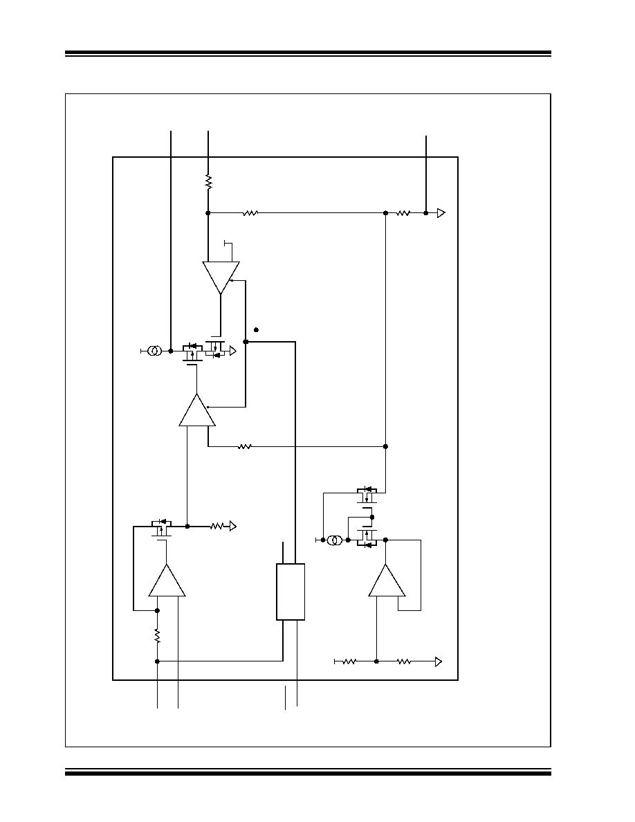
Typical Application Circuit
Description
The MCP73826 is a linear charge management con-
troller for use in space-limited, cost sensitive applica-
tions. The MCP73826 combines high accuracy
constant voltage, controlled current regulation, and cell
preconditioning in a space saving 6-pin SOT-23A pack-
age. The MCP73826 provides a stand-alone charge
management solution.
The MCP73826 charges the battery in three phases:
preconditioning, controlled current, and constant volt-
age. If the battery voltage is below the internal low-volt-
age threshold, the battery is preconditioned with a
foldback current. The preconditioning phase protects
the lithium-ion cell and minimizes heat dissipation.
Following the preconditioning phase, the MCP73826
enters the controlled current phase. The MCP73826
allows for design flexibility with a programmable charge
current set by an external sense resistor. The charge
current is ramped up, based on the cell voltage, from
the foldback current to the peak charge current estab-
lished by the sense resistor. This phase is maintained
until the battery reaches the charge-regulation voltage.
Then, the MCP73826 enters the final phase, constant
voltage. The accuracy of the voltage regulation is better
than ±1% over the entire operating temperature range
and supply voltage range. The MCP73826-4.1 is preset
to a regulation voltage of 4.1V, while the MCP73826-
4.2 is preset to 4.2V.
The MCP73826 operates with an input voltage range
from 4.5V to 5.5V. The MCP73826 is fully specified
over the ambient temperature range of -20°C to +85°C.
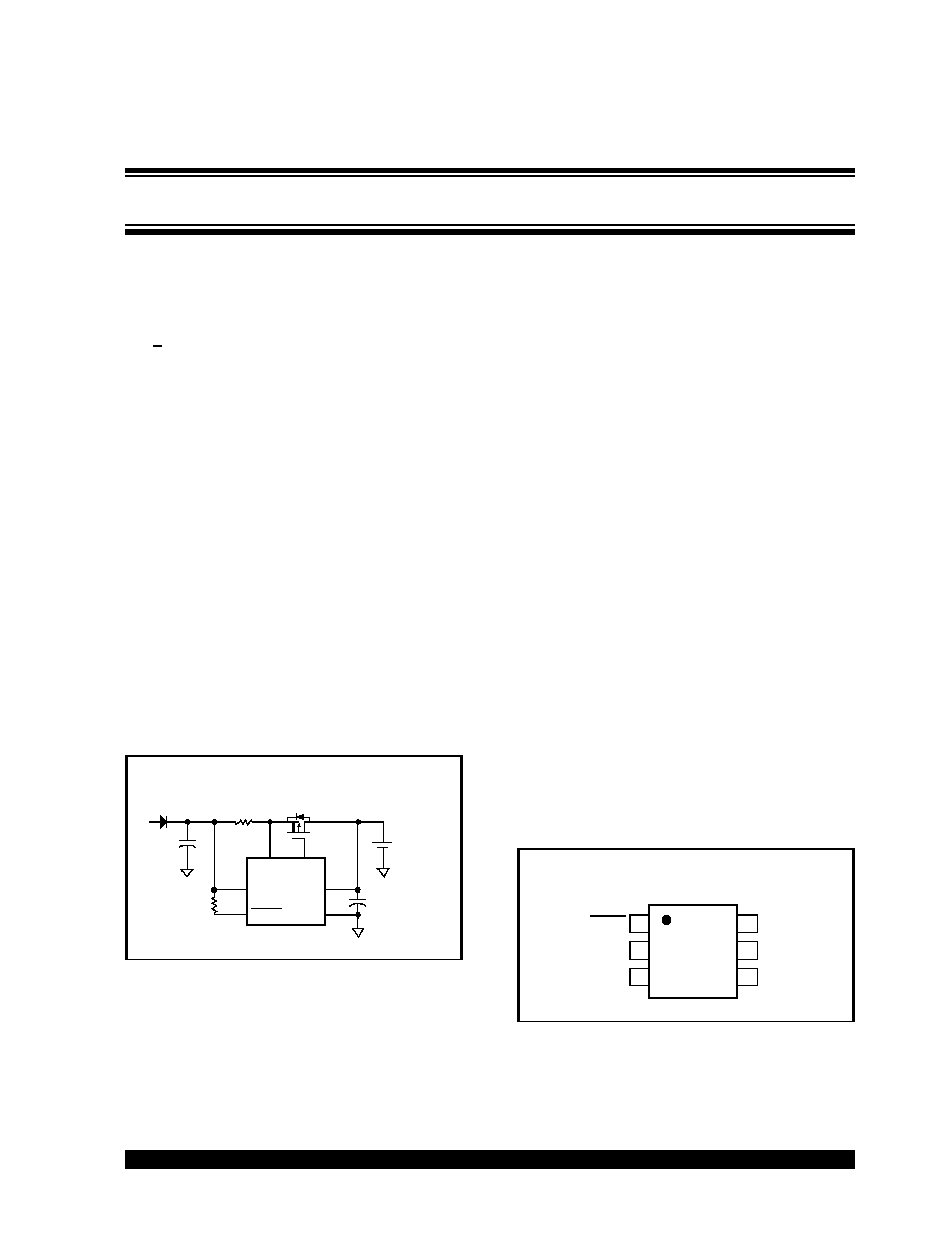
Package Type
+
-
GND
V
DRV
V
SNS
V
IN
V
BAT
SHDN
1
2
3
6
5
4
10 µF
100 k
100 m
V
IN
Single
Lithium-Ion
Cell
NDS8434
MA2Q705
500 mA Lithium-Ion Battery Charger
5V
10 µF
MCP73826
6-Pin SOT-23A
GND
V
DRV
V
SNS
V
IN
V
BAT
SHDN 1
2
3
6
5
MCP73826
4
Single Cell Lithium-Ion Charge Management Controller
2002 Microchip Technology Inc.
DS21705A-page 3
MCP73826
1.0
ELECTRICAL
CHARACTERISTICS
1.1
Maximum Ratings*
V
IN
................................................................................... -0.3V to 6.0V
All inputs and outputs w.r.t. GND ................-0.3 to (V
IN
+0.3)V
Current at V
DRV
.......................................................... +/-1 mA
Maximum Junction Temperature, T
J
.............................. 150°C
Storage temperature .....................................-65°C to +150°C
ESD protection on all pins
..................................................
4 kV
*Notice: Stresses above those listed under "Maximum Ratings" may
cause permanent damage to the device. This is a stress rating only and
functional operation of the device at those or any other conditions
above those indicated in the operational listings of this specification is
not implied. Exposure to maximum rating conditions for extended peri-
ods may affect device reliability.
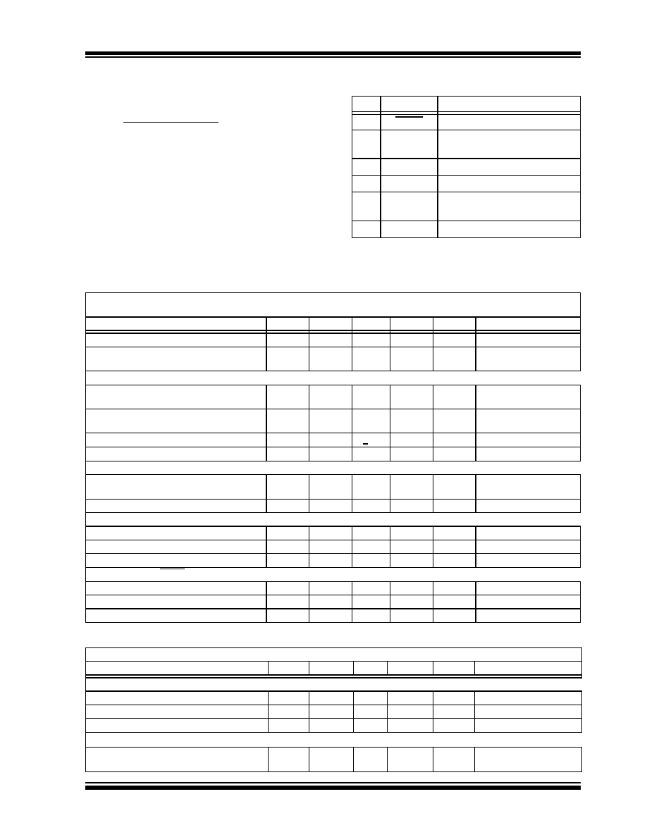
PIN FUNCTION TABLE
DC CHARACTERISTICS: MCP73826-4.1, MCP73826-4.2
TEMPERATURE SPECIFICATIONS
Pin
Name
Description
1
SHDN
Logic Shutdown
2
GND
Battery Management
0V Reference
3
V
BAT
Cell Voltage Monitor Input
4
V
DRV
Drive Output
5
V
IN
Battery Management
Input Supply
6
V
SNS
Charge Current Sense Input
Unless otherwise specified, all limits apply for V
IN
= [V
REG
(typ)+1V], R
SENSE
= 500 m
,
T
A
= -20°C to +85°C.
Typical values are at +25°C. Refer to Figure 1-1 for test circuit.
Parameter
Sym
Min
Typ
Max
Units
Conditions
Supply Voltage
V
IN
4.5
--
5.5
V
Supply Current
I
IN
--
--
0.5
260
15
560
µA
Shutdown, V
SHDN
= 0V
Constant Voltage Mode
Voltage Regulation (Constant Voltage Mode)
Regulated Output Voltage
V
REG
4.059
4.158
4.1
4.2
4.141
4.242
V
V
MCP73826-4.1 only
MCP73826-4.2 only
Line Regulation
V
BAT
-10
--
10
mV
V
IN
= 4.5V to 5.5V,
I
OUT
= 75 mA
Load Regulation
V
BAT
-1
+0.2
1
mV
I
OUT
= 10 mA to 75 mA
Output Reverse Leakage Current
I
LK
--
8
--
µA
V
IN
=Floating, V
BAT
=V
REG
External MOSFET Gate Drive
Gate Drive Current
I
DRV
--
0.08
--
--
1
--
mA
mA
Sink, CV Mode
Source, CV Mode
Gate Drive Minimum Voltage
V
DRV
--
1.6
--
V
Current Regulation (Controlled Current Mode)
Current Sense Gain
A
CS
--
100
--
dB
(V
SNS
-V
DRV
) /
V
BAT
Current Limit Threshold
V
CS
40
53
75
mV
(V
IN
-V
SNS
) at I
OUT
Foldback Current Scale Factor
K
--
0.43
--
A/A
Shutdown Input - SHDN
Input High Voltage Level
V
IH
40
--
--
%V
IN
Input Low Voltage Level
V
IL
--
--
25
%V
IN
Input Leakage Current
I
LK
--
--
1
µA
V
SHDN
= 0V to 5.5V
Unless otherwise specified, all limits apply for V
IN
= 4.5V-5.5V
Parameters
Sym
Min
Typ
Max
Units
Conditions
Temperature Ranges
Specified Temperature Range
T
A
-20
--
+85
°C
Operating Temperature Range
T
A
-40
--
+125
°C
Storage Temperature Range
T
A
-65
--
+150
°C
Thermal Package Resistances
Thermal Resistance, 6-Pin SOT-23A
JA
--
230
--
°C/W
4-Layer JC51-7 Standard
Board, Natural Convection
2002 Microchip Technology Inc.
DS21705A-page 5
MCP73826
2.0
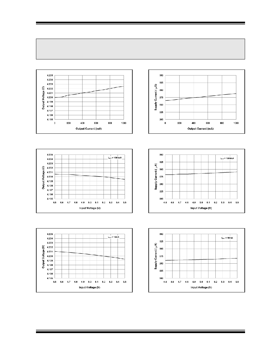
TYPICAL PERFORMANCE CHARACTERISTICS
Note: Unless otherwise indicated, I
OUT
= 10 mA, Constant Voltage Mode, T
A
= 25°C. Refer to Figure 1-1 for test circuit.
FIGURE 2-1:
Output Voltage vs. Output Current
(MCP73826-4.2).
FIGURE 2-2:
Output Voltage vs. Input Voltage
(MCP73826-4.2).
FIGURE 2-3:
Output Voltage vs. Input Voltage
(MCP73826-4.2).
FIGURE 2-4:
Supply Current vs. Output Current.
FIGURE 2-5:
Supply Current vs. Input Voltage.
FIGURE 2-6:
Supply Current vs. Input Voltage.
Note:
The graphs and tables provided following this note are a statistical summary based on a limited number of
samples and are provided for informational purposes only. The performance characteristics listed herein
are not tested or guaranteed. In some graphs or tables, the data presented may be outside the specified
operating range (e.g., outside specified power supply range) and therefore outside the warranted range.