©
1998 Microchip Technology Inc.
Preliminary
DS39016A-page 1
M
Devices included:
Microcontroller Core Features:
∑ High-performance RISC CPU
∑ Only 35 single word instructions to learn
∑ All single cycle instructions except for program
branches which are two cycle
∑ Operating speed: DC - 20 MHz clock input
DC - 200 ns instruction cycle
∑ 2K x 14 words of Program Memory,
128 x 8 bytes of Data Memory (RAM)
∑ Interrupt capability
∑ Eight level deep hardware stack
∑ Direct, indirect, and relative addressing modes
∑ Power-on Reset (POR)
∑ Power-up Timer (PWRT) and
Oscillator Start-up Timer (OST)
∑ Watchdog Timer (WDT) with its own on-chip RC
oscillator for reliable operation
∑ Programmable code-protection
∑ Power saving SLEEP mode
∑ Selectable oscillator options
∑ Low-power, high-speed CMOS technology
∑ Fully static design
∑ Wide operating voltage range:
- 2.5V to 6.0V (PIC16C72)
- 2.5V to 5.5V (PIC16CR72)
∑ High Sink/Source Current 25/25 mA
∑ Commercial, Industrial and Extended temperature
ranges
∑ Low-power consumption:
- < 2 mA @ 5V, 4 MHz
- 15
µ
A typical @ 3V, 32 kHz
- < 1
µ
A typical standby current
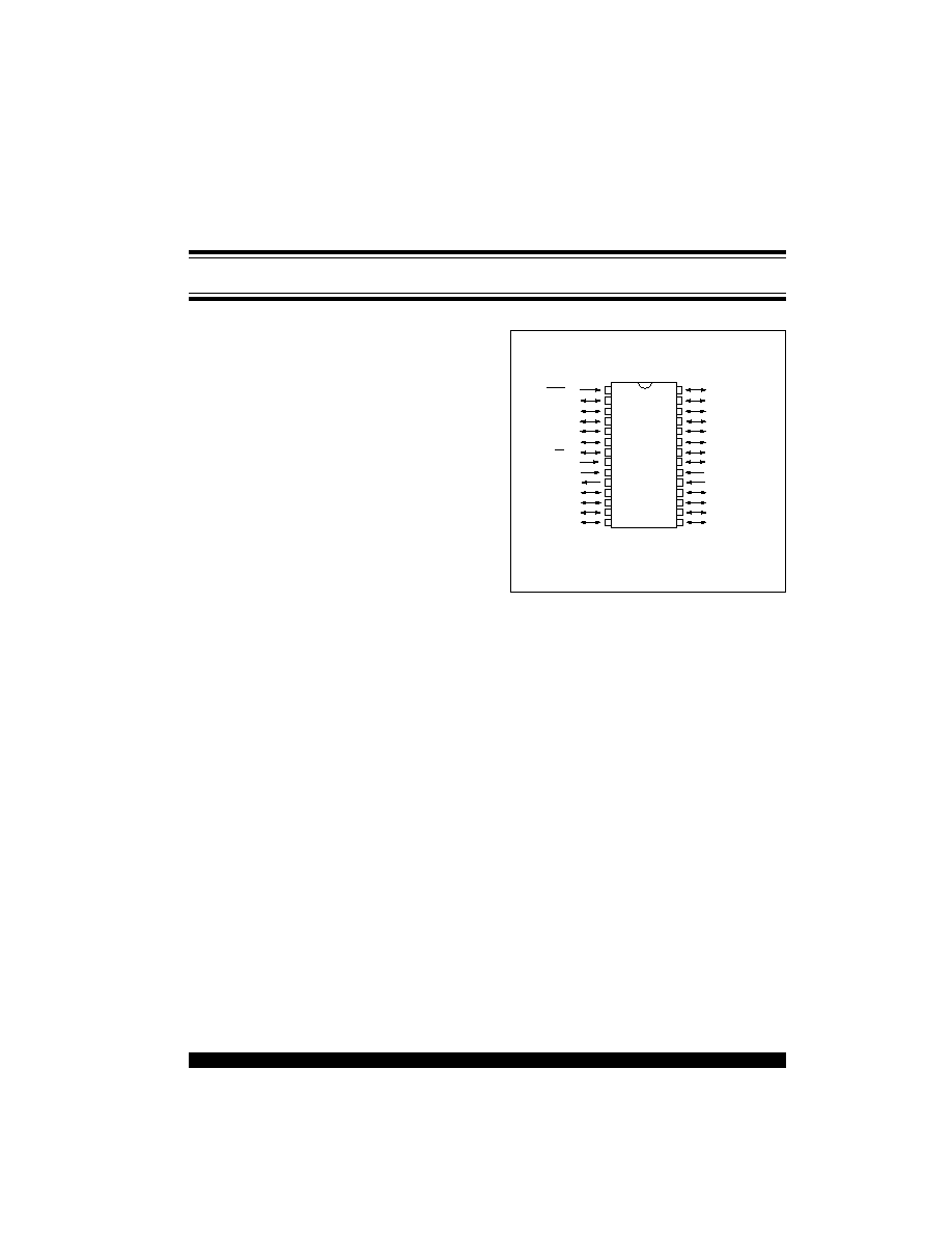
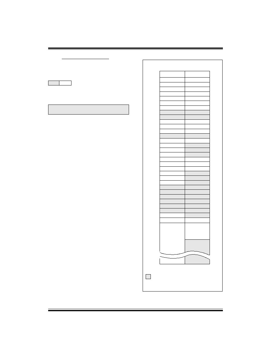
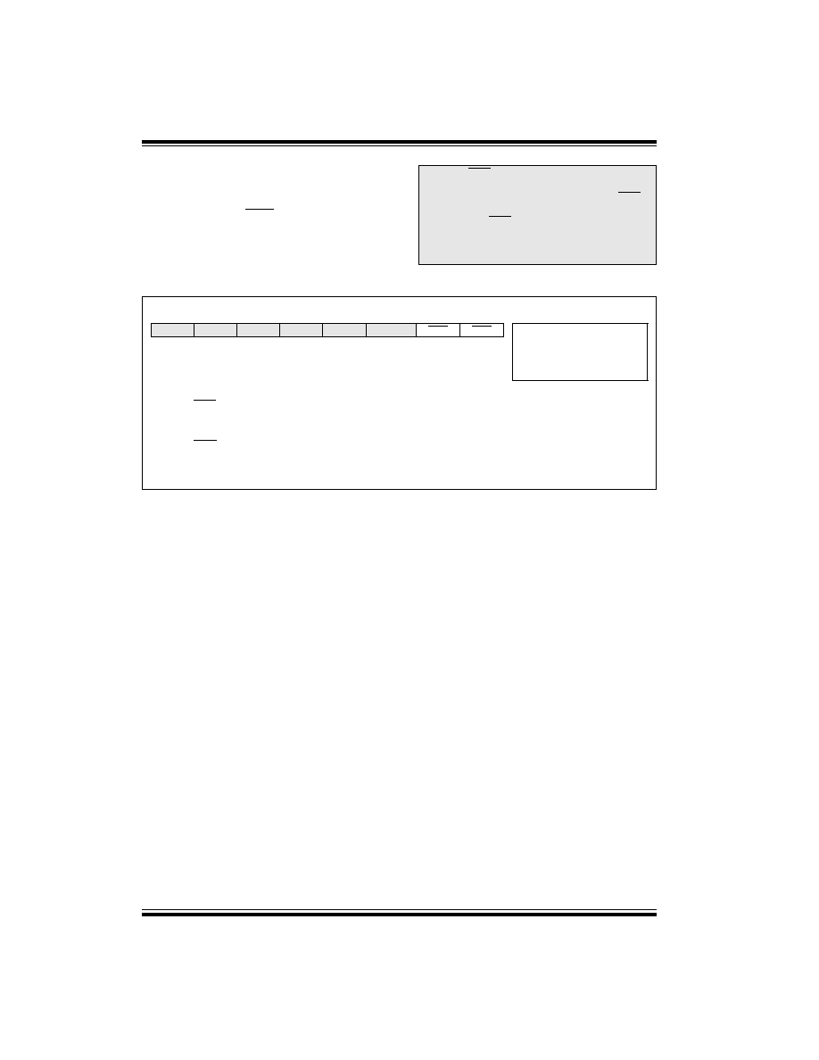
Pin Diagrams
Peripheral Features:
∑ Timer0: 8-bit timer/counter with 8-bit prescaler
∑ Timer1: 16-bit timer/counter with prescaler,
can be incremented during sleep via external
crystal/clock
∑ Timer2: 8-bit timer/counter with 8-bit period
register, prescaler and postscaler
∑ Capture, Compare, PWM (CCP) module
- Capture is 16-bit, max. resolution is 12.5 ns
- Compare is 16-bit, max. resolution is 200 ns
- PWM max. resolution is 10-bit
∑ 8-bit 5-channel analog-to-digital converter
∑ Synchronous Serial Port (SSP) with
SPI
TM
and I
2
C
TM
∑ Brown-out detection circuitry for
Brown-out Reset (BOR)
∑ PIC16C72
∑ PIC16CR72
PIC16C72
MCLR/V
PP
RA0/AN0
RA1/AN1
RA2/AN2
RA3/AN3/V
REF
RA4/T0CKI
RA5/SS/AN4
V
SS
OSC1/CLKIN
OSC2/CLKOUT
RC0/T1OSO/T1CKI
RC1/T1OSI
RC2/CCP1
RC3/SCK/SCL
RB7
RB6
RB5
RB4
RB3
RB2
RB1
RB0/INT
V
DD
V
SS
RC7
RC6
RC5/SDO
RC4/SDI/SDA
∑ 1
2
3
4
5
6
7
8
9
10
11
12
13
14
28
27
26
25
24
23
22
21
20
19
18
17
16
15
SDIP, SOIC, SSOP,
PIC16CR72
Windowed Side Brazed Ceramic
PIC16C72 SERIES
8-Bit CMOS Microcontrollers with A/D Converter

PIC16C72 Series
DS39016A-page 2
Preliminary
©
1998 Microchip Technology Inc.
Table of Contents
1.0
Device Overview .......................................................................................................................................................................... 3
2.0
Memory Organization ................................................................................................................................................................... 5
3.0
I/O Ports ..................................................................................................................................................................................... 19
4.0
Timer0 Module ........................................................................................................................................................................... 25
5.0
Timer1 Module ........................................................................................................................................................................... 27
6.0
Timer2 Module ........................................................................................................................................................................... 31
7.0
Capture/Compare/PWM (CCP) Module ..................................................................................................................................... 33
8.0
Synchronous Serial Port (SSP) Module ..................................................................................................................................... 39
9.0
Analog-to-Digital Converter (A/D) Module.................................................................................................................................. 53
10.0 Special Features of the CPU...................................................................................................................................................... 59
11.0 Instruction Set Summary ............................................................................................................................................................ 73
12.0 Development Support................................................................................................................................................................. 75
13.0 Electrical Characteristics - PIC16C72 Series ............................................................................................................................. 77
14.0 DC and AC Characteristics Graphs and Tables - PIC16C72 ..................................................................................................... 97
15.0 DC and AC Characteristics Graphs and Tables - PIC16CR72 ................................................................................................ 107
16.0 Packaging Information.............................................................................................................................................................. 109
Appendix A:
What's New in this Data Sheet .................................................................................................................................. 115
Appendix B:
What's Changed in this Data Sheet ........................................................................................................................... 115
Appendix C:
Device Differences..................................................................................................................................................... 115
Index .................................................................................................................................................................................................. 117
On-Line Support................................................................................................................................................................................. 121
Reader Response .............................................................................................................................................................................. 122
PIC16C72 Series Product Identification System................................................................................................................................ 125
Sales and Support.............................................................................................................................................................................. 125
To Our Valued Customers
We constantly strive to improve the quality of all our products and documentation. We have spent an exceptional
amount of time to ensure that these documents are correct. However, we realize that we may have missed a few
things. If you find any information that is missing or appears in error, please use the reader response form in the
back of this data sheet to inform us. We appreciate your assistance in making this a better document.
Key Reference Manual Features
PIC16C72
PIC16CR72
Operating Frequency
DC - 20MHz
DC - 20MHz
Resets
POR, PWRT, OST, BOR
POR, PWRT, OST, BOR
Program Memory - (14-bit words)
2K (EPROM)
2K (ROM)
Data Memory - RAM (8-bit bytes)
128
128
Interrupts
8
8
I/O Ports
PortA, PortB, PortC
PortA, PortB, PortC
Timers
Timer0, Timer1, Timer2
Timer0, Timer1, Timer2
Capture/Compare/PWM Modules
1
1
Serial Communications
Basic SSP
SSP
8-Bit A/D Converter
5 channels
5 channels
Instruction Set (No. of Instructions)
35
35
PIC16C72 Series
©
1998 Microchip Technology Inc.
Preliminary
DS39016A-page 3
1.0
DEVICE OVERVIEW
This document contains device-specific information for
the operation of the PIC16C72 device. Additional infor-
mation may be found in the PICmicroTM Mid-Range
MCU Reference Manual (DS33023) which may be
downloaded from the Microchip website. The Refer-
ence Manual should be considered a complementary
document to this data sheet, and is highly recom-
mended reading for a better understanding of the
device architecture and operation of the peripheral
modules.
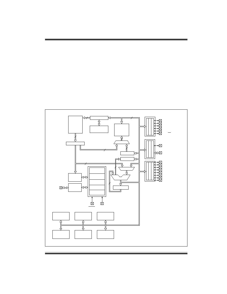
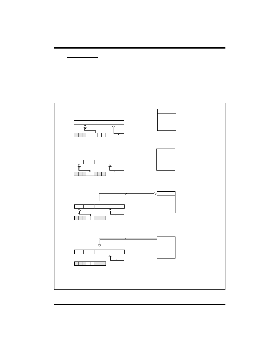
The PIC16C72 belongs to the Mid-Range family of the
PICmicro devices. A block diagram of the device is
shown in Figure 1-1.
The program memory contains 2K words which trans-
late to 2048 instructions, since each 14-bit program
memory word is the same width as each device instruc-
tion. The data memory (RAM) contains 128 bytes.
There are also 22 I/O pins that are user-configurable on
a pin-to-pin basis. Some pins are multiplexed with other
device functions. These functions include:
∑ External interrupt
∑ Change on PORTB interrupt
∑ Timer0 clock input
∑ Timer1 clock/oscillator
∑ Capture/Compare/PWM
∑ A/D converter
∑ SPI/I
2
C
Table 1-1 details the pinout of the device with descrip-
tions and details for each pin.
FIGURE 1-1:
PIC16C72/CR72 BLOCK DIAGRAM
EPROM/
Program
Memory
2K x 14
13
Data Bus
8
14
Program
Bus
Instruction reg
Program Counter
8 Level Stack
(13-bit)
RAM
File
Registers
128 x 8
Direct Addr
7
RAM Addr
(1)
9
Addr MUX
Indirect
Addr
FSR reg
STATUS reg
MUX
ALU
W reg
Power-up
Timer
Oscillator
Start-up Timer
Power-on
Reset
Watchdog
Timer
Instruction
Decode &
Control
Timing
Generation
OSC1/CLKIN
OSC2/CLKOUT
MCLR
V
DD
, V
SS
Timer0
A/D
Synchronous
Serial Port
PORTA
PORTB
PORTC
RB0/INT
RB7:RB1
RC0/T1OSO/T1CKI
RC1/T1OSI
RC2/CCP1
RC3/SCK/SCL
RC4/SDI/SDA
RC5/SDO
RC6
RC7
8
8
Brown-out
Reset
Note 1:
Higher order bits are from the STATUS register.
CCP1
Timer1
Timer2
RA4/T0CKI
RA5/SS/AN4
RA3/AN3/V
REF
RA2/AN2
RA1/AN1
RA0/AN0
8
3
ROM
PIC16C72 Series
DS39016A-page 4
Preliminary
©
1998 Microchip Technology Inc.
TABLE 1-1
PIC16C72/CR72 PINOUT DESCRIPTION
Pin Name
Pin#
I/O/P
Type
Buffer
Type
Description
OSC1/CLKIN
9
I
ST/CMOS
(3)
Oscillator crystal input/external clock source input.
OSC2/CLKOUT
10
O
--
Oscillator crystal output. Connects to crystal or resonator in crystal
oscillator mode. In RC mode, the OSC2 pin outputs CLKOUT which
has 1/4 the frequency of OSC1, and denotes the instruction cycle rate.
MCLR/V
PP
1
I/P
ST
Master clear (reset) input or programming voltage input. This pin is an
active low reset to the device.
PORTA is a bi-directional I/O port.
RA0/AN0
2
I/O
TTL
RA0 can also be analog input0.
RA1/AN1
3
I/O
TTL
RA1 can also be analog input1.
RA2/AN2
4
I/O
TTL
RA2 can also be analog input2.
RA3/AN3/V
REF
5
I/O
TTL
RA3 can also be analog input3 or analog reference voltage
RA4/T0CKI
6
I/O
ST
RA4 can also be the clock input to the Timer0 module. Output is
open drain type.
RA5/SS/AN4
7
I/O
TTL
RA5 can also be analog input4 or the slave select for the
synchronous serial port.
PORTB is a bi-directional I/O port. PORTB can be software
programmed for internal weak pull-up on all inputs.
RB0/INT
21
I/O
TTL/ST
(1)
RB0 can also be the external interrupt pin.
RB1
22
I/O
TTL
RB2
23
I/O
TTL
RB3
24
I/O
TTL
RB4
25
I/O
TTL
Interrupt on change pin.
RB5
26
I/O
TTL
Interrupt on change pin.
RB6
27
I/O
TTL/ST
(2)
Interrupt on change pin. Serial programming clock.
RB7
28
I/O
TTL/ST
(2)
Interrupt on change pin. Serial programming data.
PORTC is a bi-directional I/O port.
RC0/T1OSO/T1CKI
11
I/O
ST
RC0 can also be the Timer1 oscillator output or Timer1 clock
input.
RC1/T1OSI
12
I/O
ST
RC1 can also be the Timer1 oscillator input.
RC2/CCP1
13
I/O
ST
RC2 can also be the Capture1 input/Compare1 output/PWM1
output.
RC3/SCK/SCL
14
I/O
ST
RC3 can also be the synchronous serial clock input/output for both
SPI and I
2
C modes.
RC4/SDI/SDA
15
I/O
ST
RC4 can also be the SPI Data In (SPI mode) or
data I/O (I
2
C mode).
RC5/SDO
16
I/O
ST
RC5 can also be the SPI Data Out (SPI mode).
RC6
17
I/O
ST
RC7
18
I/O
ST
V
SS
8, 19
P
--
Ground reference for logic and I/O pins.
V
DD
20
P
--
Positive supply for logic and I/O pins.
Legend: I = input
O = output
I/O = input/output
P = power
-- = Not used
TTL = TTL input
ST = Schmitt Trigger input
Note 1:
This buffer is a Schmitt Trigger input when configured as the external interrupt.
2:
This buffer is a Schmitt Trigger input when used in serial programming mode.
3:
This buffer is a Schmitt Trigger input when configured in RC oscillator mode and a CMOS input otherwise
.
PIC16C72 Series
©
1998 Microchip Technology Inc.
Preliminary
DS39016A-page 5
2.0
MEMORY ORGANIZATION
There are two memory blocks in PIC16C72 Series
devices. These are the program memory and the data
memory. Each block has its own bus, so that access to
both blocks can occur during the same oscillator cycle.
The data memory can further be broken down into the
general purpose RAM and the Special Function
Registers (SFRs). The operation of the SFRs that
control the "core" are described here. The SFRs used
to control the peripheral modules are described in the
section discussing each individual peripheral module.
Additional information on device memory may be found
in the PICmicroTM Mid-Range Reference Manual,
DS33023.
2.1
Program Memory Organization
PIC16C72 Series devices have a 13-bit program
counter capable of addressing a 2K x 14 program
memory space. The address range for this program
memory is 0000h - 07FFh. Accessing a location above
the physically implemented address will cause a wrap-
around.
The reset vector is at 0000h and the interrupt vector is
at 0004h.
FIGURE 2-1:
PROGRAM MEMORY MAP
AND STACK
PC<12:0>
13
0000h
0004h
0005h
07FFh
1FFFh
Stack Level 1
Stack Level 8
Reset Vector
Interrupt Vector
On-chip Program
Memory
CALL, RETURN
RETFIE, RETLW
0800h
User Memor
y
Space
PIC16C72 Series
DS39016A-page 6
Preliminary
©
1998 Microchip Technology Inc.
2.2
Data Memory Organization
The data memory is partitioned into multiple banks
which contain the General Purpose Registers and the
Special Function Registers. Bits RP1 and RP0 are the
bank select bits.
= 00
Bank0
= 01
Bank1
= 10
Bank2 (not implemented)
= 11
Bank3 (not implemented)
Each bank extends up to 7Fh (128 bytes). The lower
locations of each bank are reserved for the Special
Function Registers. Above the Special Function Regis-
ters are General Purpose Registers, implemented as
static RAM.
All implemented banks contain special function regis-
ters. Some "high use" special function registers from
one bank may be mirrored in another bank for code
reduction and quicker access (ex; the STATUS register
is in Bank 0 and Bank 1).
2.2.1
GENERAL PURPOSE REGISTER FILE
The register file can be accessed either directly or indi-
rectly through the File Select Register FSR
(Section
2.5).
FIGURE 2-2:
REGISTER FILE MAP
RP1*
RP0
(STATUS<6:5>)
*
Maintain this bit clear to ensure upward com-
patibility with future products.
INDF
(1)
TMR0
PCL
STATUS
FSR
PORTA
PORTB
PORTC
PCLATH
INTCON
PIR1
TMR1L
TMR1H
T1CON
TMR2
T2CON
SSPBUF
SSPCON
CCPR1L
CCPR1H
CCP1CON
ADRES
ADCON0
INDF
(1)
OPTION
PCL
STATUS
FSR
TRISA
TRISB
TRISC
PCLATH
INTCON
PIE1
PCON
PR2
SSPADD
SSPSTAT
ADCON1
00h
01h
02h
03h
04h
05h
06h
07h
08h
09h
0Ah
0Bh
0Ch
0Dh
0Eh
0Fh
10h
11h
12h
13h
14h
15h
16h
17h
18h
19h
1Ah
1Bh
1Ch
1Dh
1Eh
1Fh
80h
81h
82h
83h
84h
85h
86h
87h
88h
89h
8Ah
8Bh
8Ch
8Dh
8Eh
8Fh
90h
91h
92h
93h
94h
95h
96h
97h
98h
99h
9Ah
9Bh
9Ch
9Dh
9Eh
9Fh
20h
A0h
General
Purpose
Register
General
Purpose
Register
7Fh
FFh
Bank 0
Bank 1
File
Address
BFh
C0h
Unimplemented data memory locations, read as '0'.
Note 1:
Not a physical register.
File
Address
PIC16C72 Series
©
1998 Microchip Technology Inc.
Preliminary
DS39016A-page 7
2.2.2
SPECIAL FUNCTION REGISTERS
The Special Function Registers are registers used by
the CPU and Peripheral Modules for controlling the
desired operation of the device. These registers are
implemented as static RAM.
The special function registers can be classified into two
sets (core and peripheral). Those registers associated
with the "core" functions are described in this section,
and those related to the operation of the peripheral fea-
tures are described in the section of that peripheral fea-
ture.
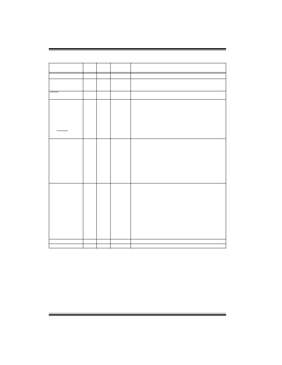
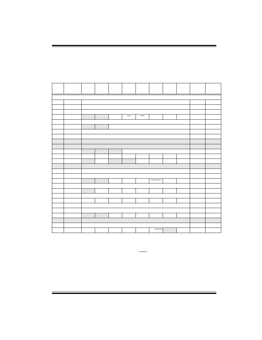
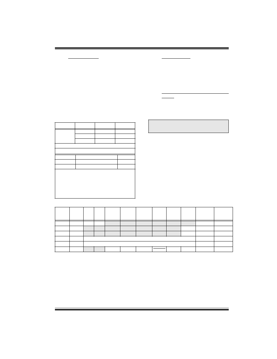
TABLE 2-1
SPECIAL FUNCTION REGISTER SUMMARY
Address Name
Bit 7
Bit 6
Bit 5
Bit 4
Bit 3
Bit 2
Bit 1
Bit 0
Value on:
POR,
BOR
Value on all
other resets
(3)
Bank 0
00h
(1)
INDF
Addressing this location uses contents of FSR to address data memory (not a physical register)
0000 0000
0000 0000
01h
TMR0
Timer0 module's register
xxxx xxxx
uuuu uuuu
02h
(1)
PCL
Program Counter's (PC) Least Significant Byte
0000 0000
0000 0000
03h
(1)
STATUS
IRP
(4)
RP1
(4)
RP0
TO
PD
Z
DC
C
0001 1xxx
000q quuu
04h
(1)
FSR
Indirect data memory address pointer
xxxx xxxx
uuuu uuuu
05h
PORTA
--
--
PORTA Data Latch when written: PORTA pins when read
--0x 0000
--0u 0000
06h
PORTB
PORTB Data Latch when written: PORTB pins when read
xxxx xxxx
uuuu uuuu
07h
PORTC
PORTC Data Latch when written: PORTC pins when read
xxxx xxxx
uuuu uuuu
08h
--
Unimplemented
--
--
09h
--
Unimplemented
--
--
0Ah
(1,2)
PCLATH
--
--
--
Write Buffer for the upper 5 bits of the Program Counter
---0 0000
---0 0000
0Bh
(1)
INTCON
GIE
PEIE
T0IE
INTE
RBIE
T0IF
INTF
RBIF
0000 000x
0000 000u
0Ch
PIR1
--
ADIF
--
--
SSPIF
CCP1IF
TMR2IF
TMR1IF
-0-- 0000
-0-- 0000
0Dh
--
Unimplemented
--
--
0Eh
TMR1L
Holding register for the Least Significant Byte of the 16-bit TMR1 register
xxxx xxxx
uuuu uuuu
0Fh
TMR1H
Holding register for the Most Significant Byte of the 16-bit TMR1 register
xxxx xxxx
uuuu uuuu
10h
T1CON
--
--
T1CKPS1
T1CKPS0
T1OSCEN
T1SYNC
TMR1CS
TMR1ON
--00 0000
--uu uuuu
11h
TMR2
Timer2 module's register
0000 0000
0000 0000
12h
T2CON
--
TOUTPS3
TOUTPS2
TOUTPS1
TOUTPS0
TMR2ON
T2CKPS1
T2CKPS0
-000 0000
-000 0000
13h
SSPBUF
Synchronous Serial Port Receive Buffer/Transmit Register
xxxx xxxx
uuuu uuuu
14h
SSPCON
WCOL
SSPOV
SSPEN
CKP
SSPM3
SSPM2
SSPM1
SSPM0
0000 0000
0000 0000
15h
CCPR1L
Capture/Compare/PWM Register (LSB)
xxxx xxxx
uuuu uuuu
16h
CCPR1H
Capture/Compare/PWM Register (MSB)
xxxx xxxx
uuuu uuuu
17h
CCP1CON
--
--
CCP1X
CCP1Y
CCP1M3
CCP1M2
CCP1M1
CCP1M0
--00 0000
--00 0000
18h-1Dh
--
Unimplemented
--
--
1Eh
ADRES
A/D Result Register
xxxx xxxx
uuuu uuuu
1Fh
ADCON0
ADCS1
ADCS0
CHS2
CHS1
CHS0
GO/DONE
--
ADON
0000 00-0
0000 00-0
Legend:
x
= unknown,
u
= unchanged,
q
= value depends on condition, - = unimplemented read as '0'.
Shaded locations are unimplemented, read as `0'.
Note 1:
These registers can be addressed from either bank.
2:
The upper byte of the program counter is not directly accessible. PCLATH is a holding register for the PC<12:8> whose con-
tents are transferred to the upper byte of the program counter.
3:
Other (non power-up) resets include external reset through MCLR and Watchdog Timer Reset.
4:
The IRP and RP1 bits are reserved on the PIC16C72/CR72. Always maintain these bits clear.
5:
SSPSTAT<7:6> are not implemented on the PIC16C72, read as '0'.
PIC16C72 Series
DS39016A-page 8
Preliminary
©
1998 Microchip Technology Inc.
Bank 1
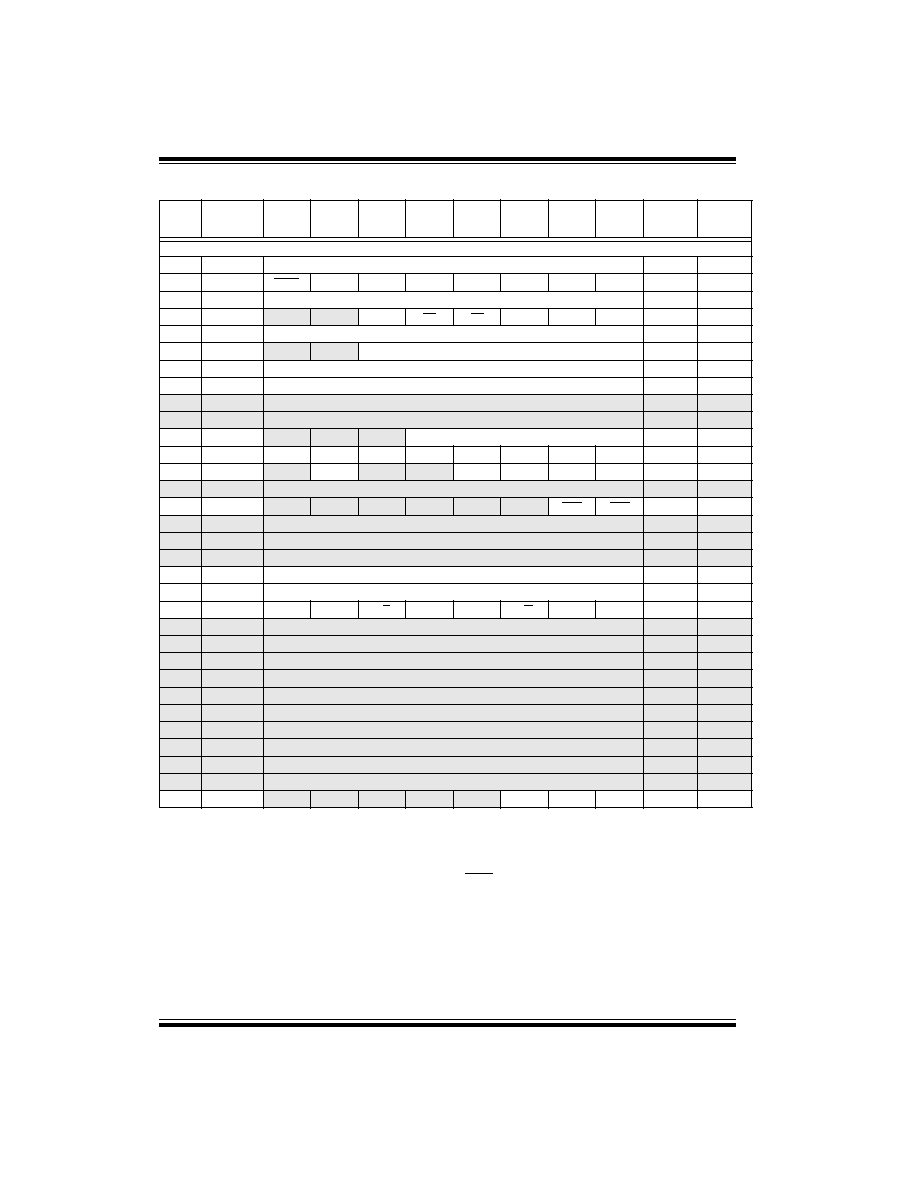
80h
(1)
INDF
Addressing this location uses contents of FSR to address data memory (not a physical register)
0000 0000
0000 0000
81h
OPTION_REG
RBPU
INTEDG
T0CS
T0SE
PSA
PS2
PS1
PS0
1111 1111
1111 1111
82h
(1)
PCL
Program Counter's (PC) Least Significant Byte
0000 0000
0000 0000
83h
(1)
STATUS
IRP
(4)
RP1
(4)
RP0
TO
PD
Z
DC
C
0001 1xxx
000q quuu
84h
(1)
FSR
Indirect data memory address pointer
xxxx xxxx
uuuu uuuu
85h
TRISA
--
--
PORTA Data Direction Register
--11 1111
--11 1111
86h
TRISB
PORTB Data Direction Register
1111 1111
1111 1111
87h
TRISC
PORTC Data Direction Register
1111 1111
1111 1111
88h
--
Unimplemented
--
--
89h
--
Unimplemented
--
--
8Ah
(1,2)
PCLATH
--
--
--
Write Buffer for the upper 5 bits of the PC
---0 0000
---0 0000
8Bh
(1)
INTCON
GIE
PEIE
T0IE
INTE
RBIE
T0IF
INTF
RBIF
0000 000x
0000 000u
8Ch
PIE1
--
ADIE
--
--
SSPIE
CCP1IE
TMR2IE
TMR1IE
-0-- 0000
-0-- 0000
8Dh
--
Unimplemented
--
--
8Eh
PCON
--
--
--
--
--
--
POR
BOR
---- --qq
---- --uu
8Fh
--
Unimplemented
--
--
90h
--
Unimplemented
--
--
91h
--
Unimplemented
--
--
92h
PR2
Timer2 Period Register
1111 1111
1111 1111
93h
SSPADD
Synchronous Serial Port (I
2
C mode) Address Register
0000 0000
0000 0000
94h
SSPSTAT
SMP
(5)
CKE
(5)
D/A
P
S
R/W
UA
BF
0000 0000
0000 0000
95h
--
Unimplemented
--
--
96h
--
Unimplemented
--
--
97h
--
Unimplemented
--
--
98h
--
Unimplemented
--
--
99h
--
Unimplemented
--
--
9Ah
--
Unimplemented
--
--
9Bh
--
Unimplemented
--
--
9Ch
--
Unimplemented
--
--
9Dh
--
Unimplemented
--
--
9Eh
--
Unimplemented
--
--
9Fh
ADCON1
--
--
--
--
--
PCFG2
PCFG1
PCFG0
---- -000 ---- -000
TABLE 2-1
SPECIAL FUNCTION REGISTER SUMMARY (CONTINUED)
Address Name
Bit 7
Bit 6
Bit 5
Bit 4
Bit 3
Bit 2
Bit 1
Bit 0
Value on:
POR,
BOR
Value on all
other resets
(3)
Legend:
x
= unknown,
u
= unchanged,
q
= value depends on condition, - = unimplemented read as '0'.
Shaded locations are unimplemented, read as `0'.
Note 1:
These registers can be addressed from either bank.
2:
The upper byte of the program counter is not directly accessible. PCLATH is a holding register for the PC<12:8> whose con-
tents are transferred to the upper byte of the program counter.
3:
Other (non power-up) resets include external reset through MCLR and Watchdog Timer Reset.
4:
The IRP and RP1 bits are reserved on the PIC16C72/CR72. Always maintain these bits clear.
5:
SSPSTAT<7:6> are not implemented on the PIC16C72, read as '0'.
PIC16C72 Series
©
1998 Microchip Technology Inc.
Preliminary
DS39016A-page 9
2.2.2.1
STATUS REGISTER
The STATUS register, shown in Figure 2-3, contains
the arithmetic status of the ALU, the RESET status and
the bank select bits for data memory.
The STATUS register can be the destination for any
instruction, as with any other register. If the STATUS
register is the destination for an instruction that affects
the Z, DC or C bits, then the write to these three bits is
disabled. These bits are set or cleared according to the
device logic. Furthermore, the TO and PD bits are not
writable. Therefore, the result of an instruction with the
STATUS register as destination may be different than
intended.
For example,
CLRF STATUS
will clear the upper-three
bits and set the Z bit. This leaves the STATUS register
as
000u u1uu
(where
u
= unchanged).
It is recommended, therefore, that only
BCF, BSF,
SWAPF
and
MOVWF
instructions are used to alter the
STATUS register because these instructions do not
affect the Z, C or DC bits from the STATUS register. For
other instructions, not affecting any status bits, see the
"Instruction Set Summary."
FIGURE 2-3:
STATUS REGISTER (ADDRESS 03h, 83h)
Note 1: These devices do not use bits IRP and
RP1 (STATUS<7:6>). Maintain these bits
clear to ensure upward compatibility with
future products.
Note 2: The C and DC bits operate as a borrow
and digit borrow bit, respectively, in sub-
traction. See the
SUBLW
and
SUBWF
instructions for examples.
R/W-0
R/W-0
R/W-0
R-1
R-1
R/W-x
R/W-x
R/W-x
IRP
RP1
RP0
TO
PD
Z
DC
C
R = Readable bit
W = Writable bit
U = Unimplemented bit,
read as `0'
- n = Value at POR reset
bit7
bit0
bit 7:
IRP: Register Bank Select bit (used for indirect addressing)
1 = Bank 2, 3 (100h - 1FFh)
0 = Bank 0, 1 (00h - FFh)
bit 6-5: RP1:RP0: Register Bank Select bits (used for direct addressing)
11
= Bank 3 (180h - 1FFh)
10
= Bank 2 (100h - 17Fh)
01
= Bank 1 (80h - FFh)
00
= Bank 0 (00h - 7Fh)
Each bank is 128 bytes. For devices with only Bank0 and Bank1, the IRP bit is reserved. Always maintain
this bit clear.
bit 4:
TO: Time-out bit
1 = After power-up,
CLRWDT
instruction, or
SLEEP
instruction
0 = A WDT time-out occurred
bit 3:
PD: Power-down bit
1 = After power-up or by the
CLRWDT
instruction
0 = By execution of the
SLEEP
instruction
bit 2:
Z: Zero bit
1 = The result of an arithmetic or logic operation is zero
0 = The result of an arithmetic or logic operation is not zero
bit 1:
DC: Digit carry/borrow bit (
ADDWF
,
ADDLW,SUBLW,SUBWF
instructions) (for borrow the polarity is reversed)
1 = A carry-out from the 4th low order bit of the result occurred
0 = No carry-out from the 4th low order bit of the result
bit 0:
C: Carry/borrow bit (
ADDWF
,
ADDLW,SUBLW,SUBWF
instructions)
1 = A carry-out from the most significant bit of the result occurred
0 = No carry-out from the most significant bit of the result occurred
Note: For borrow the polarity is reversed. A subtraction is executed by adding the two's complement of the
second operand. For rotate (
RRF
,
RLF
) instructions, this bit is loaded with either the high or low order bit of
the source register.

PIC16C72 Series
DS39016A-page 10
Preliminary
©
1998 Microchip Technology Inc.
2.2.2.2
OPTION_REG REGISTER
The OPTION_REG register is a readable and writable
register which contains various control bits to configure
the TMR0 prescaler/WDT postscaler (single assign-
able register known also as the prescaler), the External
INT Interrupt, TMR0, and the weak pull-ups on PORTB.
FIGURE 2-4:
OPTION_REG REGISTER
(ADDRESS 81h)
Note:
To achieve a 1:1 prescaler assignment for
the TMR0 register, assign the prescaler to
the Watchdog Timer.
R/W-1
R/W-1
R/W-1
R/W-1
R/W-1
R/W-1
R/W-1
R/W-1
RBPU
INTEDG
T0CS
T0SE
PSA
PS2
PS1
PS0
R
= Readable bit
W = Writable bit
U
= Unimplemented bit,
read as `0'
- n = Value at POR reset
bit7
bit0
bit 7:
RBPU: PORTB Pull-up Enable bit
1 = PORTB pull-ups are disabled
0 = PORTB pull-ups are enabled by individual port latch values
bit 6:
INTEDG: Interrupt Edge Select bit
1 = Interrupt on rising edge of RB0/INT pin
0 = Interrupt on falling edge of RB0/INT pin
bit 5:
T0CS: TMR0 Clock Source Select bit
1 = Transition on RA4/T0CKI pin
0 = Internal instruction cycle clock (CLKOUT)
bit 4:
T0SE: TMR0 Source Edge Select bit
1 = Increment on high-to-low transition on RA4/T0CKI pin
0 = Increment on low-to-high transition on RA4/T0CKI pin
bit 3:
PSA: Prescaler Assignment bit
1 = Prescaler is assigned to the WDT
0 = Prescaler is assigned to the Timer0 module
bit 2-0: PS2:PS0: Prescaler Rate Select bits
000
001
010
011
100
101
110
111
1 : 2
1 : 4
1 : 8
1 : 16
1 : 32
1 : 64
1 : 128
1 : 256
1 : 1
1 : 2
1 : 4
1 : 8
1 : 16
1 : 32
1 : 64
1 : 128
Bit Value
TMR0 Rate
WDT Rate

PIC16C72 Series
©
1998 Microchip Technology Inc.
Preliminary
DS39016A-page 11
2.2.2.3
INTCON REGISTER
The INTCON Register is a readable and writable regis-
ter which contains various enable and flag bits for the
TMR0 register overflow, RB Port change and External
RB0/INT pin interrupts.
FIGURE 2-5:
INTCON REGISTER (ADDRESS 0Bh, 8Bh)
Note:
Interrupt flag bits get set when an interrupt
condition occurs regardless of the state of
its corresponding enable bit or the global
enable bit, GIE (INTCON<7>). User soft-
ware should ensure the appropriate inter-
rupt flag bits are clear prior to enabling an
interrupt.
R/W-0
R/W-0
R/W-0
R/W-0
R/W-0
R/W-0
R/W-0
R/W-x
GIE
PEIE
T0IE
INTE
RBIE
T0IF
INTF
RBIF
R
= Readable bit
W = Writable bit
U
= Unimplemented bit,
read as `0'
- n = Value at POR reset
bit7
bit0
bit 7:
GIE: Global Interrupt Enable bit
1 = Enables all un-masked interrupts
0 = Disables all interrupts
bit 6:
PEIE: Peripheral Interrupt Enable bit
1 = Enables all un-masked peripheral interrupts
0 = Disables all peripheral interrupts
bit 5:
T0IE: TMR0 Overflow Interrupt Enable bit
1 = Enables the TMR0 interrupt
0 = Disables the TMR0 interrupt
bit 4:
INTE: RB0/INT External Interrupt Enable bit
1 = Enables the RB0/INT external interrupt
0 = Disables the RB0/INT external interrupt
bit 3:
RBIE: RB Port Change Interrupt Enable bit
1 = Enables the RB port change interrupt
0 = Disables the RB port change interrupt
bit 2:
T0IF: TMR0 Overflow Interrupt Flag bit
1 = TMR0 register has overflowed (must be cleared in software)
0 = TMR0 register did not overflow
bit 1:
INTF: RB0/INT External Interrupt Flag bit
1 = The RB0/INT external interrupt occurred (must be cleared in software)
0 = The RB0/INT external interrupt did not occur
bit 0:
RBIF: RB Port Change Interrupt Flag bit
1 = At least one of the RB7:RB4 pins changed state (must be cleared in software)
0 = None of the RB7:RB4 pins have changed state

PIC16C72 Series
DS39016A-page 12
Preliminary
©
1998 Microchip Technology Inc.
2.2.2.4
PIE1 REGISTER
This register contains the individual enable bits for the
peripheral interrupts.
FIGURE 2-6:
PIE1 REGISTER (ADDRESS 8Ch)
Note:
Bit PEIE (INTCON<6>) must be set to
enable any peripheral interrupt.
U-0
R/W-0
U-0
U-0
R/W-0
R/W-0
R/W-0
R/W-0
--
ADIE
--
--
SSPIE
CCP1IE
TMR2IE
TMR1IE
R
= Readable bit
W = Writable bit
U
= Unimplemented bit,
read as `0'
- n = Value at POR reset
bit7
bit0
bit 7:
Unimplemented: Read as '0'
bit 6:
ADIE: A/D Converter Interrupt Enable bit
1 = Enables the A/D interrupt
0 = Disables the A/D interrupt
bit 5-4: Unimplemented: Read as '0'
bit 3:
SSPIE: Synchronous Serial Port Interrupt Enable bit
1 = Enables the SSP interrupt
0 = Disables the SSP interrupt
bit 2:
CCP1IE: CCP1 Interrupt Enable bit
1 = Enables the CCP1 interrupt
0 = Disables the CCP1 interrupt
bit 1:
TMR2IE: TMR2 to PR2 Match Interrupt Enable bit
1 = Enables the TMR2 to PR2 match interrupt
0 = Disables the TMR2 to PR2 match interrupt
bit 0:
TMR1IE: TMR1 Overflow Interrupt Enable bit
1 = Enables the TMR1 overflow interrupt
0 = Disables the TMR1 overflow interrupt

PIC16C72 Series
©
1998 Microchip Technology Inc.
Preliminary
DS39016A-page 13
2.2.2.5
PIR1 REGISTER
This register contains the individual flag bits for the
Peripheral interrupts.
FIGURE 2-7:
PIR1 REGISTER (ADDRESS 0Ch)
Note:
Interrupt flag bits get set when an interrupt
condition occurs regardless of the state of
its corresponding enable bit or the global
enable bit, GIE (INTCON<7>). User soft-
ware should ensure the appropriate inter-
rupt flag bits are clear prior to enabling an
interrupt.
U-0
R/W-0
U-0
U-0
R/W-0
R/W-0
R/W-0
R/W-0
--
ADIF
--
--
SSPIF
CCP1IF
TMR2IF
TMR1IF
R
= Readable bit
W = Writable bit
U
= Unimplemented bit,
read as `0'
- n = Value at POR reset
bit7
bit0
bit 7:
Unimplemented: Read as '0'
bit 6:
ADIF: A/D Converter Interrupt Flag bit
1 = An A/D conversion completed (must be cleared in software)
0 = The A/D conversion is not complete
bit 5-4: Unimplemented: Read as '0'
bit 3:
SSPIF: Synchronous Serial Port Interrupt Flag bit
1 = The transmission/reception is complete (must be cleared in software)
0 = Waiting to transmit/receive
bit 2:
CCP1IF: CCP1 Interrupt Flag bit
Capture Mode
1 = A TMR1 register capture occurred (must be cleared in software)
0 = No TMR1 register capture occurred
Compare Mode
1 = A TMR1 register compare match occurred (must be cleared in software)
0 = No TMR1 register compare match occurred
PWM Mode
Unused in this mode
bit 1:
TMR2IF: TMR2 to PR2 Match Interrupt Flag bit
1 = TMR2 to PR2 match occurred (must be cleared in software)
0 = No TMR2 to PR2 match occurred
bit 0:
TMR1IF: TMR1 Overflow Interrupt Flag bit
1 = TMR1 register overflowed (must be cleared in software)
0 = TMR1 register did not overflow
PIC16C72 Series
DS39016A-page 14
Preliminary
©
1998 Microchip Technology Inc.
2.2.2.6
PCON REGISTER
The Power Control (PCON) register contains a flag bit
to allow differentiation between a Power-on Reset
(POR) to an external MCLR Reset or WDT Reset.
Those devices with brown-out detection circuitry con-
tain an additional bit to differentiate a Brown-out Reset
condition from a Power-on Reset condition.
FIGURE 2-8:
PCON REGISTER (ADDRESS 8Eh)
Note:
BOR is unknown on Power-on Reset. It
must then be set by the user and checked
on subsequent resets to see if BOR is
clear, indicating a brown-out has occurred.
The BOR status bit is a don't care and is
not necessarily predictable if the brown-out
circuit is disabled (by clearing the BODEN
bit in the Configuration word).
U-0
U-0
U-0
U-0
U-0
U-0
R/W-0
R/W-q
--
--
--
--
--
--
POR
BOR
R
= Readable bit
W = Writable bit
U
= Unimplemented bit,
read as `0'
- n = Value at POR reset
bit7
bit0
bit 7-2:
Unimplemented: Read as '0'
bit 1:
POR: Power-on Reset Status bit
1 = No Power-on Reset occurred
0 = A Power-on Reset occurred (must be set in software after a Power-on Reset occurs)
bit 0:
BOR: Brown-out Reset Status bit
1 = No Brown-out Reset occurred
0 = A Brown-out Reset occurred (must be set in software after a Brown-out Reset occurs)
PIC16C72 Series
©
1998 Microchip Technology Inc.
Preliminary
DS39016A-page 15
2.3
PCL and PCLATH
The program counter (PC) specifies the address of the
instruction to fetch for execution. The PC is 13 bits
wide. The low byte is called the PCL register. This reg-
ister is readable and writable. The high byte is called
the PCH register. This register contains the PC<12:8>
bits and is not directly readable or writable. All updates
to the PCH register go through the PCLATH register.
Figure 2-9 shows the four situations for the loading of
the PC. Example 1 shows how the PC is loaded on a
write to PCL (PCLATH<4:0>
PCH). Example 2
shows how the PC is loaded during a
GOTO
instruction
(PCLATH<4:3>
PCH). Example 3 shows how the PC
is loaded during a
CALL
instruction (PCLATH<4:3>
PCH), with the PC loaded (PUSHed) onto the Top of
Stack. Finally, example 4 shows how the PC is loaded
during one of the return instructions where the PC is
loaded (POPed) from the Top of Stack.
FIGURE 2-9:
LOADING OF PC IN DIFFERENT SITUATIONS
PC
12
8
7
0
5
PCLATH<4:0>
PCLATH
ALU result
Opcode <10:0>
8
PC
12
11 10
0
11
PCLATH<4:3>
PCH
PCL
8
7
2
PCLATH
PCH
PCL
Situation 1 - Instruction with PCL as destination
Situation 2 -
GOTO
Instruction
STACK (13-bits x 8)
Top of STACK
STACK (13-bits x 8)
Top of STACK
Opcode <10:0>
PC
12
11 10
0
11
PCLATH<4:3>
8
7
2
PCLATH
PCH
PCL
Situation 3 -
CALL
Instruction
STACK (13-bits x 8)
Top of STACK
Opcode <10:0>
PC
12
11 10
0
11
8
7
PCLATH
PCH
PCL
Situation 4 -
RETURN
,
RETFIE
, or
RETLW
Instruction
STACK (13-bits x 8)
Top of STACK
13
13
Note: PCLATH is not updated with the contents of PCH.
PIC16C72 Series
DS39016A-page 16
Preliminary
©
1998 Microchip Technology Inc.
2.3.1
STACK
The stack allows a combination of up to 8 program calls
and interrupts to occur. The stack contains the return
address from this branch in program execution.
Midrange devices have an 8 level deep x 13-bit wide
hardware stack. The stack space is not part of either
program or data space and the stack pointer is not
readable or writable. The PC is PUSHed onto the stack
when a
CALL
instruction is executed or an interrupt
causes a branch. The stack is POPed in the event of a
RETURN, RETLW
or a
RETFIE
instruction execution.
PCLATH is not modified when the stack is PUSHed or
POPed.
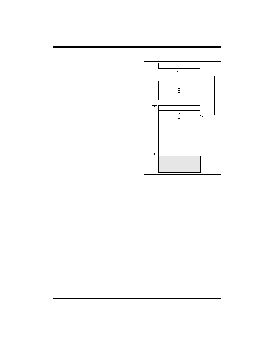
After the stack has been PUSHed eight times, the ninth
push overwrites the value that was stored from the first
push. The tenth push overwrites the second push (and
so on). An example of the overwriting of the stack is
shown in Figure 2-10.
FIGURE 2-10: STACK MODIFICATION
2.4
Program Memory Paging
The
CALL
and
GOTO
instructions provide 11 bits of
address to allow branching within any 2K program
memory page. When doing a
CALL
or
GOTO
instruction
the upper 2 bits of the address are provided by
PCLATH<4:3>. When doing a
CALL
or
GOTO
instruction,
the user must ensure that the page select bits are pro-
grammed so that the desired program memory page is
addressed. If a return from a
CALL
instruction (or inter-
rupt) is executed, the entire 13-bit PC is pushed onto
the stack. Therefore, manipulation of the
PCLATH<4:3> bits are not required for the return
instructions (which POPs the address from the stack).
Push1 Push9
Push2 Push10
Push3
Push4
Push5
Push6
Push7
Push8
Top of STACK
STACK
Note:
PIC16C72 Series devices ignore paging
bit PCLATH<4>. The use of PCLATH<4>
as a general purpose read/write bit is not
recommended since this may affect
upward compatibility with future products.
PIC16C72 Series
©
1998 Microchip Technology Inc.
Preliminary
DS39016A-page 17
2.5
Indirect Addressing, INDF and FSR
Registers
The INDF register is not a physical register. Address-
ing INDF actually addresses the register whose
address is contained in the FSR register (FSR is a
pointer). This is indirect addressing.
EXAMPLE 2-1:
INDIRECT ADDRESSING
∑ Register file 05 contains the value 10h
∑ Register file 06 contains the value 0Ah
∑ Load the value 05 into the FSR register
∑ A read of the INDF register will return the value of
10h
∑ Increment the value of the FSR register by one
(FSR = 06)
∑ A read of the INDR register now will return the
value of 0Ah.
Reading INDF itself indirectly (FSR = 0) will produce
00h. Writing to the INDF register indirectly results in a
no-operation (although STATUS bits may be affected).
A simple program to clear RAM locations 20h-2Fh
using indirect addressing is shown in Example 2-2.
EXAMPLE 2-2:
HOW TO CLEAR RAM
USING INDIRECT
ADDRESSING
movlw 0x20 ;initialize pointer
movwf FSR ; to RAM
NEXT clrf INDF ;clear INDF register
incf FSR ;inc pointer
btfss FSR,4 ;all done?
goto NEXT ;NO, clear next
CONTINUE
: ;YES, continue
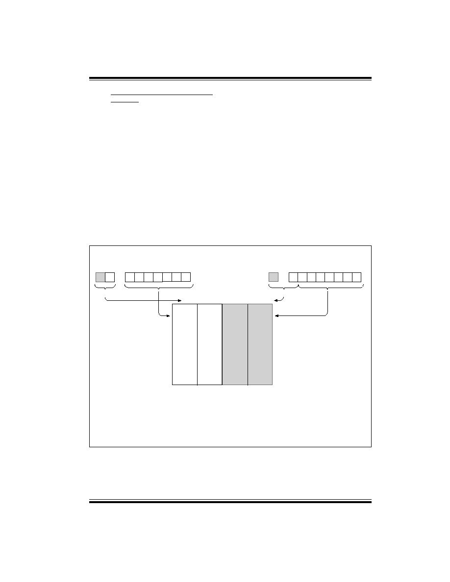
An effective 9-bit address is obtained by concatenating
the 8-bit FSR register and the IRP bit (STATUS<7>), as
shown in Figure 2-11. However, IRP is not used in the
PIC16C72 Series.
FIGURE 2-11: DIRECT/INDIRECT ADDRESSING
Note 1: For register file map detail see Figure 2-2.
2: Maintain RP1 and IRP as clear for upward compatibility with future products.
3: Not implemented.
Data
Memory(1)
Indirect Addressing
Direct Addressing
bank select
location select
RP1:RP0
6
0
from opcode
IRP
FSR register
7
0
bank select
location select
00
01
10
11
Bank 0
Bank 1
Bank 2
Bank 3
not used
FFh
80h
7Fh
00h
17Fh
100h
1FFh
180h
(2)
(2)
(3)
(3)

PIC16C72 Series
DS39016A-page 18
Preliminary
©
1998 Microchip Technology Inc.
NOTES:
PIC16C72 Series
©
1998 Microchip Technology Inc.
Preliminary
DS39016A-page 19
3.0
I/O PORTS
Some pins for these I/O ports are multiplexed with an
alternate function for the peripheral features on the
device. In general, when a peripheral is enabled, that
pin may not be used as a general purpose I/O pin.
Additional information on I/O ports may be found in the
PICmicroTM Mid-Range MCU Reference Manual,
DS33023.
3.1
PORTA and the TRISA Register
PORTA is a 6-bit wide bi-directional port. The corre-
sponding data direction register is TRISA. Setting a
TRISA bit (=1) will make the corresponding PORTA pin
an input, i.e., put the corresponding output driver in a
hi-impedance mode. Clearing a TRISA bit (=0) will
make the corresponding PORTA pin an output, i.e., put
the contents of the output latch on the selected pin.
Reading the PORTA register reads the status of the
pins whereas writing to it will write to the port latch. All
write operations are read-modify-write operations.
Therefore a write to a port implies that the port pins are
read, this value is modified, and then written to the port
data latch.
Pin RA4 is multiplexed with the Timer0 module clock
input to become the RA4/T0CKI pin. The RA4/T0CKI
pin is a Schmitt Trigger input and an open drain output.
All other RA port pins have TTL input levels and full
CMOS output drivers.
Other PORTA pins are multiplexed with analog inputs
and analog V
REF
input. The operation of each pin is
selected by clearing/setting the control bits in the
ADCON1 register (A/D Control Register1).
The TRISA register controls the direction of the RA
pins, even when they are being used as analog inputs.
The user must ensure the bits in the TRISA register are
maintained set when using them as analog inputs.
EXAMPLE 3-1:
INITIALIZING PORTA
BCF STATUS, RP0 ;
CLRF PORTA ; Initialize PORTA by
; clearing output
; data latches
BSF STATUS, RP0 ; Select Bank 1
MOVLW 0xCF ; Value used to
; initialize data
; direction
MOVWF TRISA ; Set RA<3:0> as inputs
; RA<5:4> as outputs
; TRISA<7:6> are always
; read as '0'.
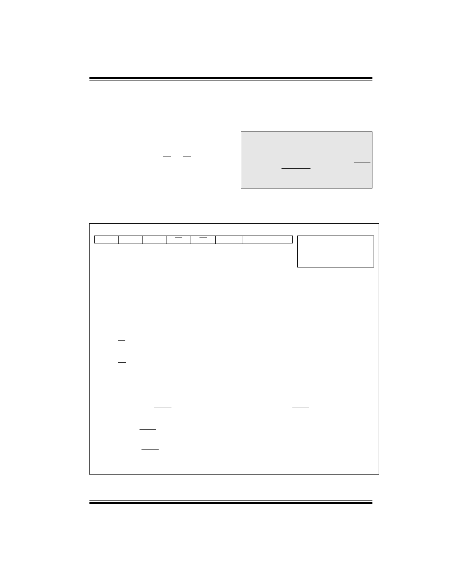
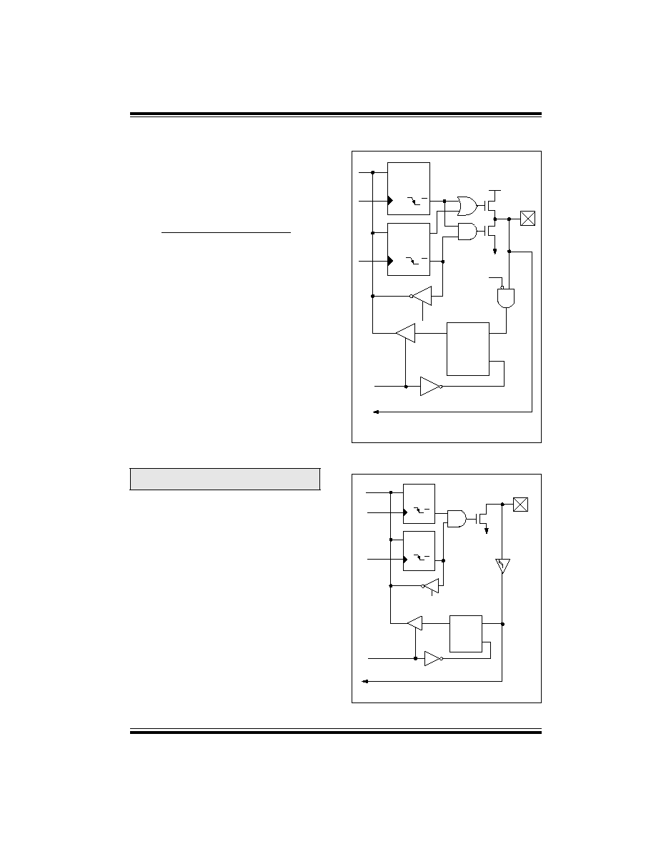
FIGURE 3-1:
BLOCK DIAGRAM OF
RA3:RA0 AND RA5 PINS
FIGURE 3-2:
BLOCK DIAGRAM OF RA4/
T0CKI PIN
Note:
On a Power-on Reset, these pins are con-
figured as analog inputs and read as '0'.
Data
bus
Q
D
Q
CK
Q
D
Q
CK
Q
D
EN
P
N
WR
Port
WR
TRIS
Data Latch
TRIS Latch
RD TRIS
RD PORT
V
SS
V
DD
I/O pin
(1)
Note 1:
I/O pins have protection diodes to V
DD
and
V
SS
.
Analog
input
mode
TTL
input
buffer
To A/D Converter
Data
bus
WR
PORT
WR
TRIS
RD PORT
Data Latch
TRIS Latch
RD TRIS
Schmitt
Trigger
input
buffer
N
V
SS
I/O pin
(1)
TMR0 clock input
Note 1: I/O pin has protection diodes to V
SS
only.
Q
D
Q
CK
Q
D
Q
CK
EN
Q
D
EN
PIC16C72 Series
DS39016A-page 20
Preliminary
©
1998 Microchip Technology Inc.
TABLE 3-1
PORTA FUNCTIONS
TABLE 3-2
SUMMARY OF REGISTERS ASSOCIATED WITH PORTA
Name
Bit#
Buffer
Function
RA0/AN0
bit0
TTL
Input/output or analog input
RA1/AN1
bit1
TTL
Input/output or analog input
RA2/AN2
bit2
TTL
Input/output or analog input
RA3/AN3/V
REF
bit3
TTL
Input/output or analog input or V
REF
RA4/T0CKI
bit4
ST
Input/output or external clock input for Timer0
Output is open drain type
RA5/SS/AN4
bit5
TTL
Input/output or slave select input for synchronous serial port or analog input
Legend: TTL = TTL input, ST = Schmitt Trigger input
Address Name
Bit 7
Bit 6
Bit 5
Bit 4
Bit 3
Bit 2
Bit 1
Bit 0
Value on:
POR,
BOR
Value on all
other resets
05h
PORTA
--
--
RA5
RA4
RA3
RA2
RA1
RA0
--0x 0000
--0u 0000
85h
TRISA
--
--
PORTA Data Direction Register
--11 1111
--11 1111
9Fh
ADCON1
--
--
--
--
--
PCFG2
PCFG1
PCFG0
---- -000
---- -000
Legend:
x
= unknown,
u
= unchanged,
-
= unimplemented locations read as '0'. Shaded cells are not used by PORTA.
PIC16C72 Series
©
1998 Microchip Technology Inc.
Preliminary
DS39016A-page 21
3.2
PORTB and the TRISB Register
PORTB is an 8-bit wide bi-directional port. The corre-
sponding data direction register is TRISB. Setting a
TRISB bit (=1) will make the corresponding PORTB pin
an input, i.e., put the corresponding output driver in a
hi-impedance mode. Clearing a TRISB bit (=0) will
make the corresponding PORTB pin an output, i.e., put
the contents of the output latch on the selected pin.
EXAMPLE 3-1:
INITIALIZING PORTB
BCF STATUS, RP0 ;
CLRF PORTB ; Initialize PORTB by
; clearing output
; data latches
BSF STATUS, RP0 ; Select Bank 1
MOVLW 0xCF ; Value used to
; initialize data
; direction
MOVWF TRISB ; Set RB<3:0> as inputs
; RB<5:4> as outputs
; RB<7:6> as inputs
Each of the PORTB pins has a weak internal pull-up. A
single control bit can turn on all the pull-ups. This is per-
formed by clearing bit RBPU (OPTION<7>). The weak
pull-up is automatically turned off when the port pin is
configured as an output. The pull-ups are disabled on a
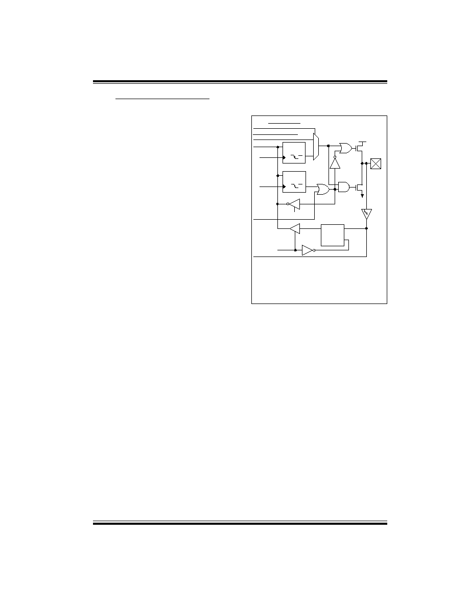
Power-on Reset.
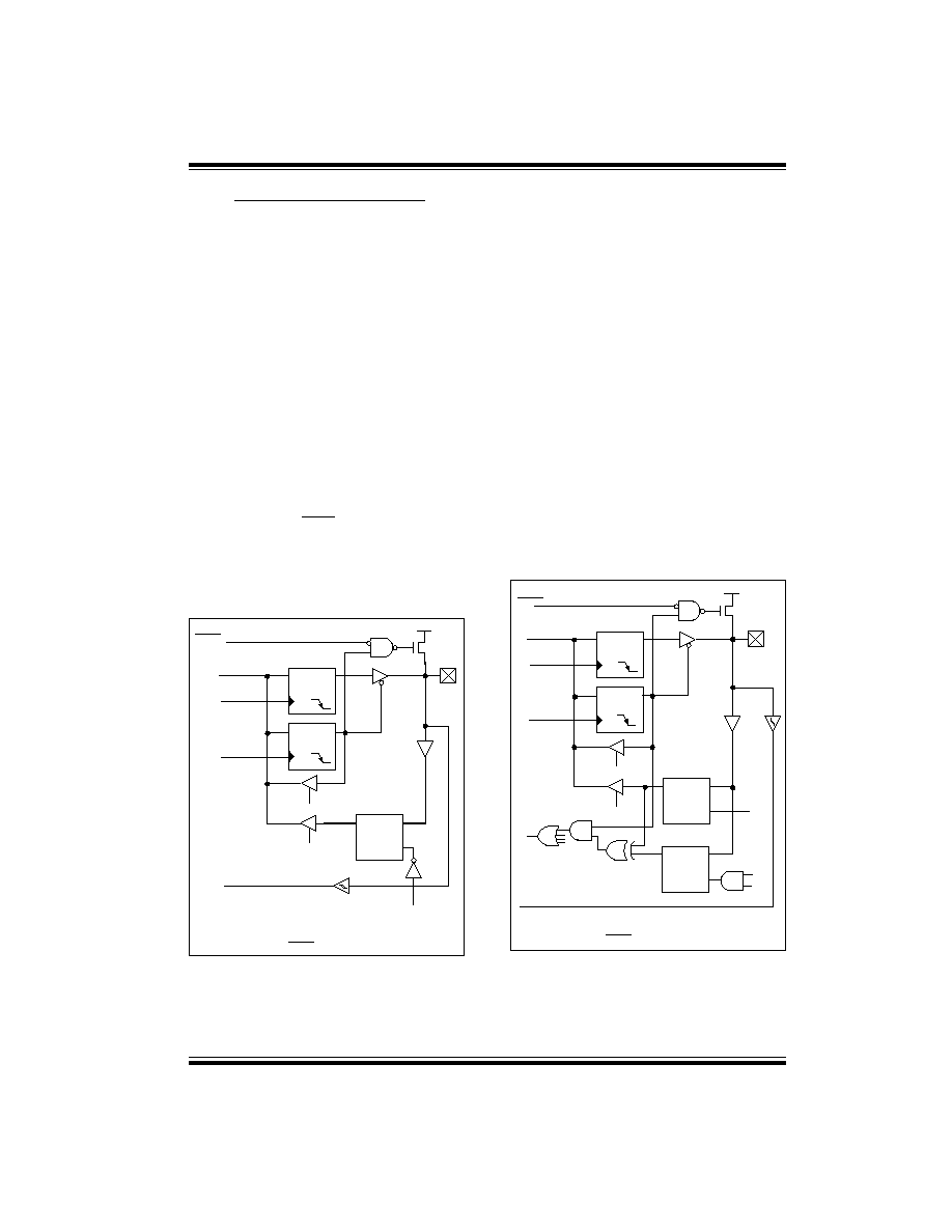
FIGURE 3-3:
BLOCK DIAGRAM OF
RB3:RB0 PINS
Four of PORTB's pins, RB7:RB4, have an interrupt on
change feature. Only pins configured as inputs can
cause this interrupt to occur (i.e. any RB7:RB4 pin con-
figured as an output is excluded from the interrupt on
change comparison). The input pins (of RB7:RB4) are
compared with the old value latched on the last read of
PORTB. The "mismatch" outputs of RB7:RB4 are
OR'ed together to generate the RB Port Change Inter-
rupt with flag bit RBIF (INTCON<0>).
This interrupt can wake the device from SLEEP. The
user, in the interrupt service routine, can clear the inter-
rupt in the following manner:
a)
Any read or write of PORTB. This will end the
mismatch condition.
b)
Clear flag bit RBIF.
A mismatch condition will continue to set flag bit RBIF.
Reading PORTB will end the mismatch condition, and
allow flag bit RBIF to be cleared.
The interrupt on change feature is recommended for
wake-up on key depression operation and operations
where PORTB is only used for the interrupt on change
feature. Polling of PORTB is not recommended while
using the interrupt on change feature.
FIGURE 3-4:
BLOCK DIAGRAM OF
RB7:RB4 PINS
Data Latch
RBPU
(2)
P
V
DD
Q
D
CK
Q
D
CK
Q
D
EN
Data bus
WR Port
WR TRIS
RD TRIS
RD Port
weak
pull-up
RD Port
RB0/INT
I/O
pin
(1)
TTL
Input
Buffer
Note 1: I/O pins have diode protection to V
DD
and V
SS
.
2: To enable weak pull-ups, set the appropriate TRIS bit(s)
and clear the RBPU bit (OPTION<7>).
Schmitt Trigger
Buffer
TRIS Latch
Data Latch
From other
RBPU
(2)
P
V
DD
I/O
Q
D
CK
Q
D
CK
Q
D
EN
Q
D
EN
Data bus
WR Port
WR TRIS
Set RBIF
TRIS Latch
RD TRIS
RD Port
RB7:RB4 pins
weak
pull-up
RD Port
Latch
TTL
Input
Buffer
pin
(1)
Note 1: I/O pins have diode protection to V
DD
and V
SS
.
ST
Buffer
RB7:RB6 in serial programming mode
Q3
Q1
2: To enable weak pull-ups, set the appropriate TRIS bit(s)
and clear the RBPU bit (OPTION<7>).
PIC16C72 Series
DS39016A-page 22
Preliminary
©
1998 Microchip Technology Inc.
TABLE 3-3
PORTB FUNCTIONS
TABLE 3-4
SUMMARY OF REGISTERS ASSOCIATED WITH PORTB
Name
Bit#
Buffer
Function
RB0/INT
bit0
TTL/ST
(1)
Input/output pin or external interrupt input. Internal software
programmable weak pull-up.
RB1
bit1
TTL
Input/output pin. Internal software programmable weak pull-up.
RB2
bit2
TTL
Input/output pin. Internal software programmable weak pull-up.
RB3
bit3
TTL
Input/output pin. Internal software programmable weak pull-up.
RB4
bit4
TTL
Input/output pin (with interrupt on change). Internal software programmable
weak pull-up.
RB5
bit5
TTL
Input/output pin (with interrupt on change). Internal software programmable
weak pull-up.
RB6
bit6
TTL/ST
(2)
Input/output pin (with interrupt on change). Internal software programmable
weak pull-up. Serial programming clock.
RB7
bit7
TTL/ST
(2)
Input/output pin (with interrupt on change). Internal software programmable
weak pull-up. Serial programming data.
Legend: TTL = TTL input, ST = Schmitt Trigger input
Note 1: This buffer is a Schmitt Trigger input when configured as the external interrupt.
2: This buffer is a Schmitt Trigger input when used in serial programming mode.
Address
Name
Bit 7
Bit 6
Bit 5
Bit 4
Bit 3
Bit 2
Bit 1
Bit 0
Value on:
POR,
BOR
Value on all
other resets
06h, 106h
PORTB
RB7
RB6
RB5
RB4
RB3
RB2
RB1
RB0
xxxx xxxx
uuuu uuuu
86h, 186h
TRISB
PORTB Data Direction Register
1111 1111
1111 1111
81h, 181h
OPTION
RBPU
INTEDG
T0CS
T0SE
PSA
PS2
PS1
PS0
1111 1111
1111 1111
Legend:
x
= unknown,
u
= unchanged. Shaded cells are not used by PORTB.
PIC16C72 Series
©
1998 Microchip Technology Inc.
Preliminary
DS39016A-page 23
3.3
PORTC and the TRISC Register
PORTC is an 8-bit wide bi-directional port. The corre-
sponding data direction register is TRISC. Setting a
TRISC bit (=1) will make the corresponding PORTC pin
an input, i.e., put the corresponding output driver in a
hi-impedance mode. Clearing a TRISC bit (=0) will
make the corresponding PORTC pin an output, i.e., put
the contents of the output latch on the selected pin.
PORTC is multiplexed with several peripheral functions
(Table 3-5). PORTC pins have Schmitt Trigger input
buffers.
When enabling peripheral functions, care should be
taken in defining TRIS bits for each PORTC pin. Some
peripherals override the TRIS bit to make a pin an out-
put, while other peripherals override the TRIS bit to
make a pin an input. Since the TRIS bit override is in
effect while the peripheral is enabled, read-modify-
write instructions (
BSF, BCF, XORWF
) with TRISC as
destination should be avoided. The user should refer to
the corresponding peripheral section for the correct
TRIS bit settings.
EXAMPLE 3-1:
INITIALIZING PORTC
BCF STATUS, RP0 ; Select Bank 0
CLRF PORTC ; Initialize PORTC by
; clearing output
; data latches
BSF STATUS, RP0 ; Select Bank 1
MOVLW 0xCF ; Value used to
; initialize data
; direction
MOVWF TRISC ; Set RC<3:0> as inputs
; RC<5:4> as outputs
; RC<7:6> as inputs
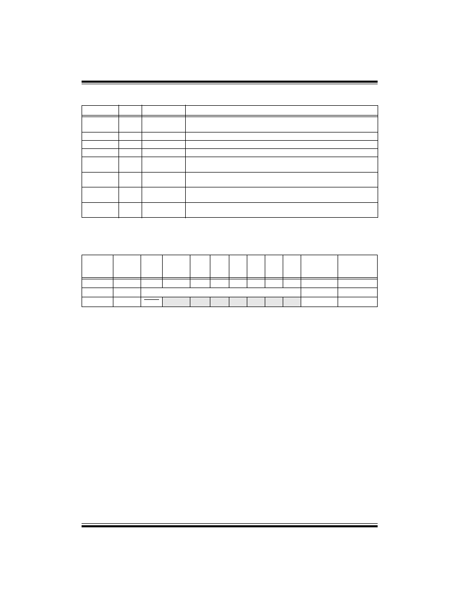
FIGURE 3-5:
PORTC BLOCK DIAGRAM
(PERIPHERAL OUTPUT
OVERRIDE)
PORT/PERIPHERAL Select
(2)
Data bus
WR
PORT
WR
TRIS
RD
Data Latch
TRIS Latch
RD TRIS
Schmitt
Trigger
Q
D
Q
CK
Q
D
EN
Peripheral Data Out
0
1
Q
D
Q
CK
P
N
V
DD
V
SS
PORT
Peripheral
OE
(3)
Peripheral input
I/O
pin
(1)
Note 1:
I/O pins have diode protection to V
DD
and V
SS
.
2:
Port/Peripheral select signal selects between port
data and peripheral output.
3:
Peripheral OE (output enable) is only activated if
peripheral select is active.
PIC16C72 Series
DS39016A-page 24
Preliminary
©
1998 Microchip Technology Inc.
TABLE 3-5
PORTC FUNCTIONS
TABLE 3-6
SUMMARY OF REGISTERS ASSOCIATED WITH PORTC
Name
Bit#
Buffer Type
Function
RC0/T1OSO/T1CKI
bit0
ST
Input/output port pin or Timer1 oscillator output/Timer1 clock input
RC1/T1OSI
bit1
ST
Input/output port pin or Timer1 oscillator input
RC2/CCP1
bit2
ST
Input/output port pin or Capture1 input/Compare1 output/PWM1
output
RC3/SCK/SCL
bit3
ST
RC3 can also be the synchronous serial clock for both SPI and I
2
C
modes.
RC4/SDI/SDA
bit4
ST
RC4 can also be the SPI Data In (SPI mode) or data I/O (I
2
C mode).
RC5/SDO
bit5
ST
Input/output port pin or Synchronous Serial Port data output
RC6
bit6
ST
Input/output port pin
RC7
bit7
ST
Input/output port pin
Legend: ST = Schmitt Trigger input
Address Name
Bit 7
Bit 6
Bit 5
Bit 4
Bit 3
Bit 2
Bit 1
Bit 0
Value on:
POR,
BOR
Value on all
other resets
07h
PORTC
RC7
RC6
RC5
RC4
RC3
RC2
RC1
RC0
xxxx xxxx
uuuu uuuu
87h
TRISC
PORTC Data Direction Register
1111 1111
1111 1111
Legend:
x
= unknown,
u
= unchanged.
PIC16C72 Series
©
1998 Microchip Technology Inc.
Preliminary
DS39016A-page 25
4.0
TIMER0 MODULE
The Timer0 module timer/counter has the following fea-
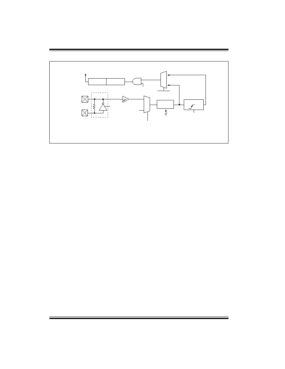
tures:
∑ 8-bit timer/counter
∑ Readable and writable
∑ Internal or external clock select
∑ Edge select for external clock
∑ 8-bit software programmable prescaler
∑ Interrupt on overflow from FFh to 00h
Figure 4-1 is a simplified block diagram of the Timer0
module.
Additional information on timer modules is available in
the PICmicroTM Mid-Range MCU Reference Manual,
DS33023.
4.1
Timer0 Operation
Timer0 can operate as a timer or as a counter.
Timer mode is selected by clearing bit T0CS
(OPTION_REG<5>). In timer mode, the Timer0 mod-
ule will increment every instruction cycle (without pres-
caler). If the TMR0 register is written, the increment is
inhibited for the following two instruction cycles. The
user can work around this by writing an adjusted value
to the TMR0 register.
Counter mode is selected by setting bit T0CS
(OPTION_REG<5>). In counter mode, Timer0 will
increment either on every rising or falling edge of pin
RA4/T0CKI. The incrementing edge is determined by
the Timer0 Source Edge Select bit T0SE
(OPTION_REG<4>). Clearing bit T0SE selects the ris-
ing edge. Restrictions on the external clock input are
discussed in below.
When an external clock input is used for Timer0, it must
meet certain requirements. The requirements ensure
the external clock can be synchronized with the internal
phase clock (T
OSC
). Also, there is a delay in the actual
incrementing of Timer0 after synchronization.
Additional information on external clock requirements
is available in the PICmicroTM Mid-Range MCU Refer-
ence Manual, DS33023.
4.2
Prescaler
An 8-bit counter is available as a prescaler for the
Timer0 module, or as a postscaler for the Watchdog
Timer, respectively (Figure 4-2). For simplicity, this
counter is being referred to as "prescaler" throughout
this data sheet. Note that there is only one prescaler
available which is mutually exclusively shared between
the Timer0 module and the Watchdog Timer. Thus, a
prescaler assignment for the Timer0 module means
that there is no prescaler for the Watchdog Timer, and
vice-versa.
The prescaler is not readable or writable.
The PSA and PS2:PS0 bits (OPTION_REG<3:0>)
determine the prescaler assignment and prescale ratio.
Clearing bit PSA will assign the prescaler to the Timer0
module. When the prescaler is assigned to the Timer0
module, prescale values of 1:2, 1:4, ..., 1:256 are
selectable.
Setting bit PSA will assign the prescaler to the Watch-
dog Timer (WDT). When the prescaler is assigned to
the WDT, prescale values of 1:1, 1:2, ..., 1:128 are
selectable.
When assigned to the Timer0 module, all instructions
writing to the TMR0 register (e.g.
CLRF 1, MOVWF 1,
BSF 1,x
....etc.) will clear the prescaler. When assigned
to WDT, a
CLRWDT
instruction will clear the prescaler
along with the WDT.
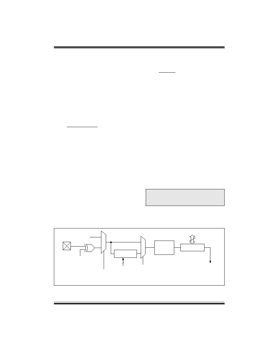
FIGURE 4-1:
TIMER0 BLOCK DIAGRAM
Note:
Writing to TMR0 when the prescaler is
assigned to Timer0 will clear the prescaler
count, but will not change the prescaler
assignment.
Note 1: T0CS, T0SE, PSA, PS2:PS0 (OPTION_REG<5:0>).
2: The prescaler is shared with Watchdog Timer (refer to Figure 4-2 for detailed block diagram).
RA4/T0CKI
T0SE
0
1
1
0
pin
T0CS
F
OSC
/4
Programmable
Prescaler
Sync with
Internal
clocks
TMR0
PSout
(2 cycle delay)
PSout
Data bus
8
PSA
PS2, PS1, PS0
Set interrupt
flag bit T0IF
on overflow
3
PIC16C72 Series
DS39016A-page 26
Preliminary
©
1998 Microchip Technology Inc.
4.2.1
SWITCHING PRESCALER ASSIGNMENT
The prescaler assignment is fully under software con-
trol, i.e., it can be changed "on the fly" during program
execution.
4.3
Timer0 Interrupt
The TMR0 interrupt is generated when the TMR0 reg-
ister overflows from FFh to 00h. This overflow sets bit
T0IF (INTCON<2>). The interrupt can be masked by
clearing bit T0IE (INTCON<5>). Bit T0IF must be
cleared in software by the Timer0 module interrupt ser-
vice routine before re-enabling this interrupt. The TMR0
interrupt cannot awaken the processor from SLEEP
since the timer is shut off during SLEEP.
FIGURE 4-2:
BLOCK DIAGRAM OF THE TIMER0/WDT PRESCALER
TABLE 4-1
REGISTERS ASSOCIATED WITH TIMER0
Note:
To avoid an unintended device RESET, a
specific instruction sequence (shown in the
PICmicroTM Mid-Range MCU Reference
Manual, DS3023) must be executed when
changing the prescaler assignment from
Timer0 to the WDT. This sequence must be
followed even if the WDT is disabled.
Address
Name
Bit 7
Bit 6
Bit 5
Bit 4
Bit 3
Bit 2
Bit 1
Bit 0
Value on:
POR,
BOR
Value on all
other resets
01h,101h
TMR0
Timer0 module's register
xxxx xxxx
uuuu uuuu
0Bh,8Bh,
10Bh,18Bh
INTCON
GIE
PEIE
T0IE
INTE
RBIE
T0IF
INTF
RBIF
0000 000x
0000 000u
81h,181h
OPTION_REG
RBPU
INTEDG
T0CS
T0SE
PSA
PS2
PS1
PS0
1111 1111
1111 1111
85h
TRISA
--
--
PORTA Data Direction Register
--11 1111
--11 1111
Legend:
x
= unknown,
u
= unchanged,
-
= unimplemented locations read as '0'. Shaded cells are not used by Timer0.
RA4/T0CKI
T0SE
pin
M
U
X
CLKOUT (=Fosc/4)
SYNC
2
Cycles
TMR0 reg
8-bit Prescaler
8 - to - 1MUX
M
U
X
M U X
Watchdog
Timer
PSA
0
1
0
1
WDT
Time-out
PS2:PS0
8
Note: T0CS, T0SE, PSA, PS2:PS0 are (OPTION_REG<5:0>).
PSA
WDT Enable bit
M
U
X
0
1
0
1
Data Bus
Set flag bit T0IF
on Overflow
8
PSA
T0CS

PIC16C72 Series
©
1998 Microchip Technology Inc.
Preliminary
DS39016A-page 27
5.0
TIMER1 MODULE
The Timer1 module timer/counter has the following fea-
tures:
∑ 16-bit timer/counter
(Two 8-bit registers; TMR1H and TMR1L)
∑ Readable and writable (Both registers)
∑ Internal or external clock select
∑ Interrupt on overflow from FFFFh to 0000h
∑ Reset from CCP module trigger
Timer1 has a control register, shown in Figure 5-1.
Timer1 can be enabled/disabled by setting/clearing
control bit TMR1ON (T1CON<0>).
Figure 5-2 is a simplified block diagram of the Timer1
module.
Additional information on timer modules is available in
the PICmicroTM Mid-Range MCU Reference Manual,
DS33023.
5.1
Timer1 Operation
Timer1 can operate in one of these modes:
∑ As a timer
∑ As a synchronous counter
∑ As an asynchronous counter
The operating mode is determined by the clock select
bit, TMR1CS (T1CON<1>).
In timer mode, Timer1 increments every instruction
cycle. In counter mode, it increments on every rising
edge of the external clock input.
When the Timer1 oscillator is enabled (T1OSCEN is
set), the RC1/T1OSI and RC0/T1OSO/T1CKI pins
become inputs. That is, the TRISC<1:0> value is
ignored.
Timer1 also has an internal "reset input". This reset can
be generated by the CCP module (Section 7.0).
FIGURE 5-1:
T1CON: TIMER1 CONTROL REGISTER
(ADDRESS 10h)
U-0
U-0
R/W-0
R/W-0
R/W-0
R/W-0
R/W-0
R/W-0
--
--
T1CKPS1 T1CKPS0 T1OSCEN
T1SYNC
TMR1CS TMR1ON
R
= Readable bit
W = Writable bit
U
= Unimplemented bit,
read as `0'
- n = Value at POR reset
bit7
bit0
bit 7-6:
Unimplemented: Read as '0'
bit 5-4: T1CKPS1:T1CKPS0: Timer1 Input Clock Prescale Select bits
11
= 1:8 Prescale value
10
= 1:4 Prescale value
01
= 1:2 Prescale value
00
= 1:1 Prescale value
bit 3:
T1OSCEN: Timer1 Oscillator Enable Control bit
1 = Oscillator is enabled
0 = Oscillator is shut off
Note: The oscillator inverter and feedback resistor are turned off to eliminate power drain
bit 2:
T1SYNC: Timer1 External Clock Input Synchronization Control bit
TMR1CS = 1
1 = Do not synchronize external clock input
0 = Synchronize external clock input
TMR1CS = 0
This bit is ignored. Timer1 uses the internal clock when TMR1CS = 0.
bit 1:
TMR1CS: Timer1 Clock Source Select bit
1 = External clock from pin RC0/T1OSO/T1CKI (on the rising edge)
0 = Internal clock (F
OSC
/4)
bit 0:
TMR1ON: Timer1 On bit
1 = Enables Timer1
0 = Stops Timer1
PIC16C72 Series
DS39016A-page 28
Preliminary
©
1998 Microchip Technology Inc.
FIGURE 5-2:
TIMER1 BLOCK DIAGRAM
TMR1H
TMR1L
T1OSC
T1SYNC
TMR1CS
T1CKPS1:T1CKPS0
SLEEP input
T1OSCEN
Enable
Oscillator
(1)
F
OSC
/4
Internal
Clock
TMR1ON
on/off
Prescaler
1, 2, 4, 8
Synchronize
det
1
0
0
1
Synchronized
clock input
2
RC0/T1OSO/T1CKI
RC1/T1OSI
Note 1:
When the T1OSCEN bit is cleared, the inverter and feedback resistor are turned off. This eliminates power drain.
Set flag bit
TMR1IF on
Overflow
TMR1
PIC16C72 Series
©
1998 Microchip Technology Inc.
Preliminary
DS39016A-page 29
5.2
Timer1 Oscillator
A crystal oscillator circuit is built in between pins T1OSI
(input) and T1OSO (amplifier output). It is enabled by
setting control bit T1OSCEN (T1CON<3>). The oscilla-
tor is a low power oscillator rated up to 200 kHz. It will
continue to run during SLEEP. It is primarily intended
for a 32 kHz crystal. Table 5-1 shows the capacitor
selection for the Timer1 oscillator.
The Timer1 oscillator is identical to the LP oscillator.
The user must provide a software time delay to ensure
proper oscillator start-up.
TABLE 5-1
CAPACITOR SELECTION
FOR THE TIMER1
OSCILLATOR
5.3
Timer1 Interrupt
The TMR1 Register pair (TMR1H:TMR1L) increments
from 0000h to FFFFh and rolls over to 0000h. The
TMR1 Interrupt, if enabled, is generated on overflow
which is latched in interrupt flag bit TMR1IF (PIR1<0>).
This interrupt can be enabled/disabled by setting/clear-
ing TMR1 interrupt enable bit TMR1IE (PIE1<0>).
5.4
Resetting Timer1 using a CCP Trigger
Output
If the CCP module is configured in compare mode to
generate a "special event trigger" (CCP1M3:CCP1M0
=
1011
), this signal will reset Timer1 and start an A/D
conversion (if the A/D module is enabled).
Timer1 must be configured for either timer or synchro-
nized counter mode to take advantage of this feature. If
Timer1 is running in asynchronous counter mode, this
reset operation may not work.
In the event that a write to Timer1 coincides with a spe-
cial event trigger from CCP1, the write will take prece-
dence.
In this mode of operation, the CCPR1H:CCPR1L regis-
ters pair effectively becomes the period register for
Timer1.
TABLE 5-2
REGISTERS ASSOCIATED WITH TIMER1 AS A TIMER/COUNTER
Osc Type
Freq
C1
C2
LP
32 kHz
33 pF
33 pF
100 kHz
15 pF
15 pF
200 kHz
15 pF
15 pF
These values are for design guidance only.
Crystals Tested:
32.768 kHz
Epson C-001R32.768K-A
±
20 PPM
100 kHz
Epson C-2 100.00 KC-P
±
20 PPM
200 kHz
STD XTL 200.000 kHz
±
20 PPM
Note 1: Higher capacitance increases the stability
of oscillator but also increases the start-up
time.
2: Since each resonator/crystal has its own
characteristics, the user should consult the
resonator/crystal manufacturer for appropri-
ate values of external components.
Note:
The special event triggers from the CCP1
module will not set interrupt flag bit
TMR1IF (PIR1<0>).
Address
Name
Bit 7
Bit 6
Bit 5
Bit 4
Bit 3
Bit 2
Bit 1
Bit 0
Value on:
POR,
BOR
Value on
all other
resets
0Bh,8Bh
INTCON
GIE
PEIE
T0IE
INTE
RBIE
T0IF
INTF
RBIF
0000 000x
0000 000u
0Ch
PIR1
(1)
ADIF
(1)
(1)
SSPIF
CCP1IF
TMR2IF
TMR1IF
0000 0000
0000 0000
8Ch
PIE1
(1)
ADIE
(1)
(1)
SSPIE
CCP1IE
TMR2IE
TMR1IE
0000 0000
0000 0000
0Eh
TMR1L
Holding register for the Least Significant Byte of the 16-bit TMR1 register
xxxx xxxx
uuuu uuuu
0Fh
TMR1H
Holding register for the Most Significant Byte of the 16-bit TMR1 register
xxxx xxxx
uuuu uuuu
10h
T1CON
--
--
T1CKPS1 T1CKPS0 T1OSCEN T1SYNC TMR1CS TMR1ON
--00 0000
--uu uuuu
Legend:
x
= unknown,
u
= unchanged,
-
= unimplemented read as '0'. Shaded cells are not used by the Timer1 module.
Note 1:
These bits are unimplemented, read as '0'.

PIC16C72 Series
DS39016A-page 30
Preliminary
©
1998 Microchip Technology Inc.
NOTES:
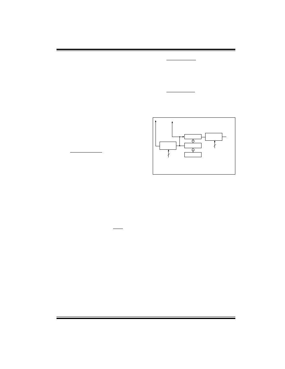
PIC16C72 Series
©
1998 Microchip Technology Inc.
Preliminary
DS39016A-page 31
6.0
TIMER2 MODULE
The Timer2 module timer has the following features:
∑ 8-bit timer (TMR2 register)
∑ 8-bit period register (PR2)
∑ Readable and writable (Both registers)
∑ Software programmable prescaler (1:1, 1:4, 1:16)
∑ Software programmable postscaler (1:1 to 1:16)
∑ Interrupt on TMR2 match of PR2
∑ SSP module optional use of TMR2 output to gen-
erate clock shift
Timer2 has a control register, shown in Figure 6-2.
Timer2 can be shut off by clearing control bit TMR2ON
(T2CON<2>) to minimize power consumption.
Figure 6-1 is a simplified block diagram of the Timer2
module.
Additional information on timer modules is available in
the PICmicroTM Mid-Range MCU Reference Manual,
DS33023.
6.1
Timer2 Operation
Timer2 can be used as the PWM time-base for PWM
mode of the CCP module.
The TMR2 register is readable and writable, and is
cleared on any device reset.
The input clock (F
OSC
/4) has a prescale option of 1:1,
1:4 or 1:16, selected by control bits
T2CKPS1:T2CKPS0 (T2CON<1:0>).
The match output of TMR2 goes through a 4-bit
postscaler (which gives a 1:1 to 1:16 scaling inclusive)
to generate a TMR2 interrupt (latched in flag bit
TMR2IF, (PIR1<1>)).
The prescaler and postscaler counters are cleared
when any of the following occurs:
∑ a write to the TMR2 register
∑ a write to the T2CON register
∑ any device reset (Power-on Reset, MCLR reset,
Watchdog Timer reset, or Brown-out Reset)
TMR2 is not cleared when T2CON is written.
6.2
Timer2 Interrupt
The Timer2 module has an 8-bit period register PR2.
Timer2 increments from 00h until it matches PR2 and
then resets to 00h on the next increment cycle. PR2 is
a readable and writable register. The PR2 register is ini-
tialized to FFh upon reset.
6.3
Output of TMR2
The output of TMR2 (before the postscaler) is fed to the
Synchronous Serial Port module which optionally uses
it to generate shift clock.
FIGURE 6-1:
TIMER2 BLOCK DIAGRAM
Comparator
TMR2
Sets flag
TMR2 reg
output
(1)
Reset
Postscaler
Prescaler
PR2 reg
2
F
OSC
/4
1:1
1:16
1:1, 1:4, 1:16
EQ
4
bit TMR2IF
Note 1:
TMR2 register output can be software selected
by the SSP Module as a baud clock.
to
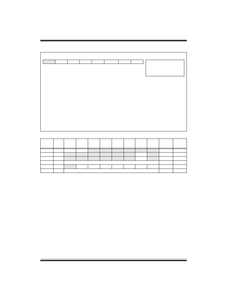
PIC16C72 Series
DS39016A-page 32
Preliminary
©
1998 Microchip Technology Inc.
FIGURE 6-2:
T2CON: TIMER2 CONTROL REGISTER (ADDRESS 12h)
TABLE 6-1
REGISTERS ASSOCIATED WITH TIMER2 AS A TIMER/COUNTER
U-0
R/W-0
R/W-0
R/W-0
R/W-0
R/W-0
R/W-0
R/W-0
--
TOUTPS3 TOUTPS2 TOUTPS1 TOUTPS0 TMR2ON
T2CKPS1 T2CKPS0
R
= Readable bit
W = Writable bit
U
= Unimplemented bit,
read as `0'
- n = Value at POR reset
bit7
bit0
bit 7:
Unimplemented: Read as '0'
bit 6-3:
TOUTPS3:TOUTPS0: Timer2 Output Postscale Select bits
0000
= 1:1 Postscale
0001
= 1:2 Postscale
∑
∑
∑
1111
= 1:16 Postscale
bit 2:
TMR2ON: Timer2 On bit
1 = Timer2 is on
0 = Timer2 is off
bit 1-0:
T2CKPS1:T2CKPS0: Timer2 Clock Prescale Select bits
00
= Prescaler is 1
01
= Prescaler is 4
1x
= Prescaler is 16
Address
Name
Bit 7
Bit 6
Bit 5
Bit 4
Bit 3
Bit 2
Bit 1
Bit 0
Value on:
POR,
BOR
Value on
all other
resets
0Bh,8Bh
INTCON
GIE
PEIE
T0IE
INTE
RBIE
T0IF
INTF
RBIF
0000 000x
0000 000u
0Ch
PIR1
(1)
ADIF
(1)
(1)
SSPIF
CCP1IF
TMR2IF
TMR1IF
0000 0000
0000 0000
8Ch
PIE1
(1)
ADIE
(1)
(1)
SSPIE
CCP1IE
TMR2IE
TMR1IE
0000 0000
0000 0000
11h
TMR2
Timer2 module's register
0000 0000
0000 0000
12h
T2CON
--
TOUTPS3 TOUTPS2 TOUTPS1 TOUTPS0 TMR2ON
T2CKPS1
T2CKPS0
-000 0000
-000 0000
92h
PR2
Timer2 Period Register
1111 1111
1111 1111
Legend:
x
= unknown,
u
= unchanged,
-
= unimplemented read as '0'. Shaded cells are not used by the Timer2 module.
2:
These bits are unimplemented, read as '0'.

PIC16C72 Series
©
1998 Microchip Technology Inc.
Preliminary
DS39016A-page 33
7.0
CAPTURE/COMPARE/PWM
(CCP) MODULE
The CCP (Capture/Compare/PWM) module contains a
16-bit register which can operate as a 16-bit capture
register, as a 16-bit compare register or as a PWM
master/slave Duty Cycle register. Table 7-1 shows the
timer resources of the CCP module modes.
Capture/Compare/PWM Register1 (CCPR1) is com-
prised of two 8-bit registers: CCPR1L (low byte) and
CCPR1H (high byte). The CCP1CON register controls
the operation of CCP1. All are readable and writable.
Additional information on the CCP module is available
in the PICmicroTM Mid-Range MCU Reference Manual,
DS33023.
TABLE 7-1
CCP MODE - TIMER
RESOURCE
FIGURE 7-1:
CCP1CON REGISTER (ADDRESS 17h)
CCP Mode
Timer Resource
Capture
Compare
PWM
Timer1
Timer1
Timer2
U-0
U-0
R/W-0
R/W-0
R/W-0
R/W-0
R/W-0
R/W-0
--
--
CCP1X
CCP1Y CCP1M3
CCP1M2
CCP1M1 CCP1M0
R = Readable bit
W = Writable bit
U = Unimplemented bit,
read as `0'
- n =Value at POR reset
bit7
bit0
bit 7-6:
Unimplemented: Read as '0'
bit 5-4: CCP1X:CCP1Y: PWM Least Significant bits
Capture Mode: Unused
Compare Mode: Unused
PWM Mode: These bits are the two LSbs of the PWM duty cycle. The eight MSbs are found in CCPR1L.
bit 3-0: CCP1M3:CCP1M0: CCP1 Mode Select bits
0000
= Capture/Compare/PWM off (resets CCP1 module)
0100
= Capture mode, every falling edge
0101
= Capture mode, every rising edge
0110
= Capture mode, every 4th rising edge
0111
= Capture mode, every 16th rising edge
1000
= Compare mode, set output on match (CCP1IF bit is set)
1001
= Compare mode, clear output on match (CCP1IF bit is set)
1010
= Compare mode, generate software interrupt on match (CCP1IF bit is set, CCP1 pin is unaffected)
1011
= Compare mode, trigger special event (CCP1IF bit is set; CCP1 resets TMR1 and starts an A/D
conversion (if A/D module is enabled))
11xx
= PWM mode
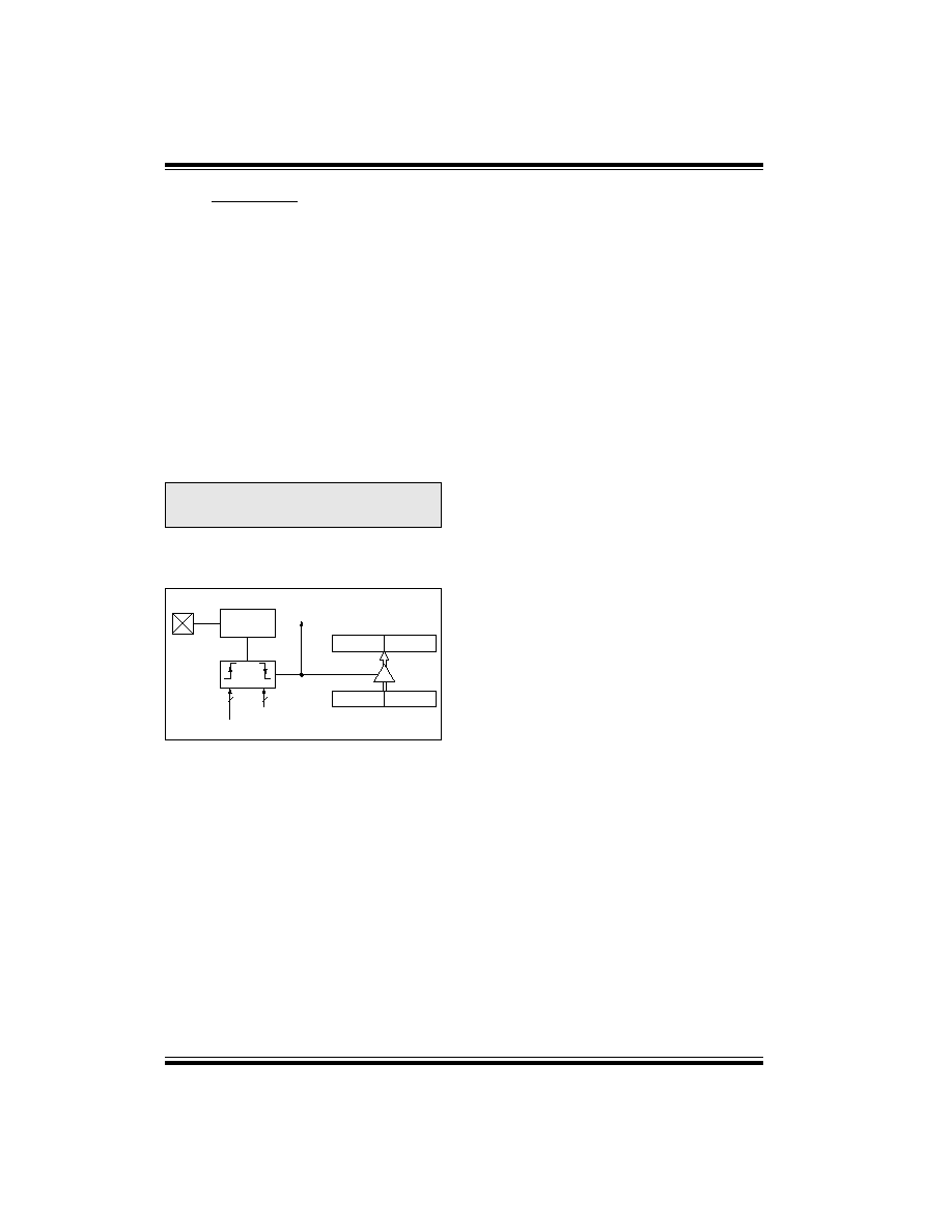
PIC16C72 Series
DS39016A-page 34
Preliminary
©
1998 Microchip Technology Inc.
7.1
Capture Mode
In Capture mode, CCPR1H:CCPR1L captures the
16-bit value of the TMR1 register when an event occurs
on pin RC2/CCP1. An event is defined as:
∑ every falling edge
∑ every rising edge
∑ every 4th rising edge
∑ every 16th rising edge
An event is selected by control bits CCP1M3:CCP1M0
(CCP1CON<3:0>). When a capture is made, the inter-
rupt request flag bit CCP1IF (PIR1<2>) is set. It must
be cleared in software. If another capture occurs before
the value in register CCPR1 is read, the old captured
value will be lost.
7.1.1
CCP PIN CONFIGURATION
In Capture mode, the RC2/CCP1 pin should be config-
ured as an input by setting the TRISC<2> bit.
FIGURE 7-2:
CAPTURE MODE
OPERATION BLOCK
DIAGRAM
7.1.2
TIMER1 MODE SELECTION
Timer1 must be running in timer mode or synchronized
counter mode for the CCP module to use the capture
feature. In asynchronous counter mode, the capture
operation may not work.
7.1.3
SOFTWARE INTERRUPT
When the Capture mode is changed, a false capture
interrupt may be generated. The user should keep bit
CCP1IE (PIE1<2>) clear to avoid false interrupts and
should clear the flag bit CCP1IF following any such
change in operating mode.
7.1.4
CCP PRESCALER
There are four prescaler settings, specified by bits
CCP1M3:CCP1M0. Whenever the CCP module is
turned off, or the CCP module is not in capture mode,
the prescaler counter is cleared. This means that any
reset will clear the prescaler counter.
Switching from one capture prescaler to another may
generate an interrupt. Also, the prescaler counter will
not be cleared, therefore the first capture may be from
a non-zero prescaler. Example 7-1 shows the recom-
mended method for switching between capture pres-
calers. This example also clears the prescaler counter
and will not generate the "false" interrupt.
EXAMPLE 7-1:
CHANGING BETWEEN
CAPTURE PRESCALERS
CLRF CCP1CON ;Turn CCP module off
MOVLW NEW_CAPT_PS ;Load the W reg with
; the new prescaler
; mode value and CCP ON
MOVWF CCP1CON ;Load CCP1CON with this
; value
Note:
If the RC2/CCP1 is configured as an out-
put, a write to the port can cause a capture
condition.
CCPR1H
CCPR1L
TMR1H
TMR1L
Set flag bit CCP1IF
(PIR1<2>)
Capture
Enable
Q's
CCP1CON<3:0>
RC2/CCP1
Prescaler
˜
1, 4, 16
and
edge detect
Pin
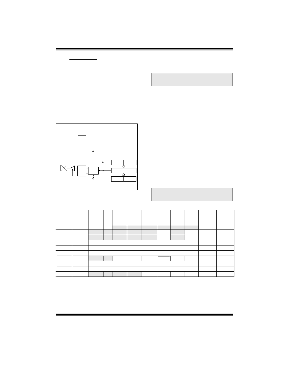
PIC16C72 Series
©
1998 Microchip Technology Inc.
Preliminary
DS39016A-page 35
7.2
Compare Mode
In Compare mode, the 16-bit CCPR1 register value is
constantly compared against the TMR1 register pair
value. When a match occurs, the RC2/CCP1 pin is:
∑ driven High
∑ driven Low
∑ remains Unchanged
The action on the pin is based on the value of control
bits CCP1M3:CCP1M0 (CCP1CON<3:0>). At the
same time, interrupt flag bit CCP1IF is set.
FIGURE 7-3:
COMPARE MODE
OPERATION BLOCK
DIAGRAM
7.2.1
CCP PIN CONFIGURATION
The user must configure the RC2/CCP1 pin as an out-
put by clearing the TRISC<2> bit.
7.2.2
TIMER1 MODE SELECTION
Timer1 must be running in Timer mode or Synchro-
nized Counter mode if the CCP module is using the
compare feature. In Asynchronous Counter mode, the
compare operation may not work.
7.2.3
SOFTWARE INTERRUPT MODE
When generate software interrupt is chosen the CCP1
pin is not affected. Only a CCP interrupt is generated (if
enabled).
7.2.4
SPECIAL EVENT TRIGGER
In this mode, an internal hardware trigger is generated
which may be used to initiate an action.
The special event trigger output of CCP1 resets the
TMR1 register pair. This allows the CCPR1 register to
effectively be a 16-bit programmable period register for
Timer1.
The special trigger output of CCP1 resets the TMR1
register pair, and starts an A/D conversion (if the A/D
module is enabled).
TABLE 7-2
REGISTERS ASSOCIATED WITH CAPTURE, COMPARE, AND TIMER1
CCPR1H CCPR1L
TMR1H
TMR1L
Comparator
Q
S
R
Output
Logic
Special Event Trigger
Set flag bit CCP1IF
(PIR1<2>)
match
RC2/CCP1
TRISC<2>
CCP1CON<3:0>
Mode Select
Output Enable
Pin
Special event trigger will:
reset Timer1, but not set interrupt flag bit TMR1IF (PIR1<0>),
and set bit GO/DONE (ADCON0<2>)
which starts an A/D conversion
Note:
Clearing the CCP1CON register will force
the RC2/CCP1 compare output latch to the
default low level. This is not the data latch.
Note:
The special event trigger from the CCP1
module will not set interrupt flag bit
TMR1IF (PIR1<0>).
Address
Name
Bit 7
Bit 6
Bit 5
Bit 4
Bit 3
Bit 2
Bit 1
Bit 0
Value on:
POR,
BOR
Value on
all other
resets
0Bh,8Bh
INTCON
GIE
PEIE
T0IE
INTE
RBIE
T0IF
INTF
RBIF
0000 000x 0000 000u
0Ch
PIR1
(1)
ADIF
(1)
(1)
SSPIF
CCP1IF
TMR2IF
TMR1IF
0000 0000 0000 0000
8Ch
PIE1
(1)
ADIE
(1)
(1)
SSPIE
CCP1IE
TMR2IE
TMR1IE
0000 0000 0000 0000
87h
TRISC
PORTC Data Direction Register
1111 1111 1111 1111
0Eh
TMR1L
Holding register for the Least Significant Byte of the 16-bit TMR1 register
xxxx xxxx uuuu uuuu
0Fh
TMR1H
Holding register for the Most Significant Byte of the 16-bit TMR1register
xxxx xxxx uuuu uuuu
10h
T1CON
--
--
T1CKPS1 T1CKPS0 T1OSCEN T1SYNC TMR1CS TMR1ON
--00 0000 --uu uuuu
15h
CCPR1L
Capture/Compare/PWM register1 (LSB)
xxxx xxxx uuuu uuuu
16h
CCPR1H
Capture/Compare/PWM register1 (MSB)
xxxx xxxx uuuu uuuu
17h
CCP1CON
--
--
CCP1X
CCP1Y
CCP1M3
CCP1M2 CCP1M1 CCP1M0
--00 0000 --00 0000
Legend:
x
= unknown,
u
= unchanged,
-
= unimplemented read as '0'. Shaded cells are not used by Capture and Timer1.
Note 1:
These bits/registers are unimplemented, read as '0'.
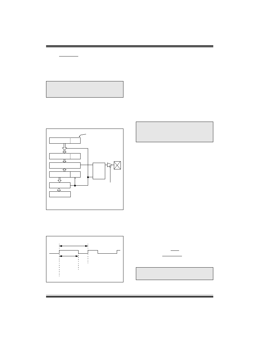
PIC16C72 Series
DS39016A-page 36
Preliminary
©
1998 Microchip Technology Inc.
7.3
PWM Mode
In Pulse Width Modulation (PWM) mode, the CCP1 pin
produces up to a 10-bit resolution PWM output. Since
the CCP1 pin is multiplexed with the PORTC data latch,
the TRISC<2> bit must be cleared to make the CCP1
pin an output.
Figure 7-4 shows a simplified block diagram of the CCP
module in PWM mode.
For a step by step procedure on how to set up the CCP
module for PWM operation, see Section 7.3.3.
FIGURE 7-4:
SIMPLIFIED PWM BLOCK
DIAGRAM
A PWM output (Figure 7-5) has a time base (period)
and a time that the output stays high (duty cycle). The
frequency of the PWM is the inverse of the period
(1/period).
FIGURE 7-5:
PWM OUTPUT
7.3.1
PWM PERIOD
The PWM period is specified by writing to the PR2 reg-
ister. The PWM period can be calculated using the fol-
lowing formula:
PWM period = [(PR2) + 1] • 4 • T
OSC
•
(TMR2 prescale value)
PWM frequency is defined as 1 / [PWM period].
When TMR2 is equal to PR2, the following three events
occur on the next increment cycle:
∑ TMR2 is cleared
∑ The CCP1 pin is set (exception: if PWM duty
cycle = 0%, the CCP1 pin will not be set)
∑ The PWM duty cycle is latched from CCPR1L into
CCPR1H
7.3.2
PWM DUTY CYCLE
The PWM duty cycle is specified by writing to the
CCPR1L register and to the CCP1CON<5:4> bits. Up
to 10-bit resolution is available: the CCPR1L contains
the eight MSbs and the CCP1CON<5:4> contains the
two LSbs. This 10-bit value is represented by
CCPR1L:CCP1CON<5:4>. The following equation is
used to calculate the PWM duty cycle in time:
PWM duty cycle = (CCPR1L:CCP1CON<5:4>) •
Tosc • (TMR2 prescale value)
CCPR1L and CCP1CON<5:4> can be written to at any
time, but the duty cycle value is not latched into
CCPR1H until after a match between PR2 and TMR2
occurs (i.e., the period is complete). In PWM mode,
CCPR1H is a read-only register.
The CCPR1H register and a 2-bit internal latch are
used to double buffer the PWM duty cycle. This double
buffering is essential for glitchless PWM operation.
When the CCPR1H and 2-bit latch match TMR2 con-
catenated with an internal 2-bit Q clock or 2 bits of the
TMR2 prescaler, the CCP1 pin is cleared.
Maximum PWM resolution (bits) for a given PWM
frequency:
Note:
Clearing the CCP1CON register will force
the CCP1 PWM output latch to the default
low level. This is not the PORTC I/O data
latch.
CCPR1L
CCPR1H (Slave)
Comparator
TMR2
Comparator
PR2
(Note 1)
R
Q
S
Duty cycle registers
CCP1CON<5:4>
Clear Timer,
CCP1 pin and
latch D.C.
TRISC<2>
RC2/CCP1
Note 1: 8-bit timer is concatenated with 2-bit internal Q clock
or 2 bits of the prescaler to create 10-bit time-base.
Period
Duty Cycle
TMR2 = PR2
TMR2 = Duty Cycle
TMR2 = PR2
Note:
The Timer2 postscaler (see Section 6.0) is
not used in the determination of the PWM
frequency. The postscaler could be used to
have a servo update rate at a different fre-
quency than the PWM output.
Note:
If the PWM duty cycle value is longer than
the PWM period the CCP1 pin will not be
cleared.
log
(
F
PWM
log(2)
F
OSC
)
bits
=
PIC16C72 Series
©
1998 Microchip Technology Inc.
Preliminary
DS39016A-page 37
For an example PWM period and duty cycle calcula-
tion, see the PICmicroTM Mid-Range MCU Reference
Manual (DS33023).
7.3.3
SET-UP FOR PWM OPERATION
The following steps should be taken when configuring
the CCP module for PWM operation:
1.
Set the PWM period by writing to the PR2 regis-
ter.
2.
Set the PWM duty cycle by writing to the
CCPR1L register and CCP1CON<5:4> bits.
3.
Make the CCP1 pin an output by clearing the
TRISC<2> bit.
4.
Set the TMR2 prescale value and enable Timer2
by writing to T2CON.
5.
Configure the CCP1 module for PWM operation.
TABLE 7-3
EXAMPLE PWM FREQUENCIES AND RESOLUTIONS AT 20 MHz
TABLE 7-4
REGISTERS ASSOCIATED WITH PWM AND TIMER2
PWM Frequency
1.22 kHz
4.88 kHz
19.53 kHz
78.12 kHz
156.3 kHz
208.3 kHz
Timer Prescaler (1, 4, 16)
16
4
1
1
1
1
PR2 Value
0xFF
0xFF
0xFF
0x3F
0x1F
0x17
Maximum Resolution (bits)
10
10
10
8
7
5.5
Address
Name
Bit 7
Bit 6
Bit 5
Bit 4
Bit 3
Bit 2
Bit 1
Bit 0
Value on:
POR,
BOR
Value on
all other
resets
0Bh,8Bh
INTCON
GIE
PEIE
T0IE
INTE
RBIE
T0IF
INTF
RBIF
0000 000x 0000 000u
0Ch
PIR1
(1)
ADIF
(1)
(1)
SSPIF
CCP1IF
TMR2IF
TMR1IF
0000 0000 0000 0000
8Ch
PIE1
(1)
ADIE
(1)
(1)
SSPIE
CCP1IE
TMR2IE
TMR1IE
0000 0000 0000 0000
87h
TRISC
PORTC Data Direction Register
1111 1111 1111 1111
11h
TMR2
Timer2 module's register
0000 0000 0000 0000
92h
PR2
Timer2 module's period register
1111 1111 1111 1111
12h
T2CON
--
TOUTPS
3
TOUTPS
2
TOUTPS
1
TOUTPS
0
TMR2O
N
T2CKPS
1
T2CKPS
0
-000 0000 -000 0000
15h
CCPR1L
Capture/Compare/PWM register1 (LSB)
xxxx xxxx uuuu uuuu
16h
CCPR1H
Capture/Compare/PWM register1 (MSB)
xxxx xxxx uuuu uuuu
17h
CCP1CON
--
--
CCP1X
CCP1Y
CCP1M3 CCP1M2 CCP1M1 CCP1M0
--00 0000 --00 0000
Legend:
x
= unknown,
u
= unchanged,
-
= unimplemented read as '0'. Shaded cells are not used by PWM and Timer2.
Note 1:
These bits/registers are unimplemented, read as '0'.

PIC16C72 Series
DS39016A-page 38
Preliminary
©
1998 Microchip Technology Inc.
NOTES:

PIC16C72 Series
©
1998 Microchip Technology Inc.
Preliminary
DS39016A-page 39
8.0
SYNCHRONOUS SERIAL
PORT (SSP) MODULE
8.1
SSP Module Overview
The Synchronous Serial Port (SSP) module is a serial
interface useful for communicating with other periph-
eral or microcontroller devices. These peripheral
devices may be Serial EEPROMs, shift registers, dis-
play drivers, A/D converters, etc. The SSP module can
operate in one of two modes:
∑ Serial Peripheral Interface (SPI)
∑ Inter-Integrated Circuit (I
2
C)
The SSP module in I
2
C mode works the same in all
PIC16C72 series devices that have an SSP module.
However the SSP Module in SPI mode has differences
between the PIC16C72 and the PIC16CR72 device.
The register definitions and operational description of
SPI mode has been split into two sections because of
the differences between the PIC16C72 and the
PIC16CR72 device. The default reset values of both
the SPI modules is the same regardless of the device:
8.2
SPI Mode for PIC16C72 .................................. 40
8.3
SPI Mode for PIC16CR72 ............................... 43
8.4
SSP I
2
C Operation .......................................... 47
For an I
2
C Overview, refer to the PICmicroTM Mid-
Range MCU Reference Manual (DS33023). Also, refer
to Application Note AN578,
"Use of the SSP Module in
the I
2
C Multi-Master Environment."
PIC16C72 Series
DS39016A-page 40
Preliminary
©
1998 Microchip Technology Inc.
8.2
SPI Mode for PIC16C72
This section contains register definitions and opera-
tional characteristics of the SPI module on the
PIC16C72 device only.
Additional information on SPI operation may be found
in the PICmicroTM Mid-Range MCU Reference Manual,
DS33023.
FIGURE 8-1:
SSPSTAT: SYNC SERIAL PORT STATUS REGISTER
(ADDRESS 94h) (PIC16C72)
U-0
U-0
R-0
R-0
R-0
R-0
R-0
R-0
--
--
D/A
P
S
R/W
UA
BF
R = Readable bit
W = Writable bit
U = Unimplemented bit,
read as `0'
- n =Value at POR reset
bit7
bit0
bit 7-6:
Unimplemented: Read as '0'
bit 5:
D/A: Data/Address bit (I
2
C mode only)
1 = Indicates that the last byte received or transmitted was data
0 = Indicates that the last byte received or transmitted was address
bit 4:
P: Stop bit (I
2
C mode only. This bit is cleared when the SSP module is disabled, SSPEN is cleared)
1 = Indicates that a stop bit has been detected last (this bit is '0' on RESET)
0 = Stop bit was not detected last
bit 3:
S: Start bit (I
2
C mode only. This bit is cleared when the SSP module is disabled, SSPEN is cleared)
1 = Indicates that a start bit has been detected last (this bit is '0' on RESET)
0 = Start bit was not detected last
bit 2:
R/W: Read/Write bit information (I
2
C mode only)
This bit holds the R/W bit information following the last address match. This bit is valid from the address
match to the next start bit, stop bit, or ACK bit.
1 = Read
0 = Write
bit 1:
UA: Update Address (10-bit I
2
C mode only)
1 = Indicates that the user needs to update the address in the SSPADD register
0 = Address does not need to be updated
bit 0:
BF: Buffer Full Status bit
Receive (SPI and I
2
C modes)
1 = Receive complete, SSPBUF is full
0 = Receive not complete, SSPBUF is empty
Transmit (I
2
C mode only)
1 = Transmit in progress, SSPBUF is full
0 = Transmit complete, SSPBUF is empty
PIC16C72 Series
©
1998 Microchip Technology Inc.
Preliminary
DS39016A-page 41
FIGURE 8-2:
SSPCON: SYNC SERIAL PORT CONTROL REGISTER (ADDRESS 14h) (PIC16C72)
R/W-0
R/W-0
R/W-0
R/W-0
R/W-0
R/W-0
R/W-0
R/W-0
WCOL
SSPOV
SSPEN
CKP
SSPM3
SSPM2
SSPM1
SSPM0
R = Readable bit
W = Writable bit
U = Unimplemented bit,
read as `0'
- n =Value at POR reset
bit7
bit0
bit 7:
WCOL: Write Collision Detect bit
1 = The SSPBUF register is written while it is still transmitting the previous word
(must be cleared in software)
0 = No collision
bit 6:
SSPOV: Receive Overflow Detect bit
In SPI mode
1 = A new byte is received while the SSPBUF register is still holding the previous data. In case of over-
flow, the data in SSPSR register is lost. Overflow can only occur in slave mode. The user must read the
SSPBUF, even if only transmitting data, to avoid setting overflow. In master operation, the overflow bit is
not set since each new reception (and transmission) is initiated by writing to the SSPBUF register.
0 = No overflow
In I
2
C mode
1 = A byte is received while the SSPBUF register is still holding the previous byte. SSPOV is a "don't
care" in transmit mode. SSPOV must be cleared in software in either mode.
0 = No overflow
bit 5:
SSPEN: Synchronous Serial Port Enable bit
In SPI mode
1 = Enables serial port and configures SCK, SDO, and SDI as serial port pins
0 = Disables serial port and configures these pins as I/O port pins
In I
2
C mode
1 = Enables the serial port and configures the SDA and SCL pins as serial port pins
0 = Disables serial port and configures these pins as I/O port pins
In both modes, when enabled, these pins must be properly configured as input or output.
bit 4:
CKP: Clock Polarity Select bit
In SPI mode
1 = Idle state for clock is a high level. Transmit happens on falling edge, receive on rising edge.
0 = Idle state for clock is a low level. Transmit happens on rising edge, receive on falling edge.
In I
2
C mode
SCK release control
1 = Enable clock
0 = Holds clock low (clock stretch) (Used to ensure data setup time)
bit 3-0: SSPM3:SSPM0: Synchronous Serial Port Mode Select bits
0000
= SPI master operation, clock = Fosc/4
0001
= SPI master operation, clock = Fosc/16
0010
= SPI master operation, clock = Fosc/64
0011
= SPI master operation, clock = TMR2 output/2
0100
= SPI slave mode, clock = SCK pin. SS pin control enabled.
0101
= SPI slave mode, clock = SCK pin. SS pin control disabled. SS can be used as I/O pin.
0110
= I
2
C slave mode, 7-bit address
0111
= I
2
C slave mode, 10-bit address
1011
= I
2
C firmware controlled master operation (slave idle)
1110
= I
2
C slave mode, 7-bit address with start and stop bit interrupts enabled
1111
= I
2
C slave mode, 10-bit address with start and stop bit interrupts enabled
PIC16C72 Series
DS39016A-page 42
Preliminary
©
1998 Microchip Technology Inc.
8.2.1
OPERATION OF SSP MODULE IN SPI
MODE - PIC16C72
A block diagram of the SSP Module in SPI Mode is
shown in Figure 8-3.
The SPI mode allows 8-bits of data to be synchro-
nously transmitted and received simultaneously. To
accomplish communication, typically three pins are
used:
∑ Serial Data Out (SDO)
RC5/SDO
∑ Serial Data In (SDI)
RC4/SDI/SDA
∑ Serial Clock (SCK)
RC3/SCK/SCL
Additionally a fourth pin may be used when in a slave
mode of operation:
∑ Slave Select (SS)
RA5/SS/AN4
When initializing the SPI, several options need to be
specified. This is done by programming the appropriate
control bits in the SSPCON register (SSPCON<5:0>).
These control bits allow the following to be specified:
∑ Master Operation (SCK is the clock output)
∑ Slave Mode (SCK is the clock input)
∑ Clock Polarity (Output/Input data on the Rising/
Falling edge of SCK)
∑ Clock Rate (master operation only)
∑ Slave Select Mode (Slave mode only)
To enable the serial port, SSP enable bit SSPEN
(SSPCON<5>) must be set. To reset or reconfigure SPI
mode, clear enable bit SSPEN, re-initialize SSPCON
register, and then set enable bit SSPEN. This config-
ures the SDI, SDO, SCK, and SS pins as serial port
pins. For the pins to behave as the serial port function,
they must have their data direction bits (in the TRIS reg-
ister) appropriately programmed. That is:
∑ SDI must have TRISC<4> set
∑ SDO must have TRISC<5> cleared
∑ SCK (master operation) must have TRISC<3>
cleared
∑ SCK (Slave mode) must have TRISC<3> set
∑ SS must have TRISA<5> set (if implemented)
FIGURE 8-3:
SSP BLOCK DIAGRAM
(SPI MODE)
TABLE 8-1
REGISTERS ASSOCIATED WITH SPI OPERATION
Read
Write
Internal
data bus
RC4/SDI/SDA
RC5/SDO
RA5/SS/AN4
RC3/SCK/
SSPSR reg
SSPBUF reg
SSPM3:SSPM0
bit0
shift
clock
SS Control
Enable
Edge
Select
Clock Select
TMR2 output
T
CY
Prescaler
4, 16, 64
TRISC<3>
2
Edge
Select
2
4
SCL
Address
Name
Bit 7
Bit 6
Bit 5
Bit 4
Bit 3
Bit 2
Bit 1
Bit 0
Value on:
POR,
BOR
Value on
all other
resets
0Bh,8Bh
INTCON
GIE
PEIE
T0IE
INTE
RBIE
T0IF
INTF
RBIF
0000 000x
0000 000u
0Ch
PIR1
(1)
ADIF
(1)
(1)
SSPIF
CCP1IF TMR2IF TMR1IF
0000 0000
0000 0000
8Ch
PIE1
(1)
ADIE
(1)
(1)
SSPIE
CCP1IE TMR2IE TMR1IE
0000 0000
0000 0000
87h
TRISC
PORTC Data Direction Register
1111 1111
1111 1111
13h
SSPBUF
Synchronous Serial Port Receive Buffer/Transmit Register
xxxx xxxx
uuuu uuuu
14h
SSPCON
WCOL
SSPOV SSPEN
CKP
SSPM3 SSPM2
SSPM1
SSPM0
0000 0000
0000 0000
85h
TRISA
--
--
PORTA Data Direction Register
--11 1111
--11 1111
94h
SSP-
STAT
--
--
D/A
P
S
R/W
UA
BF
--00 0000
--00 0000
Legend:
x
= unknown,
u
= unchanged,
-
= unimplemented read as '0'. Shaded cells are not used by the SSP in SPI mode.
Note 1:
These bits are unimplemented, read as '0'.
PIC16C72 Series
©
1998 Microchip Technology Inc.
Preliminary
DS39016A-page 43
8.3
SPI Mode for PIC16CR72
This section contains register definitions and opera-
tional characteristics of the SPI module on the
PIC16CR72
device only.
Additional information on SPI operation may be found
in the PICmicroTM Mid-Range MCU Reference Manual,
DS33023.
FIGURE 8-4:
SSPSTAT: SYNC SERIAL PORT STATUS REGISTER
(ADDRESS 94h) (PIC16CR72)
R/W-0 R/W-0
R-0
R-0
R-0
R-0
R-0
R-0
SMP
CKE
D/A
P
S
R/W
UA
BF
R = Readable bit
W = Writable bit
U = Unimplemented bit,
read as `0'
- n =Value at POR reset
bit7
bit0
bit 7:
SMP: SPI data input sample phase
SPI Master Operation
1 = Input data sampled at end of data output time
0 = Input data sampled at middle of data output time
SPI Slave Mode
SMP must be cleared when SPI is used in slave mode
bit 6:
CKE: SPI Clock Edge Select
CKP = 0
1 = Data transmitted on rising edge of SCK
0 = Data transmitted on falling edge of SCK
CKP = 1
1 = Data transmitted on falling edge of SCK
0 = Data transmitted on rising edge of SCK
bit 5:
D/A: Data/Address bit (I
2
C mode only)
1 = Indicates that the last byte received or transmitted was data
0 = Indicates that the last byte received or transmitted was address
bit 4:
P: Stop bit (I
2
C mode only. This bit is cleared when the SSP module is disabled, or when the Start bit is
detected last, SSPEN is cleared)
1 = Indicates that a stop bit has been detected last (this bit is '0' on RESET)
0 = Stop bit was not detected last
bit 3:
S: Start bit (I
2
C mode only. This bit is cleared when the SSP module is disabled, or when the Stop bit is
detected last, SSPEN is cleared)
1 = Indicates that a start bit has been detected last (this bit is '0' on RESET)
0 = Start bit was not detected last
bit 2:
R/W: Read/Write bit information (I
2
C mode only)
This bit holds the R/W bit information following the last address match. This bit is only valid from the
address match to the next start bit, stop bit, or ACK bit.
1 = Read
0 = Write
bit 1:
UA: Update Address (10-bit I
2
C mode only)
1 = Indicates that the user needs to update the address in the SSPADD register
0 = Address does not need to be updated
bit 0:
BF: Buffer Full Status bit
Receive (SPI and I
2
C modes)
1 = Receive complete, SSPBUF is full
0 = Receive not complete, SSPBUF is empty
Transmit (I
2
C mode only)
1 = Transmit in progress, SSPBUF is full
0 = Transmit complete, SSPBUF is empty
PIC16C72 Series
DS39016A-page 44
Preliminary
©
1998 Microchip Technology Inc.
FIGURE 8-5:
SSPCON: SYNC SERIAL PORT CONTROL REGISTER (ADDRESS 14h) (PIC16CR72)
R/W-0
R/W-0
R/W-0
R/W-0
R/W-0
R/W-0
R/W-0
R/W-0
WCOL
SSPOV
SSPEN
CKP
SSPM3
SSPM2
SSPM1
SSPM0
R = Readable bit
W = Writable bit
U = Unimplemented bit,
read as `0'
- n =Value at POR reset
bit7
bit0
bit 7:
WCOL: Write Collision Detect bit
1 = The SSPBUF register is written while it is still transmitting the previous word
(must be cleared in software)
0 = No collision
bit 6:
SSPOV: Receive Overflow Indicator bit
In SPI mode
1 = A new byte is received while the SSPBUF register is still holding the previous data. In case of over-
flow, the data in SSPSR is lost. Overflow can only occur in slave mode. The user must read the SSPBUF,
even if only transmitting data, to avoid setting overflow. In master operation, the overflow bit is not set
since each new reception (and transmission) is initiated by writing to the SSPBUF register.
0 = No overflow
In I
2
C mode
1 = A byte is received while the SSPBUF register is still holding the previous byte. SSPOV is a "don't
care" in transmit mode. SSPOV must be cleared in software in either mode.
0 = No overflow
bit 5:
SSPEN: Synchronous Serial Port Enable bit
In SPI mode
1 = Enables serial port and configures SCK, SDO, and SDI as serial port pins
0 = Disables serial port and configures these pins as I/O port pins
In I
2
C mode
1 = Enables the serial port and configures the SDA and SCL pins as serial port pins
0 = Disables serial port and configures these pins as I/O port pins
In both modes, when enabled, these pins must be properly configured as input or output.
bit 4:
CKP: Clock Polarity Select bit
In SPI mode
1 = Idle state for clock is a high level
0 = Idle state for clock is a low level
In I
2
C mode
SCK release control
1 = Enable clock
0 = Holds clock low (clock stretch) (Used to ensure data setup time)
bit 3-0: SSPM3:SSPM0: Synchronous Serial Port Mode Select bits
0000
= SPI master operation, clock = F
OSC
/4
0001
= SPI master operation, clock = F
OSC
/16
0010
= SPI master operation, clock = F
OSC
/64
0011
= SPI master operation, clock = TMR2 output/2
0100
= SPI slave mode, clock = SCK pin. SS pin control enabled.
0101
= SPI slave mode, clock = SCK pin. SS pin control disabled. SS can be used as I/O pin
0110
= I
2
C slave mode, 7-bit address
0111
= I
2
C slave mode, 10-bit address
1011
= I
2
C firmware controlled master operation (slave idle)
1110
= I
2
C slave mode, 7-bit address with start and stop bit interrupts enabled
1111
= I
2
C slave mode, 10-bit address with start and stop bit interrupts enabled
PIC16C72 Series
©
1998 Microchip Technology Inc.
Preliminary
DS39016A-page 45
8.3.1
OPERATION OF SSP MODULE IN SPI
MODE - PIC16CR72
A block diagram of the SSP Module in SPI Mode is
shown in Figure 8-6.
The SPI mode allows 8-bits of data to be synchro-
nously transmitted and received simultaneously. To
accomplish communication, typically three pins are
used:
∑ Serial Data Out (SDO)
RC5/SDO
∑ Serial Data In (SDI)
RC4/SDI/SDA
∑ Serial Clock (SCK)
RC3/SCK/SCL
Additionally a fourth pin may be used when in a slave
mode of operation:
∑ Slave Select (SS)
RA5/SS/AN4
When initializing the SPI, several options need to be
specified. This is done by programming the appropriate
control bits in the SSPCON register (SSPCON<5:0>)
and SSPSTAT<7:6>. These control bits allow the fol-
lowing to be specified:
∑ Master Operation (SCK is the clock output)
∑ Slave Mode (SCK is the clock input)
∑ Clock Polarity (Idle state of SCK)
∑ Clock Edge (Output data on rising/falling edge of
SCK)
∑ Clock Rate (master operation only)
∑ Slave Select Mode (Slave mode only)
To enable the serial port, SSP Enable bit, SSPEN
(SSPCON<5>) must be set. To reset or reconfigure SPI
mode, clear bit SSPEN, re-initialize the SSPCON reg-
ister, and then set bit SSPEN. This configures the SDI,
SDO, SCK, and SS pins as serial port pins. For the pins
to behave as the serial port function, they must have
their data direction bits (in the TRISC register) appro-
priately programmed. That is:
∑ SDI must have TRISC<4> set
∑ SDO must have TRISC<5> cleared
∑ SCK (master operation) must have TRISC<3>
cleared
∑ SCK (Slave mode) must have TRISC<3> set
∑ SS must have TRISA<5> set
FIGURE 8-6:
SSP BLOCK DIAGRAM
(SPI MODE)(PIC16CR72)
Note:
When the SPI is in Slave Mode with SS pin
control enabled, (SSPCON<3:0> =
0100
)
the SPI module will reset if the SS pin is set
to V
DD
.
Note:
If the SPI is used in Slave Mode with
CKE = '1', then the SS pin control must be
enabled.
Read
Write
Internal
data bus
RC4/SDI/SDA
RC5/SDO
RA5/SS/AN4
RC3/SCK/
SSPSR reg
SSPBUF reg
SSPM3:SSPM0
bit0
shift
clock
SS Control
Enable
Edge
Select
Clock Select
TMR2 output
T
CY
Prescaler
4, 16, 64
TRISC<3>
2
Edge
Select
2
4
SCL
PIC16C72 Series
DS39016A-page 46
Preliminary
©
1998 Microchip Technology Inc.
TABLE 8-2
REGISTERS ASSOCIATED WITH SPI OPERATION (PIC16CR72)
Address
Name
Bit 7
Bit 6
Bit 5
Bit 4
Bit 3
Bit 2
Bit 1
Bit 0
Value on:
POR,
BOR
Value on
all other
resets
0Bh,8Bh
INTCON
GIE
PEIE
T0IE
INTE
RBIE
T0IF
INTF
RBIF
0000 000x
0000 000u
0Ch
PIR1
(1)
ADIF
(1)
(1)
SSPIF
CCP1IF
TMR2IF TMR1IF
0000 0000
0000 0000
8Ch
PIE1
(1)
ADIE
(1)
(1)
SSPIE
CCP1IE TMR2IE TMR1IE
0000 0000
0000 0000
87h
TRISC
PORTC Data Direction Register
1111 1111
1111 1111
13h
SSPBUF
Synchronous Serial Port Receive Buffer/Transmit Register
xxxx xxxx
uuuu uuuu
14h
SSPCON
WCOL
SSPOV SSPEN
CKP
SSPM3
SSPM2
SSPM1
SSPM0
0000 0000
0000 0000
85h
TRISA
--
--
PORTA Data Direction Register
--11 1111
--11 1111
94h
SSPSTAT
SMP
CKE
D/A
P
S
R/W
UA
BF
0000 0000
0000 0000
Legend:
x
= unknown,
u
= unchanged,
-
= unimplemented read as '0'. Shaded cells are not used by the SSP in SPI mode.
Note 1:
Always maintain these bits clear.
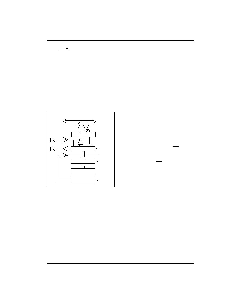
PIC16C72 Series
©
1998 Microchip Technology Inc.
Preliminary
DS39016A-page 47
8.4
SSP I
2
C Operation
The SSP module in I
2
C mode fully implements all slave
functions, except general call support, and provides
interrupts on start and stop bits in hardware to facilitate
firmware implementations of the master functions. The
SSP module implements the standard mode specifica-
tions as well as 7-bit and 10-bit addressing.
Two pins are used for data transfer. These are the RC3/
SCK/SCL pin, which is the clock (SCL), and the RC4/
SDI/SDA pin, which is the data (SDA). The user must
configure these pins as inputs or outputs through the
TRISC<4:3> bits.
The SSP module functions are enabled by setting SSP
Enable bit SSPEN (SSPCON<5>).
FIGURE 8-7:
SSP BLOCK DIAGRAM
(I
2
C MODE)
The SSP module has five registers for I
2
C operation.
These are the:
∑ SSP Control Register (SSPCON)
∑ SSP Status Register (SSPSTAT)
∑ Serial Receive/Transmit Buffer (SSPBUF)
∑ SSP Shift Register (SSPSR) - Not directly acces-
sible
∑ SSP Address Register (SSPADD)
The SSPCON register allows control of the I
2
C opera-
tion. Four mode selection bits (SSPCON<3:0>) allow
one of the following I
2
C modes to be selected:
∑ I
2
C Slave mode (7-bit address)
∑ I
2
C Slave mode (10-bit address)
∑ I
2
C Slave mode (7-bit address), with start and
stop bit interrupts enabled
∑ I
2
C Slave mode (10-bit address), with start and
stop bit interrupts enabled
∑ I
2
C Firmware controlled master operation, slave
is idle
Selection of any I
2
C mode, with the SSPEN bit set,
forces the SCL and SDA pins to be open drain, pro-
vided these pins are programmed to inputs by setting
the appropriate TRISC bits.
Additional information on SSP I
2
C operation may be
found in the PICmicroTM Mid-Range MCU Reference
Manual, DS33023.
8.4.1
SLAVE MODE
In slave mode, the SCL and SDA pins must be config-
ured as inputs (TRISC<4:3> set). The SSP module will
override the input state with the output data when
required (slave-transmitter).
When an address is matched or the data transfer after
an address match is received, the hardware automati-
cally will generate the acknowledge (ACK) pulse, and
then load the SSPBUF register with the received value
currently in the SSPSR register.
There are certain conditions that will cause the SSP
module not to give this ACK pulse. These are if either
(or both):
a)
The buffer full bit BF (SSPSTAT<0>) was set
before the transfer was received.
b)
The overflow bit SSPOV (SSPCON<6>) was set
before the transfer was received.
In this case, the SSPSR register value is not loaded
into the SSPBUF, but bit SSPIF (PIR1<3>) is set.
Table 8-3 shows what happens when a data transfer
byte is received, given the status of bits BF and
SSPOV. The shaded cells show the condition where
user software did not properly clear the overflow condi-
tion. Flag bit BF is cleared by reading the SSPBUF reg-
ister while bit SSPOV is cleared through software.
The SCL clock input must have a minimum high and
low for proper operation. The high and low times of the
I
2
C specification as well as the requirement of the SSP
module is shown in timing parameter #100 and param-
eter #101.
Read
Write
SSPSR reg
Match detect
SSPADD reg
Start and
Stop bit detect
SSPBUF reg
Internal
data bus
Addr Match
Set, Reset
S, P bits
(SSPSTAT reg)
RC3/SCK/SCL
RC4/
shift
clock
MSb
SDI/
LSb
SDA
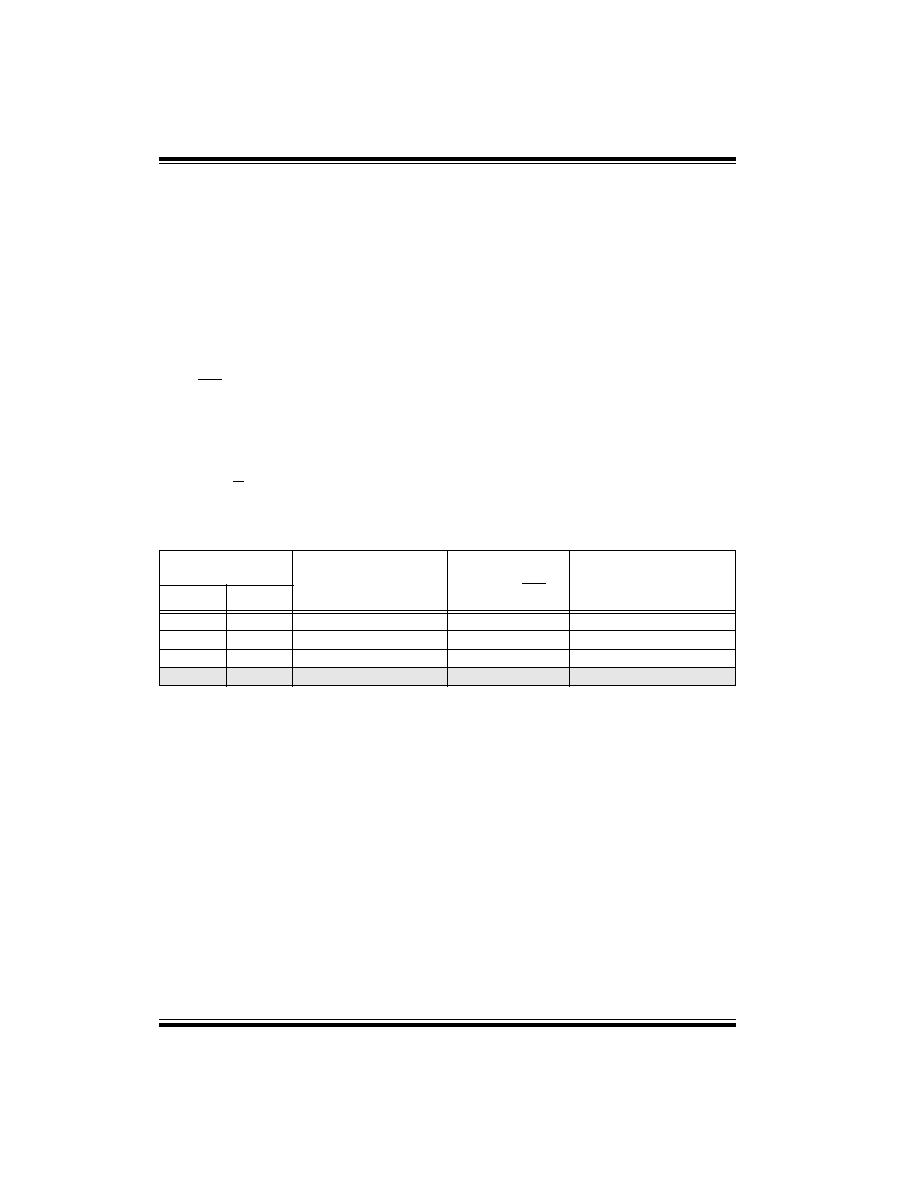
PIC16C72 Series
DS39016A-page 48
Preliminary
©
1998 Microchip Technology Inc.
8.4.1.1
ADDRESSING
Once the SSP module has been enabled, it waits for a
START condition to occur. Following the START condi-
tion, the 8-bits are shifted into the SSPSR register. All
incoming bits are sampled with the rising edge of the
clock (SCL) line. The value of register SSPSR<7:1> is
compared to the value of the SSPADD register. The
address is compared on the falling edge of the eighth
clock (SCL) pulse. If the addresses match, and the BF
and SSPOV bits are clear, the following events occur:
a)
The SSPSR register value is loaded into the
SSPBUF register.
b)
The buffer full bit, BF is set.
c)
An ACK pulse is generated.
d)
SSP interrupt flag bit, SSPIF (PIR1<3>) is set
(interrupt is generated if enabled) - on the falling
edge of the ninth SCL pulse.
In 10-bit address mode, two address bytes need to be
received by the slave. The five Most Significant bits
(MSbs) of the first address byte specify if this is a 10-bit
address. Bit R/W (SSPSTAT<2>) must specify a write
so the slave device will receive the second address
byte. For a 10-bit address the first byte would equal
`
1111 0 A9 A8 0
', where A9 and A8 are the two MSbs
of the address. The sequence of events for 10-bit
address is as follows, with steps 7- 9 for slave-transmit-
ter:
1.
Receive first (high) byte of Address (bits SSPIF,
BF, and bit UA (SSPSTAT<1>) are set).
2.
Update the SSPADD register with second (low)
byte of Address (clears bit UA and releases the
SCL line).
3.
Read the SSPBUF register (clears bit BF) and
clear flag bit SSPIF.
4.
Receive second (low) byte of Address (bits
SSPIF, BF, and UA are set).
5.
Update the SSPADD register with the first (high)
byte of Address, if match releases SCL line, this
will clear bit UA.
6.
Read the SSPBUF register (clears bit BF) and
clear flag bit SSPIF.
7.
Receive repeated START condition.
8.
Receive first (high) byte of Address (bits SSPIF
and BF are set).
9.
Read the SSPBUF register (clears bit BF) and
clear flag bit SSPIF.
TABLE 8-3
DATA TRANSFER RECEIVED BYTE ACTIONS
Status Bits as Data
Transfer is Received
SSPSR
SSPBUF
Generate ACK
Pulse
Set bit SSPIF
(SSP Interrupt occurs
if enabled)
BF
SSPOV
0
0
Yes
Yes
Yes
1
0
No
No
Yes
1
1
No
No
Yes
0
1
No
No
Yes
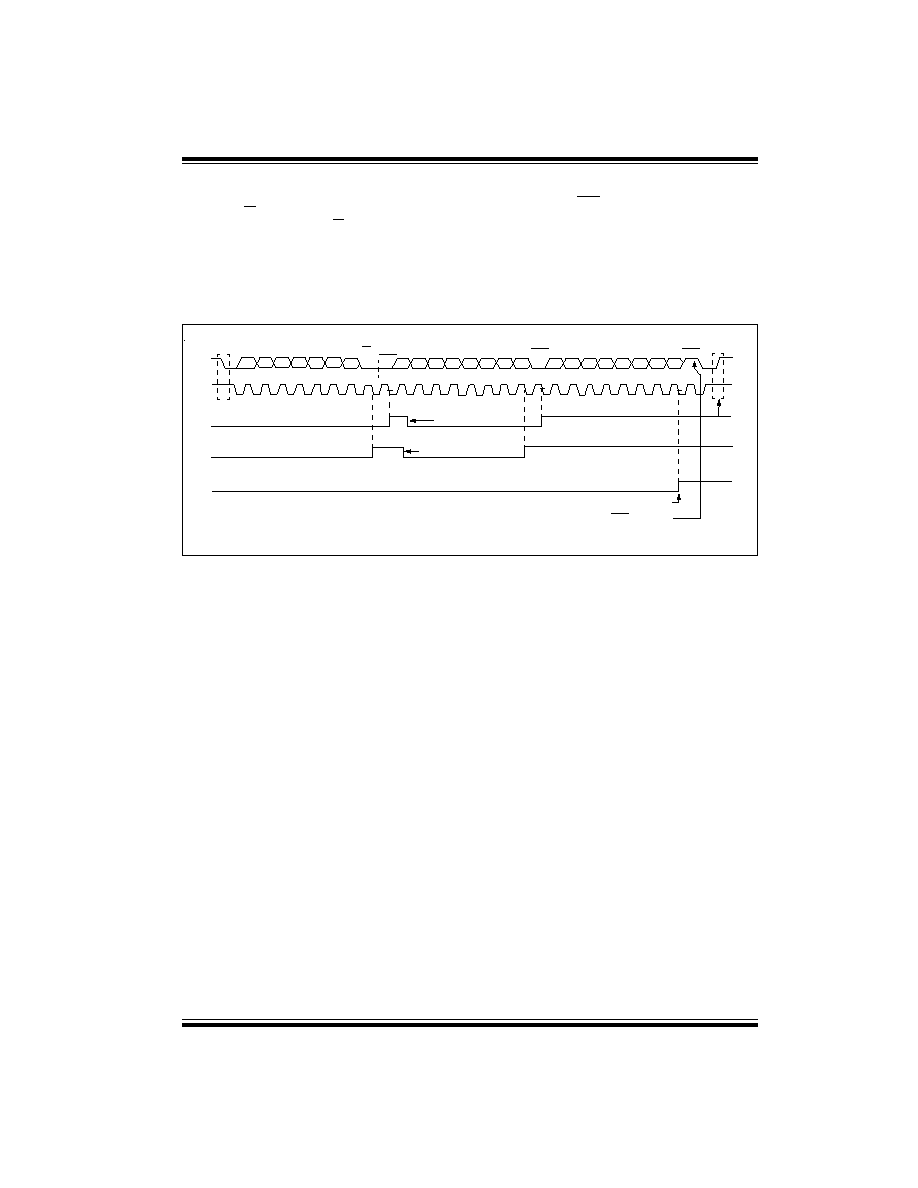
PIC16C72 Series
©
1998 Microchip Technology Inc.
Preliminary
DS39016A-page 49
8.4.1.2
RECEPTION
When the R/W bit of the address byte is clear and an
address match occurs, the R/W bit of the SSPSTAT
register is cleared. The received address is loaded into
the SSPBUF register.
When the address byte overflow condition exists, then
no acknowledge (ACK) pulse is given. An overflow con-
dition is defined as either bit BF (SSPSTAT<0>) is set
or bit SSPOV (SSPCON<6>) is set.
An SSP interrupt is generated for each data transfer
byte. Flag bit SSPIF (PIR1<3>) must be cleared in soft-
ware. The SSPSTAT register is used to determine the
status of the byte.
FIGURE 8-8:
I
2
C WAVEFORMS FOR RECEPTION (7-BIT ADDRESS)
P
9
8
7
6
5
D0
D1
D2
D3
D4
D5
D6
D7
S
A7 A6 A5 A4 A3 A2 A1
SDA
SCL
1
2
3
4
5
6
7
8
9
1
2
3
4
5
6
7
8
9
1
2
3
4
Bus Master
terminates
transfer
Bit SSPOV is set because the SSPBUF register is still full.
Cleared in software
SSPBUF register is read
ACK
Receiving Data
Receiving Data
D0
D1
D2
D3
D4
D5
D6
D7
ACK
R/W=0
Receiving Address
SSPIF (PIR1<3>)
BF (SSPSTAT<0>)
SSPOV (SSPCON<6>)
ACK
ACK is not sent.
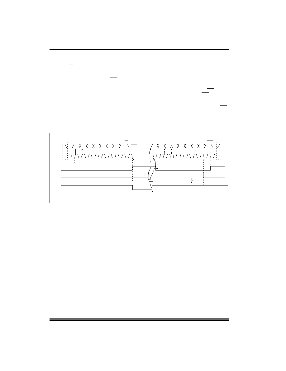
PIC16C72 Series
DS39016A-page 50
Preliminary
©
1998 Microchip Technology Inc.
8.4.1.3
TRANSMISSION
When the R/W bit of the incoming address byte is set
and an address match occurs, the R/W bit of the
SSPSTAT register is set. The received address is
loaded into the SSPBUF register. The ACK pulse will
be sent on the ninth bit, and pin RC3/SCK/SCL is held
low. The transmit data must be loaded into the SSP-
BUF register, which also loads the SSPSR register.
Then pin RC3/SCK/SCL should be enabled by setting
bit CKP (SSPCON<4>). The master must monitor the
SCL pin prior to asserting another clock pulse. The
slave devices may be holding off the master by stretch-
ing the clock. The eight data bits are shifted out on the
falling edge of the SCL input. This ensures that the SDA
signal is valid during the SCL high time (Figure 8-9).
An SSP interrupt is generated for each data transfer
byte. Flag bit SSPIF must be cleared in software, and
the SSPSTAT register is used to determine the status
of the byte. Flag bit SSPIF is set on the falling edge of
the ninth clock pulse.
As a slave-transmitter, the ACK pulse from the master-
receiver is latched on the rising edge of the ninth SCL
input pulse. If the SDA line was high (not ACK), then the
data transfer is complete. When the ACK is latched by
the slave, the slave logic is reset (resets SSPSTAT reg-
ister) and the slave then monitors for another occur-
rence of the START bit. If the SDA line was low (ACK),
the transmit data must be loaded into the SSPBUF reg-
ister, which also loads the SSPSR register. Then pin
RC3/SCK/SCL should be enabled by setting bit CKP.
FIGURE 8-9:
I
2
C WAVEFORMS FOR TRANSMISSION (7-BIT ADDRESS)
SDA
SCL
SSPIF (PIR1<3>)
BF (SSPSTAT<0>)
CKP (SSPCON<4>)
A7
A6
A5
A4
A3
A2
A1
ACK
D7
D6
D5
D4
D3
D2
D1
D0
ACK
Transmitting Data
R/W = 1
Receiving Address
1
2
3
4
5
6
7
8
9
1
2
3
4
5
6
7
8
9
P
cleared in software
SSPBUF is written in software
From SSP interrupt
service routine
Set bit after writing to SSPBUF
S
Data in
sampled
SCL held low
while CPU
responds to SSPIF
(the SSPBUF must be written-to
before the CKP bit can be set)
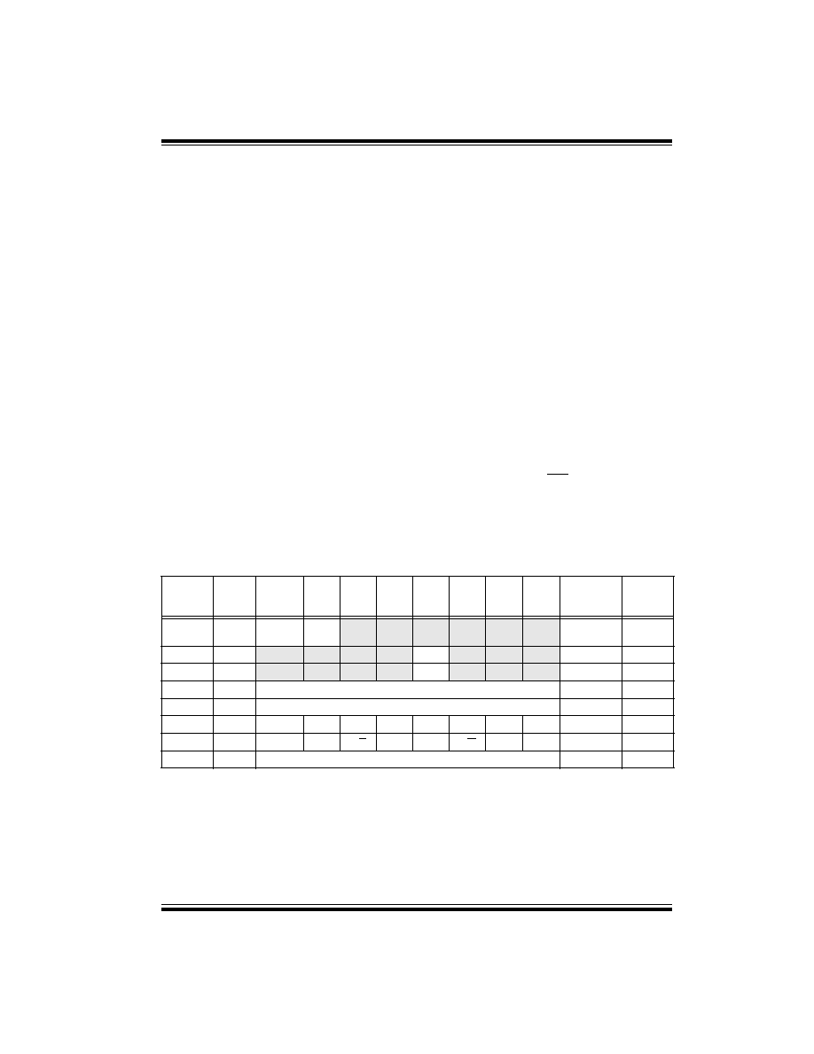
PIC16C72 Series
©
1998 Microchip Technology Inc.
Preliminary
DS39016A-page 51
8.4.2
MASTER OPERATION
Master operation is supported in firmware using inter-
rupt generation on the detection of the START and
STOP conditions. The STOP (P) and START (S) bits
are cleared from a reset or when the SSP module is
disabled. The STOP (P) and START (S) bits will toggle
based on the START and STOP conditions. Control of
the I
2
C bus may be taken when the P bit is set, or the
bus is idle and both the S and P bits are clear.
In master operation, the SCL and SDA lines are manip-
ulated in firmware by clearing the corresponding
TRISC<4:3> bit(s). The output level is always low, irre-
spective of the value(s) in PORTC<4:3>. So when
transmitting data, a '1' data bit must have the
TRISC<4> bit set (input) and a '0' data bit must have
the TRISC<4> bit cleared (output). The same scenario
is true for the SCL line with the TRISC<3> bit.
The following events will cause SSP Interrupt Flag bit,
SSPIF, to be set (SSP Interrupt if enabled):
∑ START condition
∑ STOP condition
∑ Data transfer byte transmitted/received
Master operation can be done with either the slave
mode idle (SSPM3:SSPM0 =
1011
) or with the slave
active. When both master operation and slave modes
are used, the software needs to differentiate the
source(s) of the interrupt.
For more information on master operation, see
AN554
- Software Implementation of I
2
C Bus Master.
8.4.3
MULTI-MASTER OPERATION
In multi-master operation, the interrupt generation on
the detection of the START and STOP conditions
allows the determination of when the bus is free. The
STOP (P) and START (S) bits are cleared from a reset
or when the SSP module is disabled. The STOP (P)
and START (S) bits will toggle based on the START and
STOP conditions. Control of the I
2
C bus may be taken
when bit P (SSPSTAT<4>) is set, or the bus is idle and
both the S and P bits clear. When the bus is busy,
enabling the SSP Interrupt will generate the interrupt
when the STOP condition occurs.
In multi-master operation, the SDA line must be moni-
tored to see if the signal level is the expected output
level. This check only needs to be done when a high
level is output. If a high level is expected and a low level
is present, the device needs to release the SDA and
SCL lines (set TRISC<4:3>). There are two stages
where this arbitration can be lost, these are:
∑ Address Transfer
∑ Data Transfer
When the slave logic is enabled, the slave continues to
receive. If arbitration was lost during the address trans-
fer stage, communication to the device may be in
progress. If addressed an ACK pulse will be generated.
If arbitration was lost during the data transfer stage, the
device will need to re-transfer the data at a later time.
For more information on master operation, see
AN578
- Use of the SSP Module in the of I
2
C Multi-Master
Environment.
TABLE 8-4
REGISTERS ASSOCIATED WITH I
2
C OPERATION
Address
Name
Bit 7
Bit 6
Bit 5
Bit 4
Bit 3
Bit 2
Bit 1
Bit 0
Value on
POR,
BOR
Value on
all other
resets
0Bh, 8Bh,
10Bh,18Bh
INTCON
GIE
PEIE
T0IE
INTE
RBIE
T0IF
INTF
RBIF
0000 000x
0000 000u
0Ch
PIR1
(1)
ADIF
(1)
(1)
SSPIF
CCP1IF TMR2IF TMR1IF
0000 0000
0000 0000
8Ch
PIE1
(1)
ADIE
(1)
(1)
SSPIE CCP1IE TMR2IE TMR1IE
0000 0000
0000 0000
13h
SSPBUF Synchronous Serial Port Receive Buffer/Transmit Register
xxxx xxxx
uuuu uuuu
93h
SSPADD Synchronous Serial Port (I
2
C mode) Address Register
0000 0000
0000 0000
14h
SSPCON
WCOL
SSPOV SSPEN
CKP
SSPM3 SSPM2 SSPM1 SSPM0
0000 0000
0000 0000
94h
SSPSTAT
SMP
(2)
CKE
(2)
D/A
P
S
R/W
UA
BF
0000 0000
0000 0000
87h
TRISC
PORTC Data Direction register
1111 1111
1111 1111
Legend:
x
= unknown,
u
= unchanged,
-
= unimplemented locations read as '0'.
Shaded cells are not used by SSP module in SPI mode.
Note 1:
These bits are unimplemented, read as '0'.
2:
The SMP and CKE bits are implemented on the PIC16CR72 only. On the PIC16C72, these two bits are unimplemented,
read as '0'.

PIC16C72 Series
DS39016A-page 52
Preliminary
©
1998 Microchip Technology Inc.
NOTES:

PIC16C72 Series
©
1998 Microchip Technology Inc.
Preliminary
DS39016A-page 53
9.0
ANALOG-TO-DIGITAL
CONVERTER (A/D) MODULE
The analog-to-digital (A/D) converter module has five
inputs for the PIC16C72/R72.
The A/D allows conversion of an analog input signal to
a corresponding 8-bit digital number (refer to Applica-
tion Note AN546 for use of A/D Converter). The output
of the sample and hold is the input into the converter,
which generates the result via successive approxima-
tion. The analog reference voltage is software select-
able to either the device's positive supply voltage (V
DD
)
or the voltage level on the RA3/AN3/V
REF
pin.
The A/D converter has a unique feature of being able
to operate while the device is in SLEEP mode. To oper-
ate in sleep, the A/D conversion clock must be derived
from the A/D's internal RC oscillator.
Additional information on the A/D module is available in
the PICmicroTM Mid-Range MCU Reference Manual,
DS33023.
The A/D module has three registers. These registers
are:
∑ A/D Result Register (ADRES)
∑ A/D Control Register 0 (ADCON0)
∑ A/D Control Register 1 (ADCON1)
A device reset forces all registers to their reset state.
This forces the A/D module to be turned off, and any
conversion is aborted.
The ADCON0 register, shown in Figure 9-1, controls
the operation of the A/D module. The ADCON1 regis-
ter, shown in Figure 9-2, configures the functions of the
port pins. The port pins can be configured as analog
inputs (RA3 can also be a voltage reference) or as dig-
ital I/O.
FIGURE 9-1:
ADCON0 REGISTER (ADDRESS 1Fh)
R/W-0
R/W-0
R/W-0
R/W-0
R/W-0
R/W-0
U-0
R/W-0
ADCS1 ADCS0
CHS2
CHS1
CHS0
GO/DONE
--
ADON
R = Readable bit
W = Writable bit
U = Unimplemented bit,
read as `0'
- n = Value at POR reset
bit7
bit0
bit 7-6:
ADCS1:ADCS0: A/D Conversion Clock Select bits
00
= F
OSC
/2
01
= F
OSC
/8
10
= F
OSC
/32
11
= F
RC
(clock derived from an internal RC oscillator)
bit 5-3: CHS2:CHS0: Analog Channel Select bits
000
= channel 0, (RA0/AN0)
001
= channel 1, (RA1/AN1)
010
= channel 2, (RA2/AN2)
011
= channel 3, (RA3/AN3)
100
= channel 4, (RA5/AN4)
bit 2:
GO/DONE: A/D Conversion Status bit
If ADON = 1
1 = A/D conversion in progress (setting this bit starts the A/D conversion)
0 = A/D conversion not in progress (This bit is automatically cleared by hardware when the A/D conver-
sion is complete)
bit 1:
Unimplemented: Read as '0'
bit 0:
ADON: A/D On bit
1 = A/D converter module is operating
0 = A/D converter module is shutoff and consumes no operating current
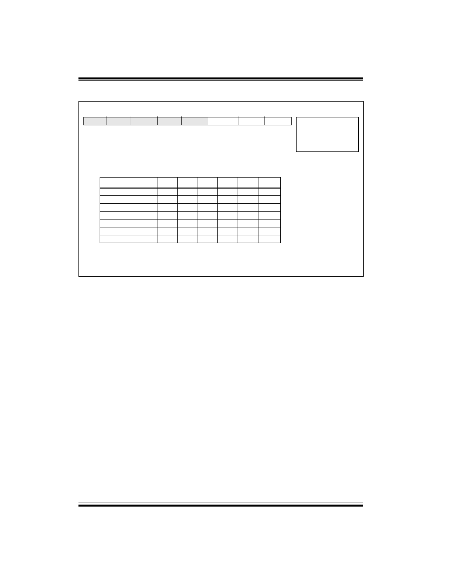
PIC16C72 Series
DS39016A-page 54
Preliminary
©
1998 Microchip Technology Inc.
FIGURE 9-2:
ADCON1 REGISTER (ADDRESS 9Fh)
U-0
U-0
U-0
U-0
U-0
R/W-0
R/W-0
R/W-0
--
--
--
--
--
PCFG2
PCFG1
PCFG0
R = Readable bit
W = Writable bit
U = Unimplemented
bit, read as `0'
- n = Value at POR reset
bit7
bit0
bit 7-3:
Unimplemented: Read as '0'
bit 2-0:
PCFG2:PCFG0: A/D Port Configuration Control bits
A = Analog input
D = Digital I/O
PCFG2:PCFG0
RA0
RA1
RA2
RA5
RA3
V
REF
000
A
A
A
A
A
V
DD
001
A
A
A
A
V
REF
RA3
010
A
A
A
A
A
V
DD
011
A
A
A
A
V
REF
RA3
100
A
A
D
D
A
V
DD
101
A
A
D
D
V
REF
RA3
11x
D
D
D
D
D
GND
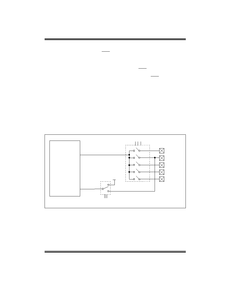
PIC16C72 Series
©
1998 Microchip Technology Inc.
Preliminary
DS39016A-page 55
The ADRES register contains the result of the A/D con-
version. When the A/D conversion is complete, the
result is loaded into the ADRES register, the GO/DONE
bit (ADCON0<2>) is cleared, and A/D interrupt flag bit
ADIF is set. The block diagram of the A/D module is
shown in Figure 9-3.
The value that is in the ADRES register is not modified
for a Power-on Reset. The ADRES register will contain
unknown data after a Power-on Reset.
After the A/D module has been configured as desired,
the selected channel must be acquired before the con-
version is started. The analog input channels must
have their corresponding TRIS bits selected as an
input. To determine acquisition time, see Section 9.1.
After this acquisition time has elapsed the A/D conver-
sion can be started. The following steps should be fol-
lowed for doing an A/D conversion:
1.
Configure the A/D module:
∑ Configure analog pins / voltage reference /
and digital I/O (ADCON1)
∑ Select A/D input channel (ADCON0)
∑ Select A/D conversion clock (ADCON0)
∑ Turn on A/D module (ADCON0)
2.
Configure A/D interrupt (if desired):
∑ Clear ADIF bit
∑ Set ADIE bit
∑ Set GIE bit
3.
Wait the required acquisition time.
4.
Start conversion:
∑ Set GO/DONE bit (ADCON0)
5.
Wait for A/D conversion to complete, by either:
∑ Polling for the GO/DONE bit to be cleared
OR
∑ Waiting for the A/D interrupt
6.
Read A/D Result register (ADRES), clear bit
ADIF if required.
7.
For next conversion, go to step 1 or step 2 as
required. The A/D conversion time per bit is
defined as T
AD
. A minimum wait of 2T
AD
is
required before next acquisition starts.
FIGURE 9-3:
A/D BLOCK DIAGRAM
(Input voltage)
V
AIN
V
REF
(Reference
voltage)
V
DD
PCFG2:PCFG0
CHS2:CHS0
000
or
010
or
100
001
or
011
or
101
RA5/AN4
RA3/AN3/V
REF
RA2/AN2
RA1/AN1
RA0/AN0
100
011
010
001
000
A/D
Converter
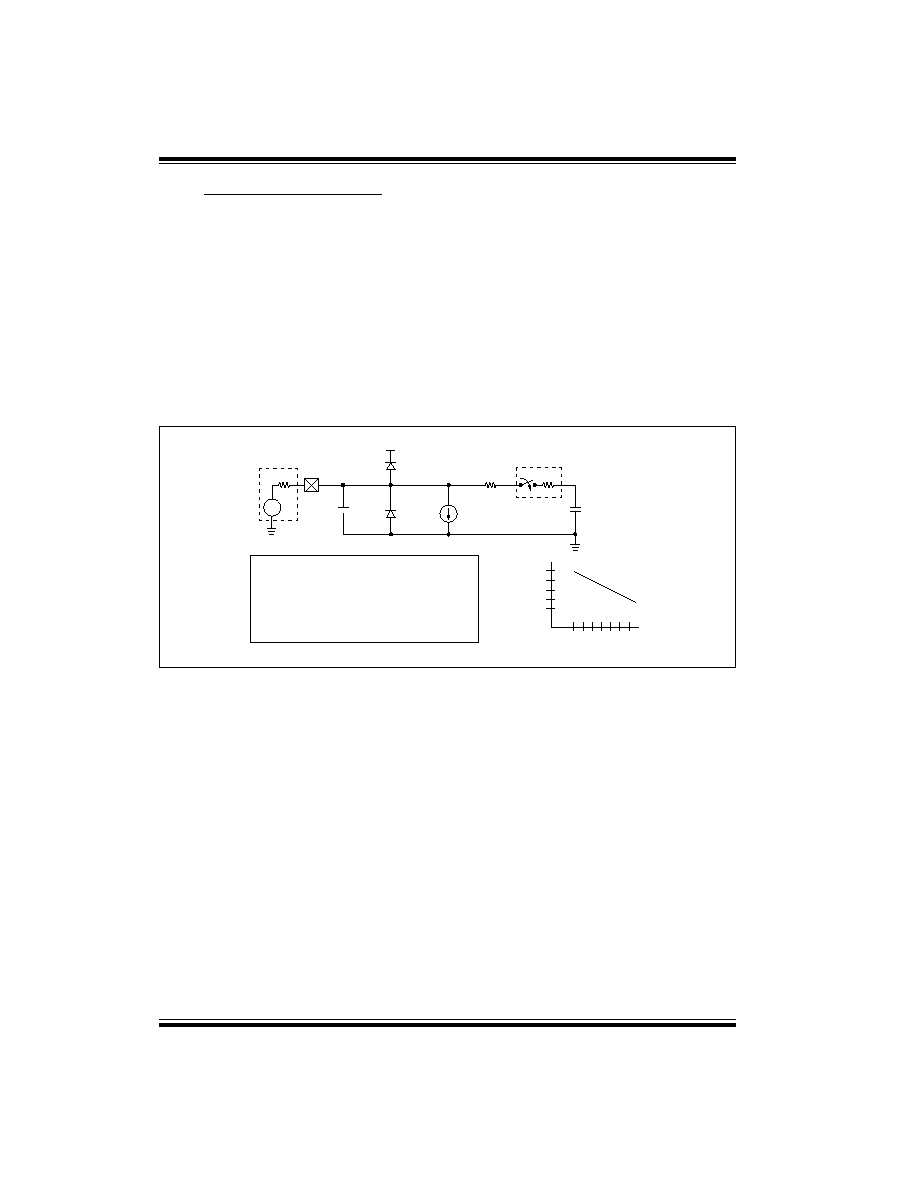
PIC16C72 Series
DS39016A-page 56
Preliminary
©
1998 Microchip Technology Inc.
9.1
A/D Acquisition Requirements
For the A/D converter to meet its specified accuracy,
the charge holding capacitor (C
HOLD
) must be allowed
to fully charge to the input channel voltage level. The
analog input model is shown in Figure 9-4. The source
impedance (R
S
) and the internal sampling switch (R
SS
)
impedance directly affect the time required to charge
the capacitor C
HOLD
. The sampling switch (R
SS
)
impedance varies over the device voltage (V
DD
). The
source impedance affects the offset voltage at the ana-
log input (due to pin leakage current). The maximum
recommended impedance for analog sources is 10
k
. After the analog input channel is selected
(changed) this acquisition must be done before the
conversion can be started.
To calculate the minimum acquisition time, T
ACQ
, see
the PICmicroTM Mid-Range MCU Reference Manual,
DS33023. This equation calculates the acquisition time
to within 1/2 LSb error (512 steps for the A/D). The 1/2
LSb error is the maximum error allowed for the A/D to
meet its specified accuracy.
FIGURE 9-4:
ANALOG INPUT MODEL
C
PIN
VA
Rs
ANx
5 pF
V
DD
V
T
= 0.6V
V
T
= 0.6V
I leakage
R
IC
1k
Sampling
Switch
SS
R
SS
C
HOLD
= DAC capacitance
V
SS
6V
Sampling Switch
5V
4V
3V
2V
5 6 7 8 9 10 11
( k
)
V
DD
= 51.2 pF
±
500 nA
Legend C
PIN
V
T
I leakage
R
IC
SS
C
HOLD
= input capacitance
= threshold voltage
= leakage current at the pin due to
= interconnect resistance
= sampling switch
= sample/hold capacitance (from DAC)
various junctions
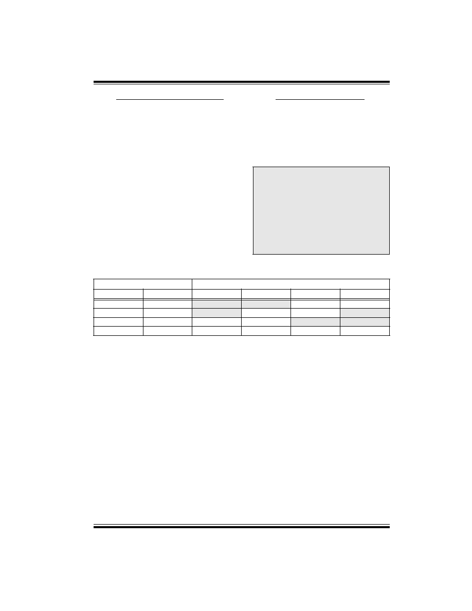
PIC16C72 Series
©
1998 Microchip Technology Inc.
Preliminary
DS39016A-page 57
9.2
Selecting the A/D Conversion Clock
The A/D conversion time per bit is defined as T
AD
. The
A/D conversion requires 9.5T
AD
per 8-bit conversion.
The source of the A/D conversion clock is software
selectable. The four possible options for T
AD
are:
∑ 2T
OSC
∑ 8T
OSC
∑ 32T
OSC
∑ Internal RC oscillator
For correct A/D conversions, the A/D conversion clock
(T
AD
) must be selected to ensure a minimum T
AD
time
of 1.6
µ
s.
Table 9-1 shows the resultant T
AD
times derived from
the device operating frequencies and the A/D clock
source selected.
9.3
Configuring Analog Port Pins
The ADCON1, TRISA, and TRISE registers control the
operation of the A/D port pins. The port pins that are
desired as analog inputs must have their correspond-
ing TRIS bits set (input). If the TRIS bit is cleared (out-
put), the digital output level (V
OH
or V
OL
) will be
converted.
The A/D operation is independent of the state of the
CHS2:CHS0 bits and the TRIS bits.
TABLE 9-1
T
AD
vs. DEVICE OPERATING FREQUENCIES
Note 1: When reading the port register, all pins
configured as analog input channels will
read as cleared (a low level). Pins config-
ured as digital inputs, will convert an ana-
log input. Analog levels on a digitally
configured input will not affect the conver-
sion accuracy.
Note 2: Analog levels on any pin that is defined as
a digital input (including the AN4:AN0
pins), may cause the input buffer to con-
sume current that is out of the devices
specification.
AD Clock Source (T
AD
)
Device Frequency
Operation
ADCS1:ADCS0
20 MHz
5 MHz
1.25 MHz
333.33 kHz
2T
OSC
00
100 ns
(2)
400 ns
(2)
1.6
µ
s
6
µ
s
8T
OSC
01
400 ns
(2)
1.6
µ
s
6.4
µ
s
24
µ
s
(3)
32T
OSC
10
1.6
µ
s
6.4
µ
s
25.6
µ
s
(3)
96
µ
s
(3)
RC
(5)
11
2 - 6
µ
s
(1,4)
2 - 6
µ
s
(1,4)
2 - 6
µ
s
(1,4)
2 - 6
µ
s
(1)
Legend: Shaded cells are outside of recommended range.
Note 1: The RC source has a typical T
AD
time of 4
µ
s.
2: These values violate the minimum required T
AD
time.
3: For faster conversion times, the selection of another clock source is recommended.
4: When device frequency is greater than 1 MHz, the RC A/D conversion clock source is recommended for
sleep operation only.
5: For extended voltage devices (LC), please refer to Electrical Specifications section.
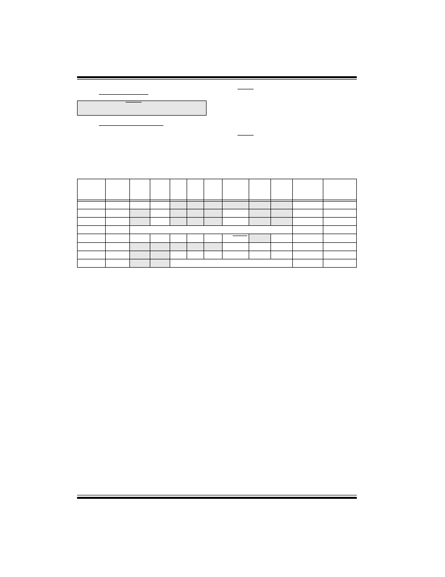
PIC16C72 Series
DS39016A-page 58
Preliminary
©
1998 Microchip Technology Inc.
9.4
A/D Conversions
9.5
Use of the CCP Trigger
An A/D conversion can be started by the "special event
trigger" of the CCP1 module. This requires that the
CCP1M3:CCP1M0 bits (CCP1CON<3:0>) be pro-
grammed as
1011
and that the A/D module is enabled
(ADON bit is set). When the trigger occurs, the
GO/DONE bit will be set, starting the A/D conversion,
and the Timer1 counter will be reset to zero. Timer1 is
reset to automatically repeat the A/D acquisition period
with minimal software overhead (moving the ADRES to
the desired location). The appropriate analog input
channel must be selected and the minimum acquisition
done before the "special event trigger" sets the
GO/DONE bit (starts a conversion).
If the A/D module is not enabled (ADON is cleared),
then the "special event trigger" will be ignored by the
A/D module, but will still reset the Timer1 counter.
TABLE 9-2
REGISTERS/BITS ASSOCIATED WITH A/D
Note:
The GO/DONE bit should NOT be set in
the same instruction that turns on the A/D.
Address
Name
Bit 7
Bit 6
Bit 5
Bit 4
Bit 3
Bit 2
Bit 1
Bit 0
Value on:
POR,
BOR
Value on all
other Resets
0Bh,8Bh
INTCON
GIE
PEIE
T0IE
INTE
RBIE
T0IF
INTF
RBIF
0000 000x
0000 000u
0Ch
PIR1
--
ADIF
--
--
SSPIF
CCP1IF
TMR2IF
TMR1IF
-0-- 0000
-0-- 0000
8Ch
PIE1
--
ADIE
--
--
SSPIE
CCP1IE
TMR2IE TMR1IE
-0-- 0000
-0-- 0000
1Eh
ADRES
A/D Result Register
xxxx xxxx
uuuu uuuu
1Fh
ADCON0
ADCS1 ADCS0 CHS2 CHS1
CHS0
GO/DONE
--
ADON
0000 00-0
0000 00-0
9Fh
ADCON1
--
--
--
--
--
PCFG2
PCFG1
PCFG0
---- -000
---- -000
05h
PORTA
--
--
RA5
RA4
RA3
RA2
RA1
RA0
--0x 0000
--0u 0000
85h
TRISA
--
--
PORTA Data Direction Register
--11 1111
--11 1111
Legend:
x
= unknown,
u
= unchanged,
-
= unimplemented read as '0'. Shaded cells are not used for A/D conversion.

PIC16C72 Series
©
1998 Microchip Technology Inc.
Preliminary
DS39016A-page 59
10.0
SPECIAL FEATURES OF THE
CPU
The PIC16C72 series has a host of such features
intended to maximize system reliability, minimize cost
through elimination of external components, provide
power saving operating modes and offer code protec-
tion. These are:
∑ Oscillator selection
∑ Reset
- Power-on Reset (POR)
- Power-up Timer (PWRT)
- Oscillator Start-up Timer (OST)
- Brown-out Reset (BOR)
∑ Interrupts
∑ Watchdog Timer (WDT)
∑ SLEEP
∑ Code protection
∑ ID locations
∑ In-Circuit Serial ProgrammingTM
The PIC16CXXX family has a Watchdog Timer which
can be shut off only through configuration bits. It runs
off its own RC oscillator for added reliability. There are
two timers that offer necessary delays on power-up.
One is the Oscillator Start-up Timer (OST), intended to
keep the chip in reset until the crystal oscillator is sta-
ble. The other is the Power-up Timer (PWRT), which
provides a fixed delay of 72 ms (nominal) on power-up
only, designed to keep the part in reset while the power
supply stabilizes. With these two timers on-chip, most
applications need no external reset circuitry.
SLEEP mode is designed to offer a very low current
power-down mode. The user can wake-up from SLEEP
through external reset, Watchdog Timer Wake-up, or
through an interrupt. Several oscillator options are also
made available to allow the part to fit the application.
The RC oscillator option saves system cost while the
LP crystal option saves power. A set of configuration
bits are used to select various options.
Additional information on special features is available in
the PICmicroTM Mid-Range MCU Family Reference
Manual, DS33023.
10.1
Configuration Bits
The configuration bits can be programmed (read as '0')
or left unprogrammed (read as '1') to select various
device configurations. These bits are mapped in pro-
gram memory location 2007h.
The user will note that address 2007h is beyond the
user program memory space. In fact, it belongs to the
special test/configuration memory space (2000h -
3FFFh), which can be accessed only during program-
ming.
FIGURE 10-1: CONFIGURATION WORD FOR PIC16C72/R72
CP1
CP0
CP1
CP0
CP1
CP0
--
BODEN
CP1
CP0
PWRTE
WDTE
FOSC1
FOSC0
Register:CONFIG
Address2007h
bit13
bit0
bit 13-8
CP1:CP0: Code Protection bits
(2)
5-4:
11
= Code protection off
10
= Upper half of program memory code protected
01
= Upper 3/4th of program memory code protected
00
= All memory is code protected
bit 7:
Unimplemented: Read as '1'
bit 6:
BODEN: Brown-out Reset Enable bit
(1)
1 = BOR enabled
0 = BOR disabled
bit 3:
PWRTE: Power-up Timer Enable bit
(1)
1 = PWRT disabled
0 = PWRT enabled
bit 2:
WDTE: Watchdog Timer Enable bit
1 = WDT enabled
0 = WDT disabled
bit 1-0:
FOSC1:FOSC0: Oscillator Selection bits
11
= RC oscillator
10
= HS oscillator
01
= XT oscillator
00
= LP oscillator
Note 1:
Enabling Brown-out Reset automatically enables Power-up Timer (PWRT) regardless of the value of bit PWRTE.
Ensure the Power-up Timer is enabled anytime Brown-out Reset is enabled.
2: All of the CP1:CP0 pairs have to be given the same value to enable the code protection scheme listed.
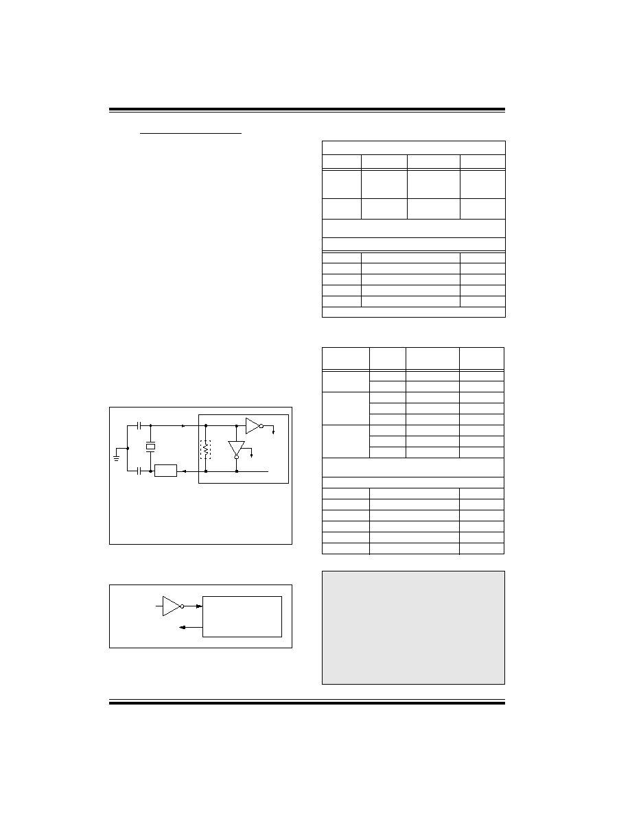
PIC16C72 Series
DS39016A-page 60
Preliminary
©
1998 Microchip Technology Inc.
10.2
Oscillator Configurations
10.2.1
OSCILLATOR TYPES
The PIC16CXXX family can be operated in four differ-
ent oscillator modes. The user can program two config-
uration bits (FOSC1 and FOSC0) to select one of these
four modes:
∑ LP
Low Power Crystal
∑ XT
Crystal/Resonator
∑ HS
High Speed Crystal/Resonator
∑ RC
Resistor/Capacitor
10.2.2
CRYSTAL OSCILLATOR/CERAMIC
RESONATORS
In XT, LP or HS modes a crystal or ceramic resonator
is connected to the OSC1/CLKIN and OSC2/CLKOUT
pins to establish oscillation (Figure
10-2). The
PIC16CXXX family oscillator design requires the use of
a parallel cut crystal. Use of a series cut crystal may
give a frequency out of the crystal manufacturers spec-
ifications. When in XT, LP or HS modes, the device can
have an external clock source to drive the OSC1/
CLKIN pin (Figure 10-3).
FIGURE 10-2: CRYSTAL/CERAMIC
RESONATOR OPERATION
(HS, XT OR LP
OSC CONFIGURATION)
FIGURE 10-3: EXTERNAL CLOCK INPUT
OPERATION (HS, XT OR LP
OSC CONFIGURATION)
TABLE 10-1
CERAMIC RESONATORS
TABLE 10-2
CAPACITOR SELECTION
FOR CRYSTAL OSCILLATOR
Note1:
See Table 10-1 and Table 10-2 for recom-
mended values of C1 and C2.
2:
A series resistor (RS) may be required for
AT strip cut crystals.
3:
RF varies with the crystal chosen.
C1
(1)
C2
(1)
XTAL
OSC2
OSC1
RF
(3)
SLEEP
To
logic
PIC16CXXX
RS
(2)
internal
OSC1
OSC2
Open
Clock from
ext. system
PIC16CXXX
Ranges Tested:
Mode
Freq
OSC1
OSC2
XT
455 kHz
2.0 MHz
4.0 MHz
68 - 100 pF
15 - 68 pF
15 - 68 pF
68 - 100 pF
15 - 68 pF
15 - 68 pF
HS
8.0 MHz
16.0 MHz
10 - 68 pF
10 - 22 pF
10 - 68 pF
10 - 22 pF
These values are for design guidance only. See
notes at bottom of page.
Resonators Used:
455 kHz
Panasonic EFO-A455K04B
±
0.3%
2.0 MHz
Murata Erie CSA2.00MG
±
0.5%
4.0 MHz
Murata Erie CSA4.00MG
±
0.5%
8.0 MHz
Murata Erie CSA8.00MT
±
0.5%
16.0 MHz Murata Erie CSA16.00MX
±
0.5%
All resonators used did not have built-in capacitors.
Osc Type
Crystal
Freq
Cap. Range
C1
Cap. Range
C2
LP
32 kHz
33 pF
33 pF
200 kHz
15 pF
15 pF
XT
200 kHz
47-68 pF
47-68 pF
1 MHz
15 pF
15 pF
4 MHz
15 pF
15 pF
HS
4 MHz
15 pF
15 pF
8 MHz
15-33 pF
15-33 pF
20 MHz
15-33 pF
15-33 pF
These values are for design guidance only. See
notes at bottom of page.
Crystals Used
32 kHz
Epson C-001R32.768K-A
±
20 PPM
200 kHz
STD XTL 200.000KHz
±
20 PPM
1 MHz
ECS ECS-10-13-1
±
50 PPM
4 MHz
ECS ECS-40-20-1
±
50 PPM
8 MHz
EPSON CA-301 8.000M-C
±
30 PPM
20 MHz
EPSON CA-301 20.000M-C
±
30 PPM
Note 1: Recommended values of C1 and C2 are
identical to the ranges tested (Table 10-1).
2: Higher capacitance increases the stability
of oscillator but also increases the start-up
time.
3: Since each resonator/crystal has its own
characteristics, the user should consult the
resonator/crystal manufacturer for appropri-
ate values of external components.
4: Rs may be required in HS mode as well as
XT mode to avoid overdriving crystals with
low drive level specification.
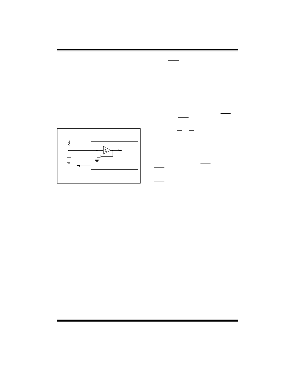
PIC16C72 Series
©
1998 Microchip Technology Inc.
Preliminary
DS39016A-page 61
10.2.3
RC OSCILLATOR
For timing insensitive applications the "RC" device
option offers additional cost savings. The RC oscillator
frequency is a function of the supply voltage, the resis-
tor (R
EXT
) and capacitor (C
EXT
) values, and the operat-
ing temperature. In addition to this, the oscillator
frequency will vary from unit to unit due to normal pro-
cess parameter variation. Furthermore, the difference
in lead frame capacitance between package types will
also affect the oscillation frequency, especially for low
C
EXT
values. The user also needs to take into account
variation due to tolerance of external R and C compo-
nents used. Figure 10-4 shows how the R/C combina-
tion is connected to the PIC16CXXX family.
FIGURE 10-4: RC OSCILLATOR MODE
10.3
Reset
The PIC16CXXX family differentiates between various
kinds of reset:
∑ Power-on Reset (POR)
∑ MCLR reset during normal operation
∑ MCLR reset during SLEEP
∑ WDT Reset (normal operation)
∑ Brown-out Reset (BOR)
Some registers are not affected in any reset condition;
their status is unknown on POR and unchanged in any
other reset. Most other registers are reset to a "reset
state" on Power-on Reset (POR), on the MCLR and
WDT Reset, on MCLR reset during SLEEP, and Brown-
out Reset (BOR). They are not affected by a WDT
Wake-up, which is viewed as the resumption of normal
operation. The TO and PD bits are set or cleared differ-
ently in different reset situations as indicated in
Table
10-4. These bits are used in software to deter-
mine the nature of the reset. See Table 10-6 for a full
description of reset states of all registers.
A simplified block diagram of the on-chip reset circuit is
shown in Figure 10-5.
The PIC16C72/CR72 have a MCLR noise filter in the
MCLR reset path. The filter will detect and ignore small
pulses.
It should be noted that a WDT Reset
does not drive
MCLR pin low.
OSC2/CLKOUT
Cext
Rext
PIC16CXXX
OSC1
Fosc/4
Internal
clock
V
DD
V
SS
Recommended values:
3 k
Rext
100 k
Cext > 20pF
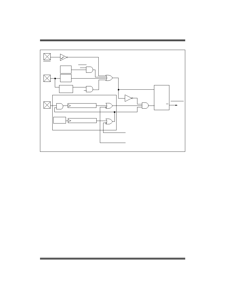
PIC16C72 Series
DS39016A-page 62
Preliminary
©
1998 Microchip Technology Inc.
FIGURE 10-5: SIMPLIFIED BLOCK DIAGRAM OF ON-CHIP RESET CIRCUIT
S
R
Q
External
Reset
MCLR
V
DD
OSC1
WDT
Module
V
DD
rise
detect
OST/PWRT
On-chip
RC OSC
WDT
Time-out
Power-on Reset
OST
10-bit Ripple counter
PWRT
Chip_Reset
10-bit Ripple counter
Reset
Enable OST
Enable PWRT
SLEEP
Note 1:
This is a separate oscillator from the RC oscillator of the CLKIN pin.
Brown-out
Reset
BODEN
(1)
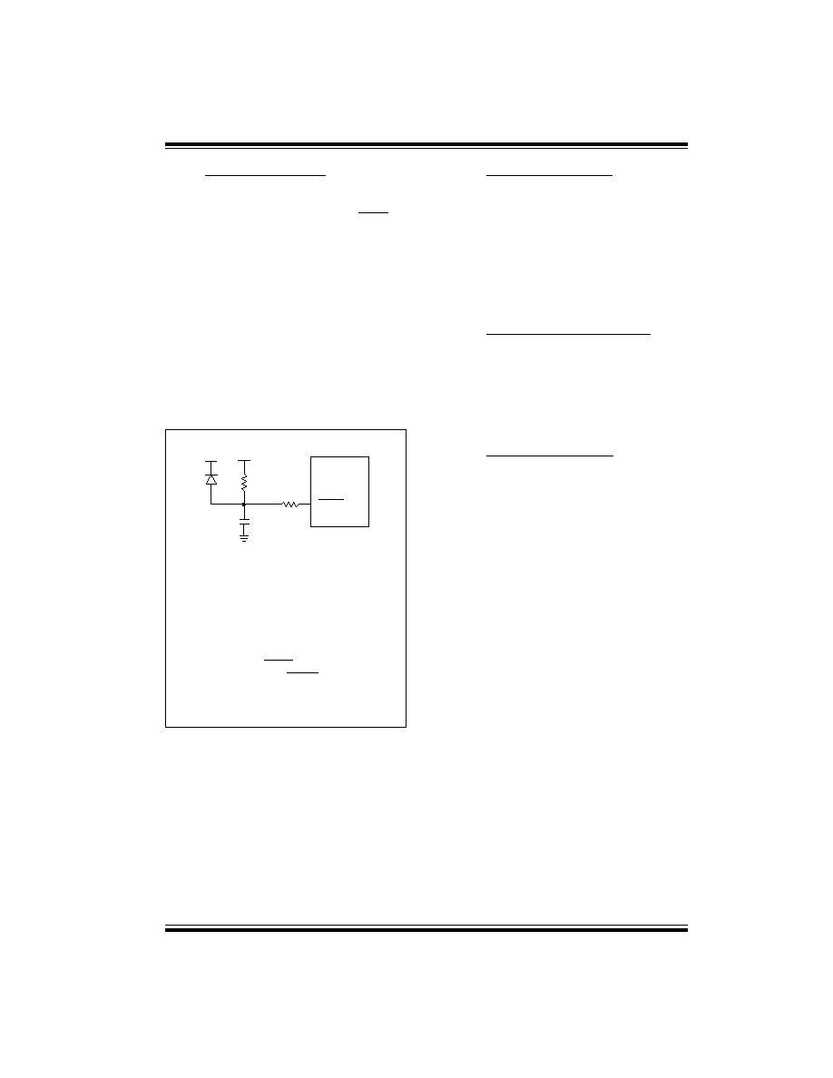
PIC16C72 Series
©
1998 Microchip Technology Inc.
Preliminary
DS39016A-page 63
10.4
Power-On Reset (POR)
A Power-on Reset pulse is generated on-chip when
V
DD
rise is detected (in the range of 1.5V - 2.1V). To
take advantage of the POR, just tie the MCLR pin
directly (or through a resistor) to V
DD
. This will eliminate
external RC components usually needed to create a
Power-on Reset. A maximum rise time for V
DD
is spec-
ified. See Electrical Specifications for details. For a
slow rise time, see Figure 10-6.
When the device starts normal operation (exits the
reset condition), device operating parameters (voltage,
frequency, temperature,...) must be met to ensure oper-
ation. If these conditions are not met, the device must
be held in reset until the operating conditions are met.
Brown-out Reset may be used to meet the startup con-
ditions.
FIGURE 10-6: EXTERNAL POWER-ON
RESET CIRCUIT (FOR SLOW
V
DD
POWER-UP)
10.5
Power-up Timer (PWRT)
The Power-up Timer provides a fixed 72 ms nominal
time-out on power-up only, from the POR. The Power-
up Timer operates on an internal RC oscillator. The
chip is kept in reset as long as the PWRT is active. The
PWRT's time delay allows V
DD
to rise to an acceptable
level. A configuration bit is provided to enable/disable
the PWRT.
The power-up time delay will vary from chip to chip due
to V
DD
, temperature, and process variation. See DC
parameters for details.
10.6
Oscillator Start-up Timer (OST)
The Oscillator Start-up Timer (OST) provides 1024
oscillator cycle (from OSC1 input) delay after the
PWRT delay is over. This ensures that the crystal oscil-
lator or resonator has started and stabilized.
The OST time-out is invoked only for XT, LP and HS
modes and only on Power-on Reset or wake-up from
SLEEP.
10.7
Brown-Out Reset (BOR)
A configuration bit, BODEN, can disable (if clear/pro-
grammed) or enable (if set) the Brown-out Reset cir-
cuitry. If V
DD
falls below 4.0V (3.8V - 4.2V range) for
greater than parameter #35, the brown-out situation will
reset the chip. A reset may not occur if V
DD
falls below
4.0V for less than parameter #35. The chip will remain
in Brown-out Reset until V
DD
rises above BV
DD
. The
Power-up Timer will now be invoked and will keep the
chip in RESET an additional 72 ms. If V
DD
drops below
BV
DD
while the Power-up Timer is running, the chip will
go back into a Brown-out Reset and the Power-up
Timer will be initialized. Once V
DD
rises above BV
DD
,
the Power-up Timer will execute a 72 ms time delay.
The Power-up Timer should always be enabled when
Brown-out Reset is enabled.
Note 1: External Power-on Reset circuit is
required only if V
DD
power-up slope is too
slow. The diode D helps discharge the
capacitor quickly when V
DD
powers down.
2: R < 40 k
is recommended to make sure
that voltage drop across R does not violate
the device's electrical specification.
3: R1 = 100
to 1 k
will limit any current
flowing into MCLR from external capacitor
C in the event of MCLR/V
PP
pin break-
down due to Electrostatic Discharge
(ESD) or Electrical Overstress (EOS).
C
R1
R
D
V
DD
MCLR
PIC16CXXX
PIC16C72 Series
DS39016A-page 64
Preliminary
©
1998 Microchip Technology Inc.
10.8
Time-out Sequence
On power-up the time-out sequence is as follows: First
PWRT time-out is invoked after the POR time delay has
expired. Then OST is activated. The total time-out will
vary based on oscillator configuration and the status of
the PWRT. For example, in RC mode with the PWRT
disabled, there will be no time-out at all. Figure 10-7,
Figure 10-8, Figure 10-9 and Figure 10-10 depict time-
out sequences on power-up.
Since the time-outs occur from the POR pulse, if MCLR
is kept low long enough, the time-outs will expire. Then
bringing MCLR high will begin execution immediately
(Figure 10-9). This is useful for testing purposes or to
synchronize more than one PIC16CXXX family device
operating in parallel.
Table 10-5 shows the reset conditions for some special
function registers, while Table 10-6 shows the reset
conditions for all the registers.
10.9
Power Control/Status Register
(PCON)
The Power Control/Status Register, PCON has up to
two bits, depending upon the device.
Bit0 is Brown-out Reset Status bit, BOR. Bit BOR is
unknown on a Power-on Reset. It must then be set by
the user and checked on subsequent resets to see if bit
BOR cleared, indicating a BOR occurred. The BOR bit
is a "Don't Care" bit and is not necessarily predictable
if the Brown-out Reset circuitry is disabled (by clearing
bit BODEN in the Configuration Word).
Bit1 is POR (Power-on Reset Status bit). It is cleared
on a Power-on Reset and unaffected otherwise. The
user must set this bit following a Power-on Reset.
TABLE 10-3
TIME-OUT IN VARIOUS SITUATIONS
TABLE 10-4
STATUS BITS AND THEIR SIGNIFICANCE
TABLE 10-5
RESET CONDITION FOR SPECIAL REGISTERS
Oscillator Configura-
tion
Power-up
Brown-out
Wake-up from
SLEEP
PWRTE = 0
PWRTE = 1
XT, HS, LP
72 ms +
1024T
OSC
1024T
OSC
72 ms + 1024T
OSC
1024T
OSC
RC
72 ms
--
72 ms
--
POR
BOR
TO
PD
0
x
1
1
Power-on Reset
0
x
0
x
Illegal, TO is set on POR
0
x
x
0
Illegal, PD is set on POR
1
0
x
x
Brown-out Reset
1
1
0
1
WDT Reset
1
1
0
0
WDT Wake-up
1
1
u
u
MCLR Reset during normal operation
1
1
1
0
MCLR Reset during SLEEP or interrupt wake-up from SLEEP
Condition
Program
Counter
STATUS
Register
PCON
Register
Power-on Reset
000h
0001 1xxx
---- --0x
MCLR Reset during normal operation
000h
000u uuuu
---- --uu
MCLR Reset during SLEEP
000h
0001 0uuu
---- --uu
WDT Reset
000h
0000 1uuu
---- --uu
WDT Wake-up
PC + 1
uuu0 0uuu
---- --uu
Brown-out Reset
000h
0001 1uuu
---- --u0
Interrupt wake-up from SLEEP
PC + 1
(1)
uuu1 0uuu
---- --uu
Legend:
u
= unchanged,
x
= unknown,
-
= unimplemented bit read as '0'.
Note 1:
When the wake-up is due to an interrupt and the GIE bit is set, the PC is loaded with the interrupt vector (0004h).
PIC16C72 Series
©
1998 Microchip Technology Inc.
Preliminary
DS39016A-page 65
TABLE 10-6
INITIALIZATION CONDITIONS FOR ALL REGISTERS
Register
Power-on Reset,
Brown-out Reset
MCLR Resets
WDT Reset
Wake-up via WDT or Inter-
rupt
W
xxxx xxxx
uuuu uuuu
uuuu uuuu
INDF
N/A
N/A
N/A
TMR0
xxxx xxxx
uuuu uuuu
uuuu uuuu
PCL
0000h
0000h
PC + 1
(2)
STATUS
0001 1xxx
000q quuu
(3)
uuuq quuu
(3)
FSR
xxxx xxxx
uuuu uuuu
uuuu uuuu
PORTA
--0x 0000
--0u 0000
--uu uuuu
PORTB
xxxx xxxx
uuuu uuuu
uuuu uuuu
PORTC
xxxx xxxx
uuuu uuuu
uuuu uuuu
PCLATH
---0 0000
---0 0000
---u uuuu
INTCON
0000 000x
0000 000u
uuuu uuuu
(1)
PIR1
-0-- 0000
-0-- 0000
-u-- uuuu
(1)
TMR1L
xxxx xxxx
uuuu uuuu
uuuu uuuu
TMR1H
xxxx xxxx
uuuu uuuu
uuuu uuuu
T1CON
--00 0000
--uu uuuu
--uu uuuu
TMR2
0000 0000
0000 0000
uuuu uuuu
T2CON
-000 0000
-000 0000
-uuu uuuu
SSPBUF
xxxx xxxx
uuuu uuuu
uuuu uuuu
SSPCON
0000 0000
0000 0000
uuuu uuuu
CCPR1L
xxxx xxxx
uuuu uuuu
uuuu uuuu
CCPR1H
xxxx xxxx
uuuu uuuu
uuuu uuuu
CCP1CON
--00 0000
--00 0000
--uu uuuu
ADRES
xxxx xxxx
uuuu uuuu
uuuu uuuu
ADCON0
0000 00-0
0000 00-0
uuuu uu-u
OPTION
1111 1111
1111 1111
uuuu uuuu
TRISA
--11 1111
--11 1111
--uu uuuu
TRISB
1111 1111
1111 1111
uuuu uuuu
TRISC
1111 1111
1111 1111
uuuu uuuu
PIE1
-0-- 0000
-0-- 0000
-u-- uuuu
PCON
---- --0u
---- --uu
---- --uu
PR2
1111 1111
1111 1111
1111 1111
SSPADD
0000 0000
0000 0000
uuuu uuuu
SSPSTAT
--00 0000
--00 0000
--uu uuuu
ADCON1
---- -000
---- -000
---- -uuu
Legend:
u
= unchanged,
x
= unknown,
-
= unimplemented bit, read as '0',
q
= value depends on condition
Note 1: One or more bits in INTCON, PIR1 and/or PIR2 will be affected (to cause wake-up).
2: When the wake-up is due to an interrupt and the GIE bit is set, the PC is loaded with the interrupt vector
(0004h).
3: See Table 10-5 for reset value for specific condition.
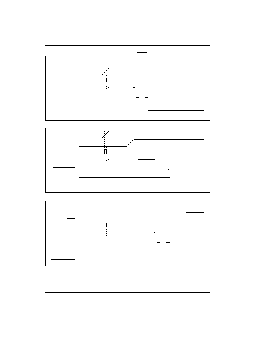
PIC16C72 Series
DS39016A-page 66
Preliminary
©
1998 Microchip Technology Inc.
FIGURE 10-7: TIME-OUT SEQUENCE ON POWER-UP (MCLR TIED TO V
DD
)
FIGURE 10-8: TIME-OUT SEQUENCE ON POWER-UP (MCLR NOT TIED TO V
DD
): CASE 1
FIGURE 10-9: TIME-OUT SEQUENCE ON POWER-UP (MCLR NOT TIED TO V
DD
): CASE 2
T
PWRT
T
OST
V
DD
MCLR
INTERNAL POR
PWRT TIME-OUT
OST TIME-OUT
INTERNAL RESET
T
PWRT
T
OST
V
DD
MCLR
INTERNAL POR
PWRT TIME-OUT
OST TIME-OUT
INTERNAL RESET
V
DD
MCLR
INTERNAL POR
PWRT TIME-OUT
OST TIME-OUT
INTERNAL RESET
T
PWRT
T
OST
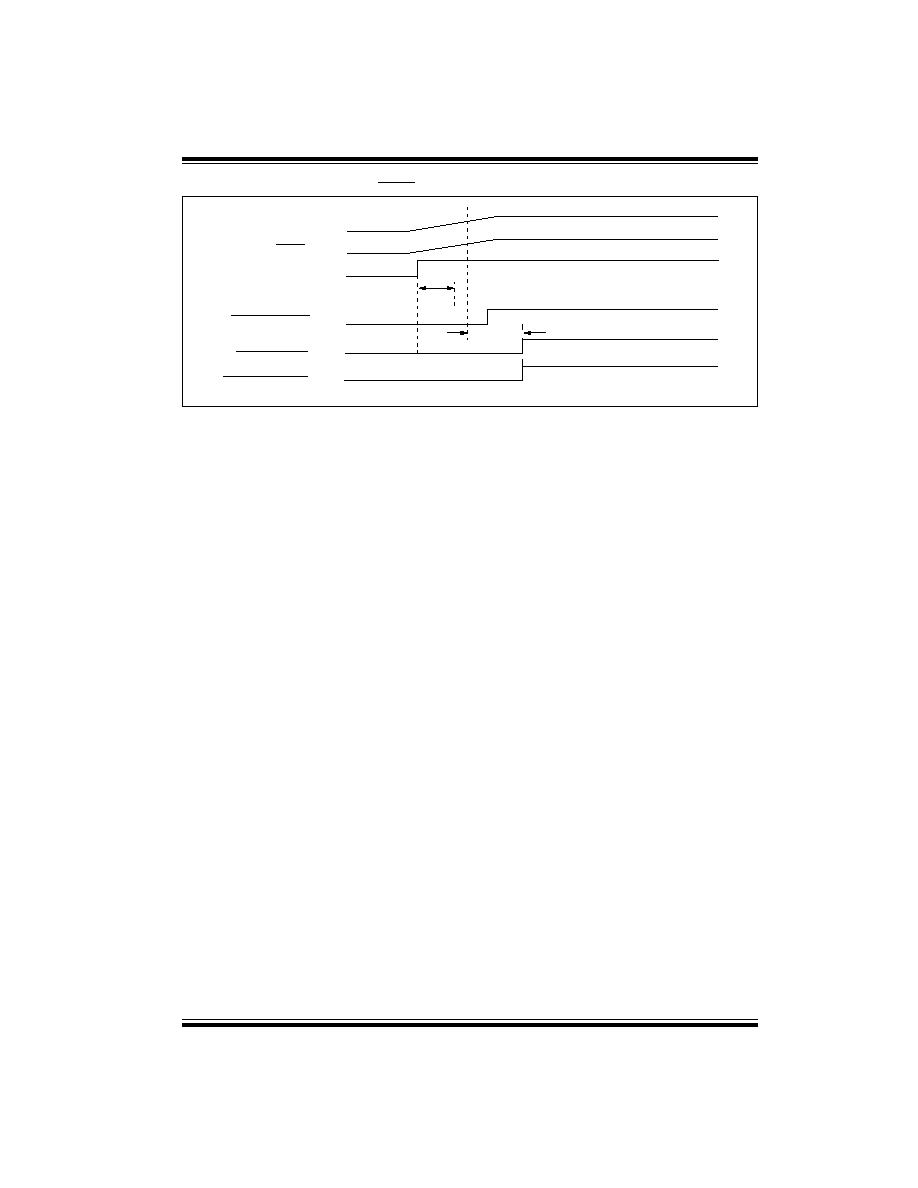
PIC16C72 Series
©
1998 Microchip Technology Inc.
Preliminary
DS39016A-page 67
FIGURE 10-10: SLOW RISE TIME (MCLR TIED TO V
DD
)
V
DD
MCLR
INTERNAL POR
PWRT TIME-OUT
OST TIME-OUT
INTERNAL RESET
0V
1V
5V
T
PWRT
T
OST
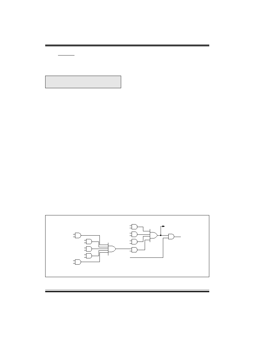
PIC16C72 Series
DS39016A-page 68
Preliminary
©
1998 Microchip Technology Inc.
10.10
Interrupts
The PIC16C72/CR72 has 8 sources of interrupt. The
interrupt control register (INTCON) records individual
interrupt requests in flag bits. It also has individual and
global interrupt enable bits.
A global interrupt enable bit, GIE (INTCON<7>)
enables (if set) all un-masked interrupts or disables (if
cleared) all interrupts. When bit GIE is enabled, and an
interrupt's flag bit and mask bit are set, the interrupt will
vector immediately. Individual interrupts can be dis-
abled through their corresponding enable bits in vari-
ous registers. Individual interrupt bits are set
regardless of the status of the GIE bit. The GIE bit is
cleared on reset.
The "return from interrupt" instruction,
RETFIE
, exits
the interrupt routine as well as sets the GIE bit, which
re-enables interrupts.
The RB0/INT pin interrupt, the RB port change inter-
rupt and the TMR0 overflow interrupt flags are con-
tained in the INTCON register.
The peripheral interrupt flags are contained in the spe-
cial function registers PIR1 and PIR2. The correspond-
ing interrupt enable bits are contained in special
function registers PIE1 and PIE2, and the peripheral
interrupt enable bit is contained in special function reg-
ister INTCON.
When an interrupt is responded to, the GIE bit is
cleared to disable any further interrupt, the return
address is pushed onto the stack and the PC is loaded
with 0004h. Once in the interrupt service routine the
source(s) of the interrupt can be determined by polling
the interrupt flag bits. The interrupt flag bit(s) must be
cleared in software before re-enabling interrupts to
avoid recursive interrupts.
For external interrupt events, such as the INT pin or
PORTB change interrupt, the interrupt latency will be
three or four instruction cycles. The exact latency
depends when the interrupt event occurs. The latency
is the same for one or two cycle instructions. Individual
interrupt flag bits are set regardless of the status of
their corresponding mask bit or the GIE bit
10.10.1 INT INTERRUPT
External interrupt on RB0/INT pin is edge triggered:
either rising if bit INTEDG (OPTION<6>) is set, or fall-
ing, if the INTEDG bit is clear. When a valid edge
appears on the RB0/INT pin, flag bit INTF
(INTCON<1>) is set. This interrupt can be disabled by
clearing enable bit INTE (INTCON<4>). Flag bit INTF
must be cleared in software in the interrupt service rou-
tine before re-enabling this interrupt. The INT interrupt
can wake-up the processor from SLEEP, if bit INTE was
set prior to going into SLEEP. The status of global inter-
rupt enable bit GIE decides whether or not the proces-
sor branches to the interrupt vector following wake-up.
See Section 10.13 for details on SLEEP mode.
10.10.2 TMR0 INTERRUPT
An overflow (FFh
00h) in the TMR0 register will set
flag bit T0IF (INTCON<2>). The interrupt can be
enabled/disabled by setting/clearing enable bit T0IE
(INTCON<5>). (Section 4.0)
10.10.3 PORTB INTCON CHANGE
An input change on PORTB<7:4> sets flag bit RBIF
(INTCON<0>). The interrupt can be enabled/disabled
by setting/clearing enable bit RBIE (INTCON<4>).
(Section 3.2)
FIGURE 10-11: INTERRUPT LOGIC
Note:
Individual interrupt flag bits are set regard-
less of the status of their corresponding
mask bit or the GIE bit.
ADIF
ADIE
SSPIF
SSPIE
CCP1IF
CCP1IE
TMR2IF
TMR2IE
TMR1IF
TMR1IE
T0IF
T0IE
INTF
INTE
RBIF
RBIE
GIE
PEIE
Wake-up (If in SLEEP mode)
Interrupt to CPU
Clear GIE bit

PIC16C72 Series
©
1998 Microchip Technology Inc.
Preliminary
DS39016A-page 69
10.11
Context Saving During Interrupts
During an interrupt, only the return PC value is saved
on the stack. Typically, users may wish to save key reg-
isters during an interrupt, i.e., W register and STATUS
register. This will have to be implemented in software.
Example 10-1 stores and restores the W and STATUS
registers. The register, W_TEMP, must be defined in
each bank and must be defined at the same offset from
the bank base address (i.e., if W_TEMP is defined at
0x20 in bank 0, it must also be defined at 0xA0 in bank
1).
The example:
a)
Stores the W register.
b)
Stores the STATUS register in bank 0.
c)
Executes the ISR code.
d)
Restores the STATUS register (and bank select
bit).
e)
Restores the W register.
EXAMPLE 10-1: SAVING STATUS, W, AND PCLATH REGISTERS IN RAM
MOVWF W_TEMP ;Copy W to W_TEMP register, could be bank one or zero
SWAPF STATUS,W ;Swap status to be saved into W
CLRF STATUS ;bank 0, regardless of current bank, Clears IRP,RP1,RP0
MOVWF STATUS_TEMP ;Save status to bank zero STATUS_TEMP register
:
:
Interrupt Service Routine (ISR) - user defined
:
SWAPF STATUS_TEMP,W ;Swap STATUS_TEMP register into W
;(sets bank to original state)
MOVWF STATUS ;Move W into STATUS register
SWAPF W_TEMP,F ;Swap W_TEMP
SWAPF W_TEMP,W ;Swap W_TEMP into W
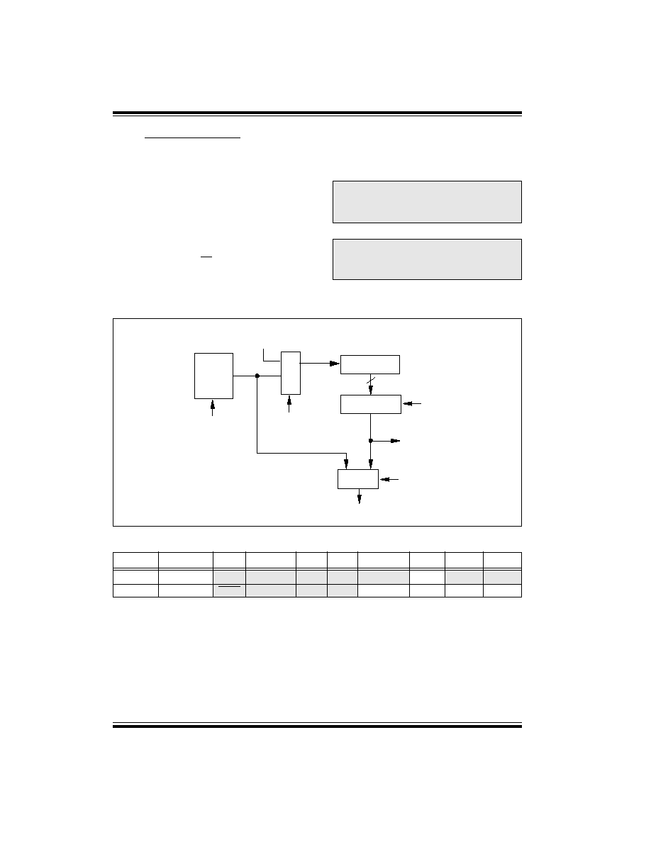
PIC16C72 Series
DS39016A-page 70
Preliminary
©
1998 Microchip Technology Inc.
10.12
Watchdog Timer (WDT)
The Watchdog Timer is as a free running on-chip RC
oscillator which does not require any external compo-
nents. This RC oscillator is separate from the RC oscil-
lator of the OSC1/CLKIN pin. That means that the WDT
will run, even if the clock on the OSC1/CLKIN and
OSC2/CLKOUT pins of the device has been stopped,
for example, by execution of a
SLEEP
instruction.
During normal operation, a WDT time-out generates a
device RESET (Watchdog Timer Reset). If the device is
in SLEEP mode, a WDT time-out causes the device to
wake-up and continue with normal operation (Watch-
dog Timer Wake-up). The TO bit in the STATUS register
will be cleared upon a Watchdog Timer time-out.
The WDT can be permanently disabled by clearing
configuration bit WDTE (Section 10.1).
WDT time-out period values may be found in the Elec-
trical Specifications section under parameter #31. Val-
ues for the WDT prescaler (actually a postscaler, but
shared with the Timer0 prescaler) may be assigned
using the OPTION_REG register.
.
FIGURE 10-12: WATCHDOG TIMER BLOCK DIAGRAM
FIGURE 10-13: SUMMARY OF WATCHDOG TIMER REGISTERS
Note:
The
CLRWDT
and
SLEEP
instructions clear
the WDT and the postscaler, if assigned to
the WDT, and prevent it from timing out
and generating a device RESET condition.
Note:
When a
CLRWDT
instruction is executed
and the prescaler is assigned to the WDT,
the prescaler count will be cleared, but the
prescaler assignment is not changed.
Address
Name
Bit 7
Bit 6
Bit 5
Bit 4
Bit 3
Bit 2
Bit 1
Bit 0
2007h
Config. bits
(1)
BODEN
(1)
CP1
CP0
PWRTE
(1)
WDTE
FOSC1
FOSC0
81h,181h
OPTION
RBPU
INTEDG
T0CS
T0SE
PSA
PS2
PS1
PS0
Legend: Shaded cells are not used by the Watchdog Timer.
Note 1: See Figure 10-1 for operation of these bits.
From TMR0 Clock Source
(Figure 4-2)
To TMR0 (Figure 4-2)
Postscaler
WDT Timer
WDT
Enable Bit
0
1
M
U
X
PSA
8 - to - 1 MUX
PS2:PS0
0
1
MUX
PSA
WDT
Time-out
Note: PSA and PS2:PS0 are bits in the OPTION register.
8

PIC16C72 Series
©
1998 Microchip Technology Inc.
Preliminary
DS39016A-page 71
10.13
Power-down Mode (SLEEP)
Power-down mode is entered by executing a
SLEEP
instruction.
If enabled, the Watchdog Timer will be cleared but
keeps running, the PD bit (STATUS<3>) is cleared, the
TO (STATUS<4>) bit is set, and the oscillator driver is
turned off. The I/O ports maintain the status they had,
before the
SLEEP
instruction was executed (driving
high, low, or hi-impedance).
For lowest current consumption in this mode, place all
I/O pins at either V
DD
, or V
SS
, ensure no external cir-
cuitry is drawing current from the I/O pin, power-down
the A/D, disable external clocks. Pull all I/O pins, that
are hi-impedance inputs, high or low externally to avoid
switching currents caused by floating inputs. The
T0CKI input should also be at V
DD
or V
SS
for lowest
current consumption. The contribution from on-chip
pull-ups on PORTB should be considered.
The MCLR pin must be at a logic high level (V
IHMC
).
10.13.1 WAKE-UP FROM SLEEP
The device can wake up from SLEEP through one of
the following events:
1.
External reset input on MCLR pin.
2.
Watchdog Timer Wake-up (if WDT was
enabled).
3.
Interrupt from INT pin, RB port change, or some
Peripheral Interrupts.
External MCLR Reset will cause a device reset. All
other events are considered a continuation of program
execution and cause a "wake-up". The TO and PD bits
in the STATUS register can be used to determine the
cause of device reset. The PD bit, which is set on
power-up, is cleared when
SLEEP
is invoked. The TO bit
is cleared if a WDT time-out occurred (and caused
wake-up).
The following peripheral interrupts can wake the device
from SLEEP:
1.
TMR1 interrupt. Timer1 must be operating as
an asynchronous counter.
2.
SSP (Start/Stop) bit detect interrupt.
3.
SSP transmit or receive in slave mode (SPI/I
2
C).
4.
CCP capture mode interrupt.
5.
A/D conversion (when A/D clock source is RC).
6.
Special event trigger (Timer1 in asynchronous
mode using an external clock).
Other peripherals cannot generate interrupts since dur-
ing SLEEP, no on-chip clocks are present.
When the
SLEEP
instruction is being executed, the next
instruction (PC + 1) is pre-fetched. For the device to
wake-up through an interrupt event, the corresponding
interrupt enable bit must be set (enabled). Wake-up is
regardless of the state of the GIE bit. If the GIE bit is
clear (disabled), the device continues execution at the
instruction after the
SLEEP
instruction. If the GIE bit is
set (enabled), the device executes the instruction after
the
SLEEP
instruction and then branches to the inter-
rupt address (0004h). In cases where the execution of
the instruction following
SLEEP
is not desirable, the
user should have a
NOP
after the
SLEEP
instruction.
10.13.2 WAKE-UP USING INTERRUPTS
When global interrupts are disabled (GIE cleared) and
any interrupt source has both its interrupt enable bit
and interrupt flag bit set, one of the following will occur:
∑ If the interrupt occurs before the execution of a
SLEEP
instruction, the
SLEEP
instruction will com-
plete as a NOP. Therefore, the WDT and WDT
postscaler will not be cleared, the TO bit will not
be set and PD bits will not be cleared.
∑ If the interrupt occurs during or after the execu-
tion of a
SLEEP
instruction, the device will immedi-
ately wake up from sleep. The
SLEEP
instruction
will be completely executed before the wake-up.
Therefore, the WDT and WDT postscaler will be
cleared, the TO bit will be set and the PD bit will
be cleared.
Even if the flag bits were checked before executing a
SLEEP
instruction, it may be possible for flag bits to
become set before the
SLEEP
instruction completes. To
determine whether a
SLEEP
instruction executed, test
the PD bit. If the PD bit is set, the
SLEEP
instruction was
executed as a NOP.
To ensure that the WDT is cleared, a
CLRWDT
instruc-
tion should be executed before a
SLEEP
instruction.
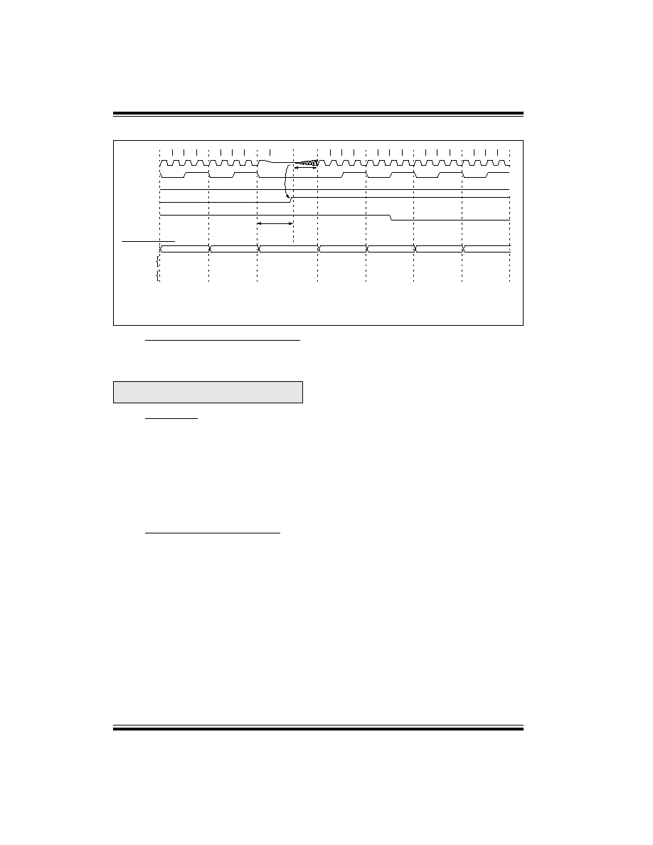
PIC16C72 Series
DS39016A-page 72
Preliminary
©
1998 Microchip Technology Inc.
FIGURE 10-14: WAKE-UP FROM SLEEP THROUGH INTERRUPT
10.14
Program Verification/Code Protection
If the code protection bit(s) have not been pro-
grammed, the on-chip program memory can be read
out for verification purposes.
10.15
ID Locations
Four memory locations (2000h - 2003h) are designated
as ID locations where the user can store checksum or
other code-identification numbers. These locations are
not accessible during normal execution but are read-
able and writable during program/verify. It is recom-
mended that only the 4 least significant bits of the ID
location are used.
For ROM devices, these values are submitted along
with the ROM code.
10.16
In-Circuit Serial ProgrammingTM
PIC16CXXX family microcontrollers can be serially
programmed while in the end application circuit. This is
simply done with two lines for clock and data, and three
other lines for power, ground, and the programming
voltage. This allows customers to manufacture boards
with unprogrammed devices, and then program the
microcontroller just before shipping the product. This
also allows the most recent firmware or a custom firm-
ware to be programmed.
For complete details of serial programming, please
refer to the In-Circuit Serial Programming (ICSPTM)
Guide, DS30277.
Q1
Q2
Q3 Q4
Q1 Q2
Q3
Q4
Q1
Q1
Q2 Q3 Q4
Q1 Q2 Q3 Q4
Q1
Q2 Q3
Q4
Q1 Q2
Q3
Q4
OSC1
CLKOUT(4)
INT pin
INTF flag
(INTCON<1>)
GIE bit
(INTCON<7>)
INSTRUCTION FLOW
PC
Instruction
fetched
Instruction
executed
PC
PC+1
PC+2
Inst(PC) = SLEEP
Inst(PC - 1)
Inst(PC + 1)
SLEEP
Processor in
SLEEP
Interrupt Latency
(Note 2)
Inst(PC + 2)
Inst(PC + 1)
Inst(0004h)
Inst(0005h)
Inst(0004h)
Dummy cycle
PC + 2
0004h
0005h
Dummy cycle
T
OST
(2)
PC+2
Note
1:
XT, HS or LP oscillator mode assumed.
2:
T
OST
= 1024T
OSC
(drawing not to scale) This delay will not be there for RC osc mode.
3:
GIE = '1' assumed. In this case after wake- up, the processor jumps to the interrupt routine. If GIE = '0', execution will continue in-line.
4:
CLKOUT is not available in these osc modes, but shown here for timing reference.
Note:
Microchip does not recommend code pro-
tecting windowed devices.
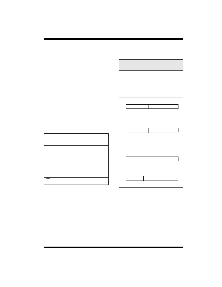
PIC16C72 Series
©
1998 Microchip Technology Inc.
Preliminary
DS39016A-page 73
11.0
INSTRUCTION SET SUMMARY
Each PIC16CXXX family instruction is a 14-bit word
divided into an OPCODE which specifies the instruc-
tion type and one or more operands which further spec-
ify the operation of the instruction. The PIC16CXXX
family instruction set summary in Table 11-2 lists byte-
oriented, bit-oriented, and literal and control opera-
tions. Table 11-1 shows the opcode field descriptions.
For byte-oriented instructions, 'f' represents a file reg-
ister designator and 'd' represents a destination desig-
nator. The file register designator specifies which file
register is to be used by the instruction.
The destination designator specifies where the result of
the operation is to be placed. If 'd' is zero, the result is
placed in the W register. If 'd' is one, the result is placed
in the file register specified in the instruction.
For bit-oriented instructions, 'b' represents a bit field
designator which selects the number of the bit affected
by the operation, while 'f' represents the number of the
file in which the bit is located.
For literal and control operations, 'k' represents an
eight or eleven bit constant or literal value.
TABLE 11-1
OPCODE FIELD
DESCRIPTIONS
The instruction set is highly orthogonal and is grouped
into three basic categories:
∑ Byte-oriented operations
∑ Bit-oriented operations
∑ Literal and control operations
All instructions are executed within one single instruc-
tion cycle, unless a conditional test is true or the pro-
gram counter is changed as a result of an instruction.
In this case, the execution takes two instruction cycles
with the second cycle executed as a NOP. One instruc-
tion cycle consists of four oscillator periods. Thus, for
an oscillator frequency of 4 MHz, the normal instruction
execution time is 1
µ
s. If a conditional test is true or the
program counter is changed as a result of an instruc-
tion, the instruction execution time is 2
µ
s.
Table 11-2 lists the instructions recognized by the
MPASM assembler.
Figure 11-1 shows the general formats that the instruc-
tions can have.
All examples use the following format to represent a
hexadecimal number:
0xhh
where h signifies a hexadecimal digit.
FIGURE 11-1: GENERAL FORMAT FOR
INSTRUCTIONS
A description of each instruction is available in the PIC-
microTM Mid-Range MCU Family Reference Manual,
DS33023.
Field
Description
f
Register file address (0x00 to 0x7F)
W
Working register (accumulator)
b
Bit address within an 8-bit file register
k
Literal field, constant data or label
x
Don't care location (= 0 or 1)
The assembler will generate code with x = 0. It is the
recommended form of use for compatibility with all
Microchip software tools.
d
Destination select; d = 0: store result in W,
d = 1: store result in file register f.
Default is d = 1
PC
Program Counter
TO
Time-out bit
PD
Power-down bit
Note:
To maintain upward compatibility with
future PIC16CXXX products, do not use
the
OPTION
and
TRIS
instructions.
Byte-oriented file register operations
13 8 7 6 0
d = 0 for destination W
OPCODE d f (FILE #)
d = 1 for destination f
f = 7-bit file register address
Bit-oriented file register operations
13 10 9 7 6 0
OPCODE b (BIT #) f (FILE #)
b = 3-bit bit address
f = 7-bit file register address
Literal and control operations
13 8 7 0
OPCODE k (literal)
k = 8-bit immediate value
13 11 10 0
OPCODE k (literal)
k = 11-bit immediate value
General
CALL
and
GOTO
instructions only

PIC16C72 Series
DS39016A-page 74
Preliminary
©
1998 Microchip Technology Inc.
TABLE 11-2
PIC16CXXX INSTRUCTION SET
Mnemonic,
Operands
Description
Cycles
14-Bit Opcode
Status
Affected
Notes
MSb
LSb
BYTE-ORIENTED FILE REGISTER OPERATIONS
ADDWF
ANDWF
CLRF
CLRW
COMF
DECF
DECFSZ
INCF
INCFSZ
IORWF
MOVF
MOVWF
NOP
RLF
RRF
SUBWF
SWAPF
XORWF
f, d
f, d
f
-
f, d
f, d
f, d
f, d
f, d
f, d
f, d
f
-
f, d
f, d
f, d
f, d
f, d
Add W and f
AND W with f
Clear f
Clear W
Complement f
Decrement f
Decrement f, Skip if 0
Increment f
Increment f, Skip if 0
Inclusive OR W with f
Move f
Move W to f
No Operation
Rotate Left f through Carry
Rotate Right f through Carry
Subtract W from f
Swap nibbles in f
Exclusive OR W with f
1
1
1
1
1
1
1(2)
1
1(2)
1
1
1
1
1
1
1
1
1
00
00
00
00
00
00
00
00
00
00
00
00
00
00
00
00
00
00
0111
0101
0001
0001
1001
0011
1011
1010
1111
0100
1000
0000
0000
1101
1100
0010
1110
0110
dfff
dfff
lfff
0xxx
dfff
dfff
dfff
dfff
dfff
dfff
dfff
lfff
0xx0
dfff
dfff
dfff
dfff
dfff
ffff
ffff
ffff
xxxx
ffff
ffff
ffff
ffff
ffff
ffff
ffff
ffff
0000
ffff
ffff
ffff
ffff
ffff
C,DC,Z
Z
Z
Z
Z
Z
Z
Z
Z
C
C
C,DC,Z
Z
1,2
1,2
2
1,2
1,2
1,2,3
1,2
1,2,3
1,2
1,2
1,2
1,2
1,2
1,2
1,2
BIT-ORIENTED FILE REGISTER OPERATIONS
BCF
BSF
BTFSC
BTFSS
f, b
f, b
f, b
f, b
Bit Clear f
Bit Set f
Bit Test f, Skip if Clear
Bit Test f, Skip if Set
1
1
1 (2)
1 (2)
01
01
01
01
00bb
01bb
10bb
11bb
bfff
bfff
bfff
bfff
ffff
ffff
ffff
ffff
1,2
1,2
3
3
LITERAL AND CONTROL OPERATIONS
ADDLW
ANDLW
CALL
CLRWDT
GOTO
IORLW
MOVLW
RETFIE
RETLW
RETURN
SLEEP
SUBLW
XORLW
k
k
k
-
k
k
k
-
k
-
-
k
k
Add literal and W
AND literal with W
Call subroutine
Clear Watchdog Timer
Go to address
Inclusive OR literal with W
Move literal to W
Return from interrupt
Return with literal in W
Return from Subroutine
Go into standby mode
Subtract W from literal
Exclusive OR literal with W
1
1
2
1
2
1
1
2
2
2
1
1
1
11
11
10
00
10
11
11
00
11
00
00
11
11
111x
1001
0kkk
0000
1kkk
1000
00xx
0000
01xx
0000
0000
110x
1010
kkkk
kkkk
kkkk
0110
kkkk
kkkk
kkkk
0000
kkkk
0000
0110
kkkk
kkkk
kkkk
kkkk
kkkk
0100
kkkk
kkkk
kkkk
1001
kkkk
1000
0011
kkkk
kkkk
C,DC,Z
Z
TO
,
PD
Z
TO
,
PD
C,DC,Z
Z
Note 1:
When an I/O register is modified as a function of itself ( e.g.,
MOVF PORTB, 1
), the value used will be that value present
on the pins themselves. For example, if the data latch is '1' for a pin configured as input and is driven low by an external
device, the data will be written back with a '0'.
2: If this instruction is executed on the TMR0 register (and, where applicable, d = 1), the prescaler will be cleared if assigned
to the Timer0 Module.
3: If Program Counter (PC) is modified or a conditional test is true, the instruction requires two cycles. The second cycle is
executed as a NOP.

PIC16C72 Series
©
1998 Microchip Technology Inc.
Preliminary
DS39016A-page 75
12.0
DEVELOPMENT SUPPORT
12.1
Development Tools
The PICmicr
TM
microcontrollers are supported with a
full range of hardware and software development tools:
∑ PICMASTER
Æ
/PICMASTER CE
Real-Time
In-Circuit Emulator
∑ ICEPIC
TM
Low-Cost PIC16C5X and PIC16CXXX
In-Circuit Emulator
∑ PRO MATE
Æ
II Universal Programmer
∑ PICSTART
Æ
Plus Entry-Level Prototype
Programmer
∑ PICDEM-1 Low-Cost Demonstration Board
∑ PICDEM-2 Low-Cost Demonstration Board
∑ PICDEM-3 Low-Cost Demonstration Board
∑ MPASM Assembler
∑ MPLAB
TM
SIM Software Simulator
∑ MPLAB-C17 (C Compiler)
∑ Fuzzy Logic Development System
(
fuzzyTECH
Æ
-
MP)
A description of each development tool is available in
the Midrange Reference Manual, DS33023.
12.2
PICDEM-2 Low-Cost PIC16CXX
Demonstration Board
The PICDEM-2 is a simple demonstration board that
supports the PIC16C62, PIC16C64, PIC16C65,
PIC16C73 and PIC16C74 microcontrollers. All the
necessary hardware and software is included to
run the basic demonstration programs. The user
can program the sample microcontrollers provided
with the PICDEM-2 board, on a PRO MATE II pro-
grammer or PICSTART-Plus, and easily test firmware.
The PICMASTER emulator may also be used with the
PICDEM-2 board to test firmware. Additional prototype
area has been provided to the user for adding addi-
tional hardware and connecting it to the microcontroller
socket(s). Some of the features include a RS-232 inter-
face, push-button switches, a potentiometer for simu-
lated analog input, a Serial EEPROM to demonstrate
usage of the I
2
C bus and separate headers for connec-
tion to an LCD module and a keypad.

PIC16C72 Series
DS39016A-page 76
Preliminary
©
1998 Microchip Technology Inc.
NOTES:
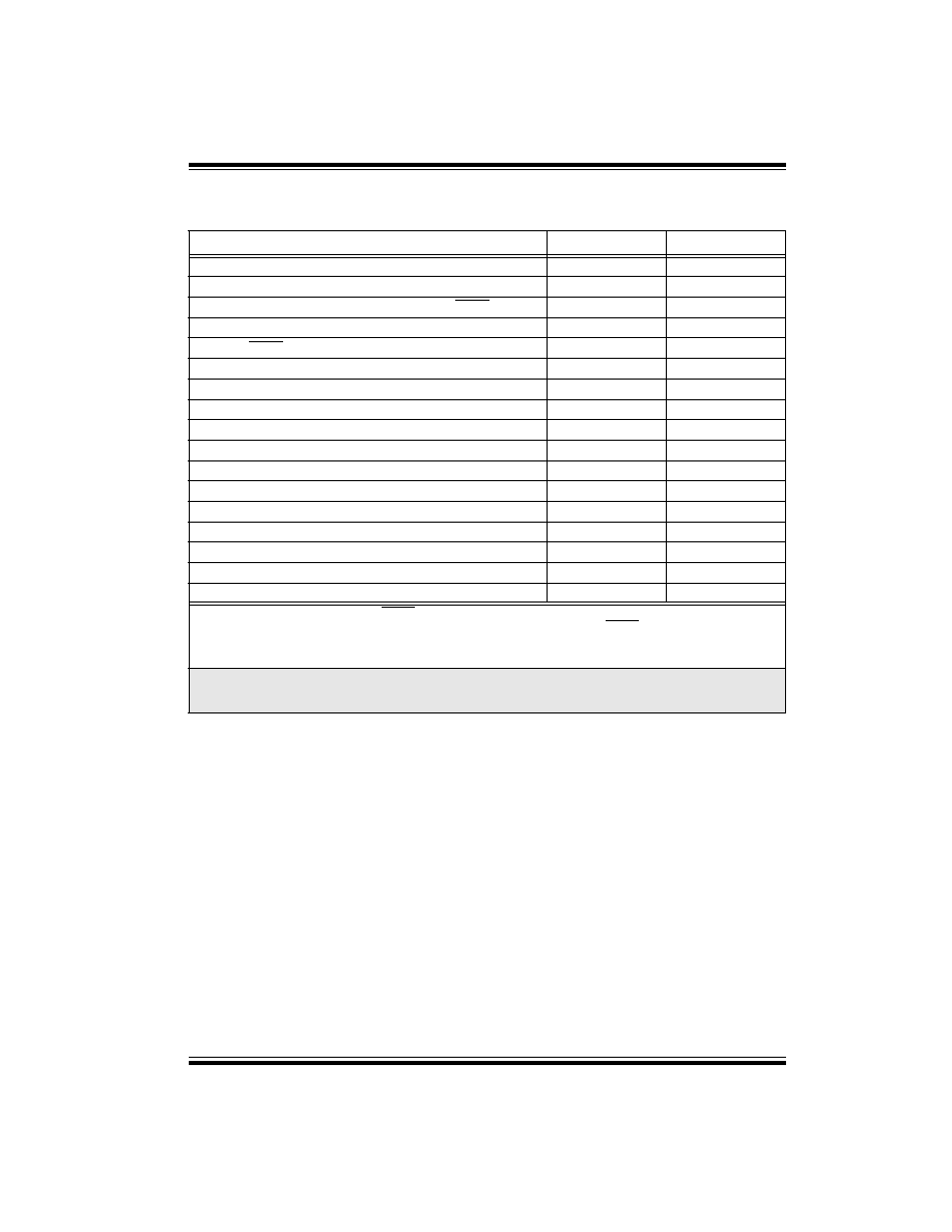
PIC16C72 Series
©
1998 Microchip Technology Inc.
Preliminary
DS39016A-page 77
13.0
ELECTRICAL CHARACTERISTICS - PIC16C72 SERIES
Absolute Maximum Ratings
Parameter
PIC16C72
PIC16CR72
Ambient temperature under bias
-55 to +125∞C
-55 to +125∞C
Storage temperature
-65∞C to +150∞C
-65∞C to +150∞C
Voltage on any pin with respect to V
SS
(except V
DD
, MCLR, and RA4) -0.3V to (V
DD
+ 0.3V)
-0.3V to (V
DD
+ 0.3V)
Voltage on V
DD
with respect to V
SS
-0.3 to +7.5V
TBD
Voltage on MCLR with respect to V
SS
(Note 1)
-0.3 to +14V
TBD
Voltage on RA4 with respect to Vss
-0.3 to +14V
TBD
Total power dissipation (Note 2)
1.0W
1.0W
Maximum current out of V
SS
pin
300 mA
300 mA
Maximum current into V
DD
pin
250 mA
250 mA
Input clamp current, I
IK
(V
I
< 0 or V
I
> V
DD
)
±
20 mA
±
20 mA
Output clamp current, IOK (V
O
< 0 or V
O
> V
DD
)
±
20 mA
±
20 mA
Maximum output current sunk by any I/O pin
25 mA
25 mA
Maximum output current sourced by any I/O pin
25 mA
25 mA
Maximum current sunk by PORTA and PORTB (combined)
200 mA
200 mA
Maximum current sourced by PORTA and PORTB (combined)
200 mA
200 mA
Maximum current sunk by PORTC
200 mA
200 mA
Maximum current sourced by PORTC
200 mA
200 mA
1.
Voltage spikes below V
SS
at the MCLR pin, inducing currents greater than 80 mA, may cause latch-up. Thus,
a series resistor of 50-100
should be used when applying a "low" level to the MCLR pin rather than pulling this
pin directly to V
SS
.
2.
Power dissipation is calculated as follows: Pdis = V
DD
x {I
DD
-
I
OH
} +
{(V
DD
- V
OH
) x I
OH
} +
(V
O
l x I
OL
).
NOTICE: Stresses above those listed under "Absolute Maximum Ratings" may cause permanent damage to the device. This is a
stress rating only and functional operation of the device at those or any other conditions above those indicated in the operation list-
ings of this specification is not implied. Exposure to maximum rating conditions for extended periods may affect device reliability.
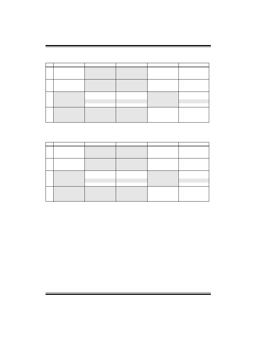
PIC16C72 Series
DS39016A-page 78
Preliminary
©
1998 Microchip Technology Inc.
TABLE 13-1
CROSS REFERENCE OF DEVICE SPECS (PIC16C72) FOR OSCILLATOR
CONFIGURATIONS AND FREQUENCIES OF OPERATION (COMMERCIAL DEVICES)
TABLE 13-2
CROSS REFERENCE OF DEVICE SPECS (PIC16CR72) FOR OSCILLATOR
CONFIGURATIONS AND FREQUENCIES OF OPERATION (COMMERCIAL DEVICES)
OSC
PIC16C72-04
PIC16C72-10
PIC16C72-20
PIC16LC72-04
JW Devices
RC
V
DD
: 4.0V to 6.0V
I
DD
: 5 mA max. at 5.5V
I
PD
: 16
µ
A max. at 4V
Freq: 4 MHz max.
V
DD
: 4.5V to 5.5V
I
DD
: 2.7 mA typ. at 5.5V
I
PD
: 1.5
µ
A typ. at 4V
Freq: 4 MHz max.
V
DD
: 4.5V to 5.5V
I
DD
: 2.7 mA typ. at 5.5V
I
PD
: 1.5
µ
A typ. at 4V
Freq: 4 MHz max.
V
DD
: 2.5V to 6.0V
I
DD
: 3.8 mA max. at 3.0V
I
PD
: 5.0
µ
A max. at 3V
Freq: 4 MHz max.
V
DD
: 4.0V to 6.0V
I
DD
: 5 mA max. at 5.5V
I
PD
: 16
µ
A max. at 4V
Freq: 4 MHz max.
XT
V
DD
: 4.0V to 6.0V
I
DD
: 5 mA max. at 5.5V
I
PD
: 16
µ
A max. at 4V
Freq: 4 MHz max.
V
DD
: 4.5V to 5.5V
I
DD
: 2.7 mA typ. at 5.5V
I
PD
: 1.5
µ
A typ. at 4V
Freq: 4 MHz max.
V
DD
: 4.5V to 5.5V
I
DD
: 2.7 mA typ. at 5.5V
I
PD
: 1.5
µ
A typ. at 4V
Freq: 4 MHz max.
V
DD
: 2.5V to 6.0V
I
DD
: 3.8 mA max. at 3.0V
I
PD
: 5.0
µ
A max. at 3V
Freq: 4 MHz max.
V
DD
: 4.0V to 6.0V
I
DD
: 5 mA max. at 5.5V
I
PD
: 16
µ
A max. at 4V
Freq: 4 MHz max.
HS
V
DD
: 4.5V to 5.5V
V
DD
: 4.5V to 5.5V
V
DD
: 4.5V to 5.5V
Not recommended for use
in HS mode
V
DD
: 4.5V to 5.5V
I
DD
: 13.5 mA typ. at 5.5V
I
DD
: 10 mA max. at 5.5V
I
DD
: 20 mA max. at 5.5V
I
DD
: 20 mA max. at 5.5V
I
PD
: 1.5
µ
A typ. at 4.5V
I
PD
: 1.5
µ
A typ. at 4.5V
I
PD
: 1.5
µ
A typ. at 4.5V
I
PD
: 1.5
µ
A typ. at 4.5V
Freq: 4 MHz max.
Freq: 10 MHz max.
Freq: 20 MHz max.
Freq: 20 MHz max.
LP
V
DD
: 4.0V to 6.0V
I
DD
: 52.5
µ
A typ. at
32 kHz, 4.0V
I
PD
: 0.9
µ
A typ. at 4.0V
Freq: 200 kHz max.
Not recommended for use
in LP mode
Not recommended for use
in LP mode
V
DD
: 2.5V to 6.0V
I
DD
: 48
µ
A max. at
32 kHz, 3.0V
I
PD
: 5.0
µ
A max. at 3.0V
Freq: 200 kHz max.
V
DD
: 2.5V to 6.0V
I
DD
: 48
µ
A max. at
32 kHz, 3.0V
I
PD
: 5.0
µ
A max. at 3.0V
Freq: 200 kHz max.
The shaded sections indicate oscillator selections which are tested for functionality, but not for MIN/MAX specifications.
It is recommended that the user select the device type that ensures the specifications required.
OSC
PIC16CR72-04
PIC16CR72-10
PIC16CR72-20
PIC16LCR72-04
JW Devices
RC
V
DD
: 4.0V to 5.5V
I
DD
: 5 mA max. at 5.5V
I
PD
: 16
µ
A max. at 4V
Freq: 4 MHz max.
V
DD
: 4.5V to 5.5V
I
DD
: 2.7 mA typ. at 5.5V
I
PD
: 1.5
µ
A typ. at 4V
Freq: 4 MHz max.
V
DD
: 4.5V to 5.5V
I
DD
: 2.7 mA typ. at 5.5V
I
PD
: 1.5
µ
A typ. at 4V
Freq: 4 MHz max.
V
DD
: 2.5V to 5.5V
I
DD
: 3.8 mA max. at 3.0V
I
PD
: 5.0
µ
A max. at 3V
Freq: 4 MHz max.
V
DD
: 4.0V to 5.5V
I
DD
: 5 mA max. at 5.5V
I
PD
: 16
µ
A max. at 4V
Freq: 4 MHz max.
XT
V
DD
: 4.0V to 5.5V
I
DD
: 5 mA max. at 5.5V
I
PD
: 16
µ
A max. at 4V
Freq: 4 MHz max.
V
DD
: 4.5V to 5.5V
I
DD
: 2.7 mA typ. at 5.5V
I
PD
: 1.5
µ
A typ. at 4V
Freq: 4 MHz max.
V
DD
: 4.5V to 5.5V
I
DD
: 2.7 mA typ. at 5.5V
I
PD
: 1.5
µ
A typ. at 4V
Freq: 4 MHz max.
V
DD
: 2.5V to 5.5V
I
DD
: 3.8 mA max. at 3.0V
I
PD
: 5.0
µ
A max. at 3V
Freq: 4 MHz max.
V
DD
: 4.0V to 5.5V
I
DD
: 5 mA max. at 5.5V
I
PD
: 16
µ
A max. at 4V
Freq: 4 MHz max.
HS
V
DD
: 4.5V to 5.5V
V
DD
: 4.5V to 5.5V
V
DD
: 4.5V to 5.5V
Not recommended for use
in HS mode
V
DD
: 4.5V to 5.5V
I
DD
: 13.5 mA typ. at 5.5V
I
DD
: 10 mA max. at 5.5V
I
DD
: 20 mA max. at 5.5V
I
DD
: 20 mA max. at 5.5V
I
PD
: 1.5
µ
A typ. at 4.5V
I
PD
: 1.5
µ
A typ. at 4.5V
I
PD
: 1.5
µ
A typ. at 4.5V
I
PD
: 1.5
µ
A typ. at 4.5V
Freq: 4 MHz max.
Freq: 10 MHz max.
Freq: 20 MHz max.
Freq: 20 MHz max.
LP
V
DD
: 4.0V to 5.5V
I
DD
: 52.5
µ
A typ. at
32 kHz, 4.0V
I
PD
: 0.9
µ
A typ. at 4.0V
Freq: 200 kHz max.
Not recommended for use
in LP mode
Not recommended for use
in LP mode
V
DD
: 2.5V to 5.5V
I
DD
: 48
µ
A max. at
32 kHz, 3.0V
I
PD
: 5.0
µ
A max. at 3.0V
Freq: 200 kHz max.
V
DD
: 2.5V to 5.5V
I
DD
: 48
µ
A max. at
32 kHz, 3.0V
I
PD
: 5.0
µ
A max. at 3.0V
Freq: 200 kHz max.
The shaded sections indicate oscillator selections which are tested for functionality, but not for MIN/MAX specifications.
It is recommended that the user select the device type that ensures the specifications required.
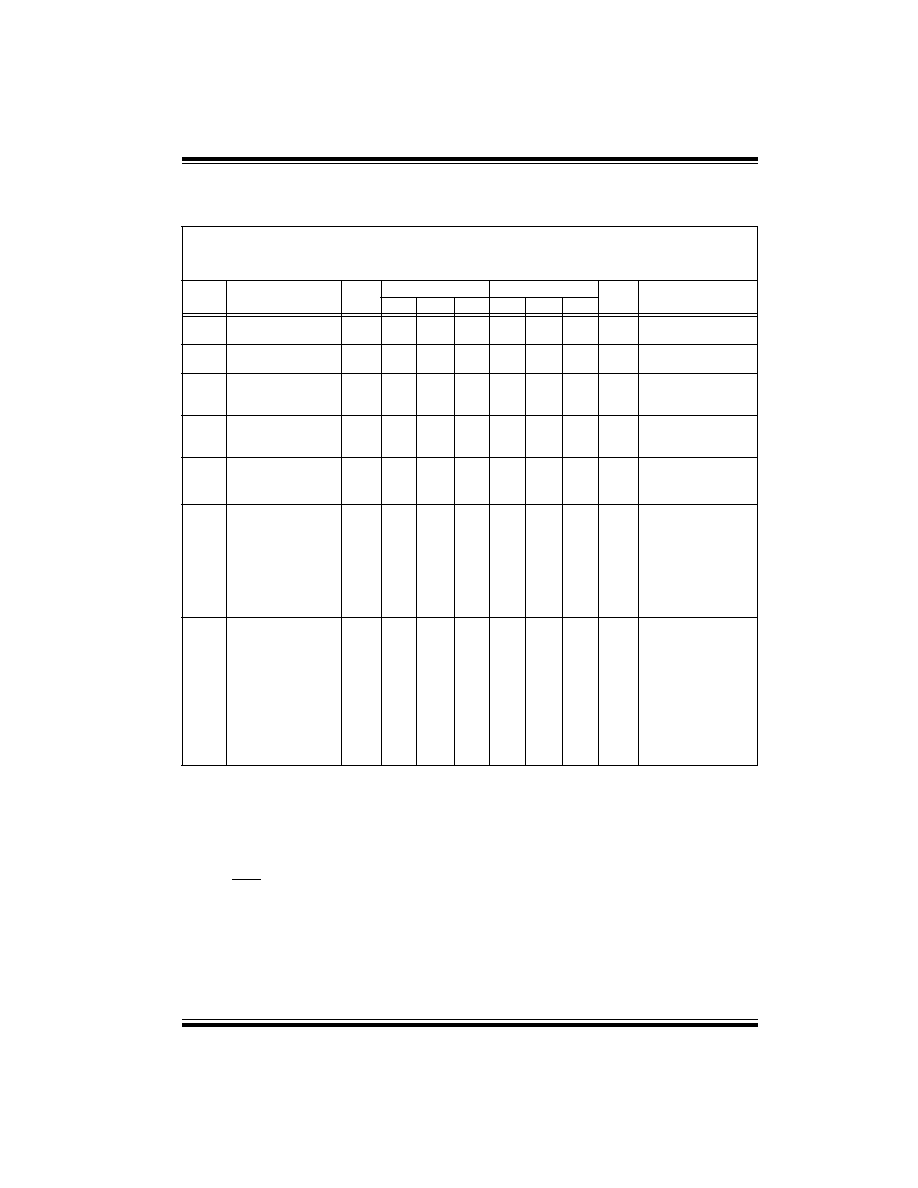
PIC16C72 Series
©
1998 Microchip Technology Inc.
Preliminary
DS39016A-page 79
13.1
DC Characteristics:
PIC16C72/CR72-04 (Commercial, Industrial, Extended)
PIC16C72/CR72-10 (Commercial, Industrial, Extended)
PIC16C72/CR72-20 (Commercial, Industrial, Extended)
DC CHARACTERISTICS
Standard Operating Conditions (unless otherwise stated)
Operating temperature
-40∞C
T
A
+125∞C for extended,
-40∞C
T
A
+85∞C for industrial and
0∞C
T
A
+70∞C for commercial
Param
No.
Characteristic
Sym
PIC16C72
PIC16CR72
Units
Conditions
Min
Typ
Max
Min
Typ
Max
D001
D001A
Supply Voltage
V
DD
4.0
4.5
-
-
6.0
5.5
4.0
4.5
-
-
5.5
5.5
V
V
XT, RC and LP osc
HS osc
D002*
RAM Data Retention
Voltage (Note 1)
V
DR
-
1.5
-
-
1.5
-
V
D003
V
DD
start voltage to
ensure internal Power-
on Reset Signal
V
POR
-
V
SS
-
-
V
SS
-
V
See section on Power-
on Reset for details
D004*
V
DD
rise rate to ensure
internal Power-on
Reset Signal
S
VDD
0.05
-
-
0.05
-
-
V/ms
See section on Power-
on Reset for details
D005
Brown-out Reset Volt-
age
Bvdd
3.7
4.0
4.3
3.7
4.0
4.3
V
BODEN bit in configura-
tion word enabled
3.7
4.0
4.4
3.7
4.0
4.4
V
Extended Only
D010
Supply Current
(Note 2,5)
I
DD
-
2.7
5.0
-
2.7
5.0
mA
XT, RC osc
F
OSC
= 4 MHz,
V
DD
= 5.5V (Note 4)
D013
-
10
20
-
10
20
mA
HS osc
F
OSC
= 20 MHz,
V
DD
= 5.5V
D015
Brown-out Reset
Current (Note 6)
Ibor
-
350
425
-
350
425
µ
A
BOR enabled,
V
DD
= 5.0V
D020
Power-down Current
(Note 3,5)
I
PD
-
10.5
42
-
10.5
42
µ
A
V
DD
= 4.0V, WDT
enabled, -40
∞
C to +85
∞
C
D021
-
1.5
16
-
1.5
16
µ
A
V
DD
= 4.0V, WDT dis-
abled, -0
∞
C to +70
∞
C
D021A
-
1.5
19
-
1.5
19
µ
A
V
DD
= 4.0V, WDT dis-
abled, -40
∞
C to +85
∞
C
D021B
-
2.5
19
-
2.5
19
µ
A
V
DD
= 4.0V, WDT dis-
abled, -40
∞
C to +125
∞
C
D023
Brown-out Reset
Current (Note 6)
Ibor
-
350
425
-
350
425
µ
A
BOR enabled V
DD
=
5.0V
*
These parameters are characterized but not tested.
Data in "Typ" column is at 5V, 25∞C unless otherwise stated. These parameters are for design guidance only and are not
tested.
Note 1:
This is the limit to which V
DD
can be lowered without losing RAM data.
Note 2:
The supply current is mainly a function of the operating voltage and frequency. Other factors such as I/O pin loading and
switching rate, oscillator type, internal code execution pattern, and temperature also have an impact on the current con-
sumption.
The test conditions for all I
DD
measurements in active operation mode are:
OSC1 = external square wave, from rail to rail; all I/O pins tristated, pulled to V
DD
MCLR = V
DD
; WDT enabled/disabled as specified.
Note 3:
The power-down current in SLEEP mode does not depend on the oscillator type. Power-down current is measured with
the part in SLEEP mode, with all I/O pins in hi-impedance state and tied to V
DD
and V
SS
.
Note 4:
For RC osc configuration, current through Rext is not included. The current through the resistor can be estimated by the
formula Ir = V
DD
/2Rext (mA) with Rext in kOhm.
Note 5:
Timer1 oscillator (when enabled) adds approximately 20
µ
A to the specification. This value is from characterization and
is for design guidance only. This is not tested.
Note 6:
The
current is the additional current consumed when this peripheral is enabled. This current should be added to the
base I
DD
or I
PD
measurement.
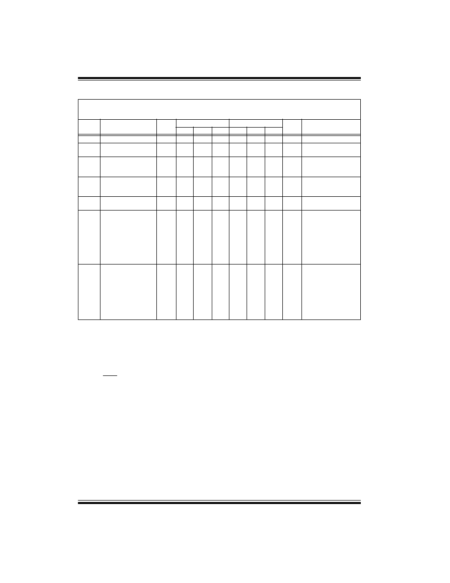
PIC16C72 Series
DS39016A-page 80
Preliminary
©
1998 Microchip Technology Inc.
13.2
DC Characteristics:
PIC16LC72/LCR72-04 (Commercial, Industrial)
DC CHARACTERISTICS
Standard Operating Conditions (unless otherwise stated)
Operating temperature
-40∞C
T
A
+85∞C for industrial and
0∞C
T
A
+70∞C for commercial
Param
No.
Characteristic
Sym
PIC16C72
PIC16CR72
Units
Conditions
Min
Typ
Max
Min
Typ
Max
D001
Supply Voltage
V
DD
2.5
-
6.0
2.5
-
5.5
V
LP, XT, RC (DC - 4 MHz)
D002*
RAM Data Retention
Voltage (Note 1)
V
DR
-
1.5
-
-
1.5
-
V
D003
V
DD
start voltage to
ensure internal Power-
on Reset signal
V
POR
-
V
SS
-
-
V
SS
-
V
See section on Power-
on Reset for details
D004*
V
DD
rise rate to ensure
internal Power-on
Reset signal
S
VDD
0.05
-
-
0.05
-
-
V/ms
See section on Power-
on Reset for details
D005
Brown-out Reset Volt-
age
Bvdd
3.7
4.0
4.3
3.7
4.0
4.3
V
BODEN bit in configura-
tion word enabled
D010
Supply Current
(Note 2,5)
I
DD
-
2.0
3.8
-
2.0
3.8
mA
XT, RC osc configuration
F
OSC
= 4 MHz, V
DD
=
3.0V (Note 4)
D010A
-
22.5
48
-
22.5
48
µ
A
LP osc configuration
F
OSC
= 32 kHz, V
DD
=
3.0V, WDT disabled
D015*
Brown-out Reset
Current (Note 6)
Ibor
-
350
425
-
350
425
µ
A
BOR enabled V
DD
=
5.0V
D020
Power-down Current
(Note 3,5)
I
PD
-
7.5
30
-
7.5
30
µ
A
V
DD
= 3.0V, WDT
enabled, -40
∞
C to +85
∞
C
D021
-
0.9
5
-
0.9
5
µ
A
V
DD
= 3.0V, WDT dis-
abled, 0
∞
C to +70
∞
C
D021A
-
0.9
5
-
0.9
5
µ
A
V
DD
= 3.0V, WDT dis-
abled, -40
∞
C to +85
∞
C
D023*
Brown-out Reset
Current (Note 6)
Ibor
-
350
425
-
350
425
µ
A
BOR enabled V
DD
=
5.0V
*
These parameters are characterized but not tested.
Data in "Typ" column is at 5V, 25∞C unless otherwise stated. These parameters are for design guidance only and are not
tested.
Note 1:
This is the limit to which V
DD
can be lowered without losing RAM data.
Note 2:
The supply current is mainly a function of the operating voltage and frequency. Other factors such as I/O pin loading and
switching rate, oscillator type, internal code execution pattern, and temperature also have an impact on the current con-
sumption.
The test conditions for all I
DD
measurements in active operation mode are:
OSC1 = external square wave, from rail to rail; all I/O pins tristated, pulled to V
DD
MCLR = V
DD
; WDT enabled/disabled as specified.
Note 3:
The power-down current in SLEEP mode does not depend on the oscillator type. Power-down current is measured with
the part in SLEEP mode, with all I/O pins in hi-impedance state and tied to V
DD
and V
SS
.
Note 4:
For RC osc configuration, current through Rext is not included. The current through the resistor can be estimated by the
formula Ir = V
DD
/2Rext (mA) with Rext in kOhm.
Note 5:
Timer1 oscillator (when enabled) adds approximately 20
µ
A to the specification. This value is from characterization and
is for design guidance only. This is not tested.
Note 6:
The
current is the additional current consumed when this peripheral is enabled. This current should be added to the
base I
DD
or I
PD
measurement.
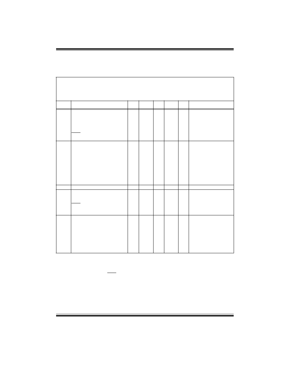
PIC16C72 Series
©
1998 Microchip Technology Inc.
Preliminary
DS39016A-page 81
13.3
DC Characteristics:
PIC16C72/CR72-04 (Commercial, Industrial, Extended)
PIC16C72/CR72-10 (Commercial, Industrial, Extended)
PIC16C72/CR72-20 (Commercial, Industrial, Extended)
PIC16LC72/LCR72-04 (Commercial, Industrial)
DC CHARACTERISTICS
Standard Operating Conditions (unless otherwise stated)
Operating temperature
-40∞C
T
A
+125∞C for extended,
-40∞C
T
A
+85∞C for industrial and
0∞C
T
A
+70∞C for commercial
Operating voltage V
DD
range as described in DC spec Section 13.1 and
Section 13.2.
Param
No.
Characteristic
Sym
Min
Typ
Max
Units
Conditions
Input Low Voltage
I/O ports
V
IL
D030
with TTL buffer
V
SS
-
0.15V
DD
V
For entire V
DD
range
D030A
Vss
-
0.8V
V
4.5
V
DD
5.5V
D031
with Schmitt Trigger buffer
V
SS
-
0.2V
DD
V
D032
MCLR, OSC1 (in RC mode)
V
SS
-
0.2V
DD
V
D033
OSC1 (in XT, HS and LP)
V
SS
-
0.3V
DD
V
Note1
Input High Voltage
I/O ports
V
IH
-
D040
with TTL buffer
2.0
-
V
DD
V
4.5
V
DD
5.5V
D040A
0.25V
DD
+
0.8V
-
V
DD
V
For entire V
DD
range
D041
with Schmitt Trigger buffer
0.8V
DD
-
V
DD
V
For entire V
DD
range
D042
MCLR
0.8V
DD
-
V
DD
V
D042A
OSC1 (XT, HS and LP)
0.7V
DD
-
Vdd
V
Note1
D043
OSC1 (in RC mode)
0.9V
DD
-
V
DD
V
D070
PORTB weak pull-up current
I
PURB
50
250
400
µ
A
V
DD
= 5V, V
PIN
= V
SS
Input Leakage Current (Notes 2, 3)
D060
I/O ports
I
IL
-
-
±
1
µ
A
Vss
V
PIN
V
DD
, Pin at hi-
impedance
D061
MCLR, RA4/T0CKI
-
-
±
5
µ
A
Vss
V
PIN
V
DD
D063
OSC1
-
-
±
5
µ
A
Vss
V
PIN
V
DD
, XT, HS and LP
osc configuration
Output Low Voltage
D080
I/O ports
V
OL
-
-
0.6
V
I
OL
= 8.5 mA, V
DD
= 4.5V,
-40
∞
C to +85
∞
C
D080A
-
-
0.6
V
I
OL
= 7.0 mA, V
DD
= 4.5V,
-40
∞
C to +125
∞
C
D083
OSC2/CLKOUT (RC osc config)
-
-
0.6
V
I
OL
= 1.6 mA, V
DD
= 4.5V,
-40
∞
C to +85
∞
C
D083A
-
-
0.6
V
I
OL
= 1.2 mA, V
DD
= 4.5V,
-40
∞
C to +125
∞
C
*
These parameters are characterized but not tested.
Data in "Typ" column is at 5V, 25
∞
C unless otherwise stated. These parameters are for design guidance only and are not
tested.
Note 1:
In RC oscillator configuration, the OSC1/CLKIN pin is a Schmitt trigger input. It is not recommended that the PIC16C7X be
driven with external clock in RC mode.
Note 2:
The leakage current on the MCLR/V
PP
pin is strongly dependent on the applied voltage level. The specified levels repre-
sent normal operating conditions. Higher leakage current may be measured at different input voltages.
Note 3:
Negative current is defined as current sourced by the pin.
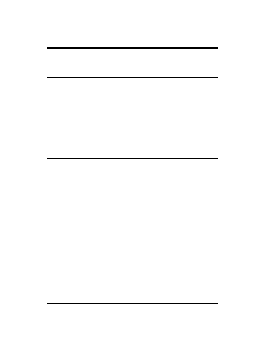
PIC16C72 Series
DS39016A-page 82
Preliminary
©
1998 Microchip Technology Inc.
Output High Voltage
D090
I/O ports (Note 3)
V
OH
V
DD
- 0.7
-
-
V
I
OH
= -3.0 mA, V
DD
= 4.5V,
-40
∞
C to +85
∞
C
D090A
V
DD
- 0.7
-
-
V
I
OH
= -2.5 mA, V
DD
= 4.5V,
-40
∞
C to +125
∞
C
D092
OSC2/CLKOUT (RC osc config)
V
DD
- 0.7
-
-
V
I
OH
= -1.3 mA, V
DD
= 4.5V,
-40
∞
C to +85
∞
C
D092A
V
DD
- 0.7
-
-
V
I
OH
= -1.0 mA, V
DD
= 4.5V,
-40
∞
C to +125
∞
C
D150*
Open-Drain High Voltage
Vod
-
-
14
V
RA4 pin, PIC16C72/LC72
-
-
TBD
V
RA4 pin, PIC16CR72/LCR72
Capacitive Loading Specs on Output
Pins
D100
OSC2 pin
C
OSC2
-
-
15
pF
In XT, HS and LP modes when
external clock is used to drive
OSC1.
D101
D102
All I/O pins and OSC2 (in RC mode)
SCL, SDA in I
2
C mode
C
IO
Cb
-
-
-
-
50
400
pF
pF
DC CHARACTERISTICS
Standard Operating Conditions (unless otherwise stated)
Operating temperature
-40∞C
T
A
+125∞C for extended,
-40∞C
T
A
+85∞C for industrial and
0∞C
T
A
+70∞C for commercial
Operating voltage V
DD
range as described in DC spec Section 13.1 and
Section 13.2.
Param
No.
Characteristic
Sym
Min
Typ
Max
Units
Conditions
*
These parameters are characterized but not tested.
Data in "Typ" column is at 5V, 25
∞
C unless otherwise stated. These parameters are for design guidance only and are not
tested.
Note 1:
In RC oscillator configuration, the OSC1/CLKIN pin is a Schmitt trigger input. It is not recommended that the PIC16C7X be
driven with external clock in RC mode.
Note 2:
The leakage current on the MCLR/V
PP
pin is strongly dependent on the applied voltage level. The specified levels repre-
sent normal operating conditions. Higher leakage current may be measured at different input voltages.
Note 3:
Negative current is defined as current sourced by the pin.
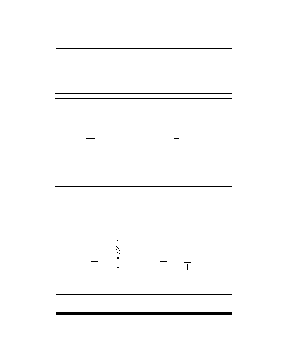
PIC16C72 Series
©
1998 Microchip Technology Inc.
Preliminary
DS39016A-page 83
13.4
Timing Parameter Symbology
The timing parameter symbols have been created fol-
lowing one of the following formats:
FIGURE 13-1: LOAD CONDITIONS
1. TppS2ppS
3. T
CC
:
ST
(I
2
C specifications only)
2. TppS
4. Ts
(I
2
C specifications only)
T
F
Frequency
T
Time
Lowercase letters (pp) and their meanings:
pp
cc
CCP1
osc
OSC1
ck
CLKOUT
rd
RD
cs
CS
rw
RD or WR
di
SDI
sc
SCK
do
SDO
ss
SS
dt
Data in
t0
T0CKI
io
I/O port
t1
T1CKI
mc
MCLR
wr
WR
Uppercase letters and their meanings:
S
F
Fall
P
Period
H
High
R
Rise
I
Invalid (Hi-impedance)
V
Valid
L
Low
Z
Hi-impedance
I
2
C only
AA
output access
High
High
BUF
Bus free
Low
Low
T
CC
:
ST
(I
2
C specifications only)
CC
HD
Hold
SU
Setup
ST
DAT
DATA input hold
STO
STOP condition
STA
START condition
V
DD
/2
C
L
R
L
Pin
Pin
V
SS
V
SS
C
L
R
L
= 464
C
L
= 50 pF
for all pins except OSC2
15 pF
for OSC2 output
Load condition 1
Load condition 2
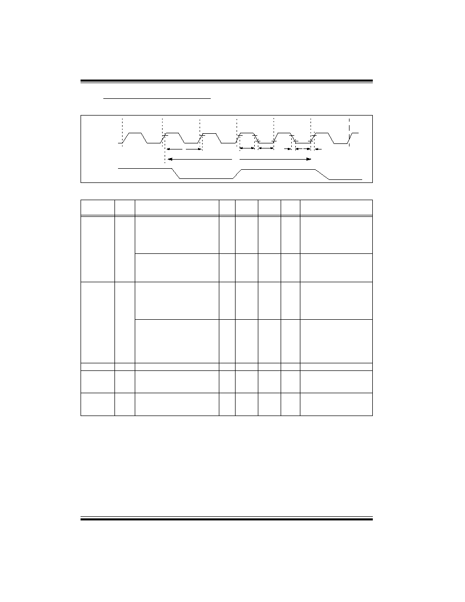
PIC16C72 Series
DS39016A-page 84
Preliminary
©
1998 Microchip Technology Inc.
13.5
Timing Diagrams and Specifications
FIGURE 13-2: EXTERNAL CLOCK TIMING
OSC1
CLKOUT
Q4
Q1
Q2
Q3
Q4
Q1
1
2
3
3
4
4
TABLE 13-3
EXTERNAL CLOCK TIMING REQUIREMENTS
Parameter
No.
Sym
Characteristic
Min
Typ
Max
Units
Conditions
Fosc
External CLKIN Frequency
(Note 1)
DC
--
4
MHz
XT and RC osc mode
DC
--
4
MHz
HS osc mode (-04)
DC
--
10
MHz
HS osc mode (-10)
DC
--
20
MHz
HS osc mode (-20)
DC
--
200
kHz
LP osc mode
Oscillator Frequency
(Note 1)
DC
--
4
MHz
RC osc mode
0.1
--
4
MHz
XT osc mode
4
5
--
--
20
200
MHz
kHz
HS osc mode
LP osc mode
1
Tosc
External CLKIN Period
(Note 1)
250
--
--
ns
XT and RC osc mode
250
--
--
ns
HS osc mode (-04)
100
--
--
ns
HS osc mode (-10)
50
--
--
ns
HS osc mode (-20)
5
--
--
µ
s
LP osc mode
Oscillator Period
(Note 1)
250
--
--
ns
RC osc mode
250
--
10,000
ns
XT osc mode
250
--
250
ns
HS osc mode (-04)
100
50
--
--
250
250
ns
ns
HS osc mode (-10)
HS osc mode (-20)
5
--
--
µ
s
LP osc mode
2
T
CY
Instruction Cycle Time (Note 1)
200
--
DC
ns
T
CY
= 4/F
OSC
3
TosL,
TosH
External Clock in (OSC1) High or
Low Time
100
--
--
ns
XT oscillator
2.5
--
--
µ
s
LP oscillator
15
--
--
ns
HS oscillator
4
TosR,
TosF
External Clock in (OSC1) Rise or
Fall Time
--
--
25
ns
XT oscillator
--
--
50
ns
LP oscillator
--
--
15
ns
HS oscillator
Data in "Typ" column is at 5V, 25∞C unless otherwise stated. These parameters are for design guidance only and are not
tested.
Note 1:
Instruction cycle period (T
CY
) equals four times the input oscillator time-base period. All specified values are based on
characterization data for that particular oscillator type under standard operating conditions with the device executing
code. Exceeding these specified limits may result in an unstable oscillator operation and/or higher than expected current
consumption. All devices are tested to operate at "min." values with an external clock applied to the OSC1/CLKIN pin.
When an external clock input is used, the "Max." cycle time limit is "DC" (no clock) for all devices.
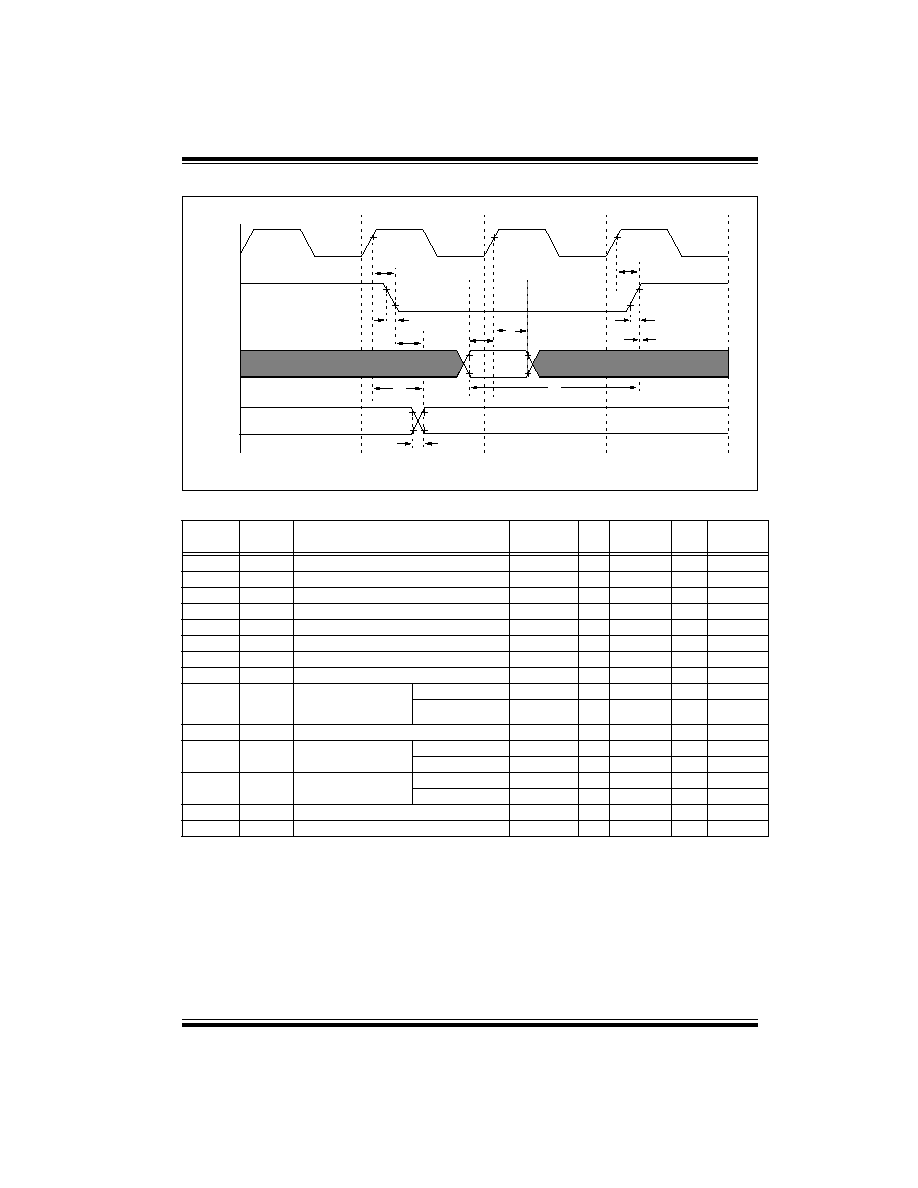
PIC16C72 Series
©
1998 Microchip Technology Inc.
Preliminary
DS39016A-page 85
FIGURE 13-3: CLKOUT AND I/O TIMING
TABLE 13-4
CLKOUT AND I/O TIMING REQUIREMENTS
Parameter
No.
Sym
Characteristic
Min
Typ
Max
Units
Conditions
10*
TosH2ckL
OSC1
to CLKOUT
--
75
200
ns
Note 1
11*
TosH2ckH
OSC1
to CLKOUT
--
75
200
ns
Note 1
12*
TckR
CLKOUT rise time
--
35
100
ns
Note 1
13*
TckF
CLKOUT fall time
--
35
100
ns
Note 1
14*
TckL2ioV
CLKOUT
to Port out valid
--
--
0.5T
CY
+ 20
ns
Note 1
15*
TioV2ckH
Port in valid before CLKOUT
T
OSC
+ 200
--
--
ns
Note 1
16*
TckH2ioI
Port in hold after CLKOUT
0
--
--
ns
Note 1
17*
TosH2ioV
OSC1
(Q1 cycle) to Port out valid
--
50
150
ns
18*
TosH2ioI
OSC1
(Q2 cycle) to
Port input invalid (I/O in
hold time)
PIC16C72/CR72
100
--
--
ns
PIC16LC72/LCR72
200
--
--
ns
19*
TioV2osH
Port input valid to OSC1
(I/O in setup time)
0
--
--
ns
20*
TioR
Port output rise time
PIC16C72/CR72
--
10
40
ns
PIC16LC72/LCR72
--
--
80
ns
21*
TioF
Port output fall time
PIC16C72/CR72
--
10
40
ns
PIC16LC72/LCR72
--
--
80
ns
22*
Tinp
INT pin high or low time
T
CY
--
--
ns
23*
Trbp
RB7:RB4 change INT high or low time
T
CY
--
--
ns
*
These parameters are characterized but not tested.
Data in "Typ" column is at 5V, 25∞C unless otherwise stated. These parameters are for design guidance
only and are not tested.
These parameters are asynchronous events not related to any internal clock edges.
Note 1:
Measurements are taken in RC Mode where CLKOUT output is 4 x T
OSC
.
Note: Refer to Figure 13-1 for load conditions.
OSC1
CLKOUT
I/O Pin
(input)
I/O Pin
(output)
Q4
Q1
Q2
Q3
10
13
14
17
20, 21
19
18
15
11
12
16
old value
new value
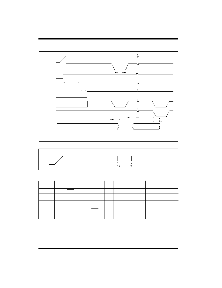
PIC16C72 Series
DS39016A-page 86
Preliminary
©
1998 Microchip Technology Inc.
FIGURE 13-4: RESET, WATCHDOG TIMER, OSCILLATOR START-UP TIMER AND POWER-UP
TIMER TIMING
FIGURE 13-5: BROWN-OUT RESET TIMING
TABLE 13-5
RESET, WATCHDOG TIMER, OSCILLATOR START-UP TIMER, POWER-UP TIMER,
AND BROWN-OUT RESET REQUIREMENTS
Parameter
No.
Sym
Characteristic
Min
Typ
Max
Units
Conditions
30
TmcL
MCLR Pulse Width (low)
2
--
--
µ
s
V
DD
= 5V, -40∞C to +125∞C
31*
Twdt
Watchdog Timer Time-out Period
(No Prescaler)
7
18
33
ms
V
DD
= 5V, -40∞C to +125∞C
32
Tost
Oscillation Start-up Timer Period
--
1024T
OSC
--
--
T
OSC
= OSC1 period
33*
Tpwrt
Power-up Timer Period
28
72
132
ms
V
DD
= 5V, -40∞C to +125∞C
34
T
IOZ
I/O Hi-impedance from MCLR Low
or Watchdog Timer Reset
--
--
2.1
µ
s
35
T
BOR
Brown-out Reset pulse width
100
--
--
µ
s
V
DD
B
VDD
(D005)
*
These parameters are characterized but not tested.
Data in "Typ" column is at 5V, 25∞C unless otherwise stated. These parameters are for design guidance only and are not
tested.
V
DD
MCLR
Internal
POR
PWRT
Time-out
OSC
Time-out
Internal
RESET
Watchdog
Timer
RESET
33
32
30
31
34
I/O Pins
34
Note: Refer to Figure 13-1 for load conditions.
V
DD
BV
DD
35
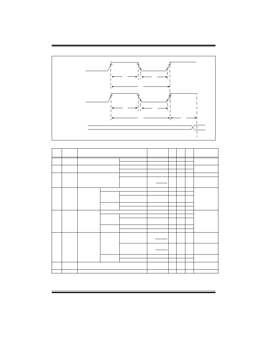
PIC16C72 Series
©
1998 Microchip Technology Inc.
Preliminary
DS39016A-page 87
FIGURE 13-6: TIMER0 AND TIMER1 EXTERNAL CLOCK TIMINGS
TABLE 13-6
TIMER0 AND TIMER1 EXTERNAL CLOCK REQUIREMENTS
Param
No.
Sym
Characteristic
Min
Typ Max Units
Conditions
40*
Tt0H
T0CKI High Pulse Width
No Prescaler
0.5T
CY
+ 20
--
--
ns
Must also meet
parameter 42
With Prescaler
10
--
--
ns
41*
Tt0L
T0CKI Low Pulse Width
No Prescaler
0.5T
CY
+ 20
--
--
ns
Must also meet
parameter 42
With Prescaler
10
--
--
ns
42*
Tt0P
T0CKI Period
No Prescaler
T
CY
+ 40
--
--
ns
With Prescaler
Greater of:
20 or T
CY
+ 40
N
--
--
ns
N = prescale value
(2, 4, ..., 256)
45*
Tt1H
T1CKI High Time Synchronous, Prescaler = 1
0.5T
CY
+ 20
--
--
ns
Must also meet
parameter 47
Synchronous,
Prescaler =
2,4,8
PIC16C7X/CR72
15
--
--
ns
PIC16LC7X/LCR72
25
--
--
ns
Asynchronous PIC16C7X/CR72
30
--
--
ns
PIC16LC7X/LCR72
50
--
--
ns
46*
Tt1L
T1CKI Low Time Synchronous, Prescaler = 1
0.5T
CY
+ 20
--
--
ns
Must also meet
parameter 47
Synchronous,
Prescaler =
2,4,8
PIC16C7X/CR72
15
--
--
ns
PIC16LC7X/LCR72
25
--
--
ns
Asynchronous PIC16C7X/CR72
30
--
--
ns
PIC16LC7X/LCR72
50
--
--
ns
47*
Tt1P
T1CKI input
period
Synchronous
PIC16C7X/CR72
Greater of:
30
OR
T
CY
+ 40
N
--
--
ns
N = prescale value
(1, 2, 4, 8)
PIC16LC7X/LCR72
Greater of:
50
OR
T
CY
+ 40
N
N = prescale value
(1, 2, 4, 8)
Asynchronous PIC16C7X/CR72
60
--
--
ns
PIC16LC7X/LCR72
100
--
--
ns
Ft1
Timer1 oscillator input frequency range
(oscillator enabled by setting bit T1OSCEN)
DC
--
200
kHz
48
TCKEZtmr1 Delay from external clock edge to timer increment
2Tosc
--
7Tosc
--
*
These parameters are characterized but not tested.
Data in "Typ" column is at 5V, 25∞C unless otherwise stated. These parameters are for design guidance only and are not
tested.
Note: Refer to Figure 13-1 for load conditions.
46
47
45
48
41
42
40
RA4/T0CKI
RC0/T1OSO/T1CKI
TMR0 or
TMR1
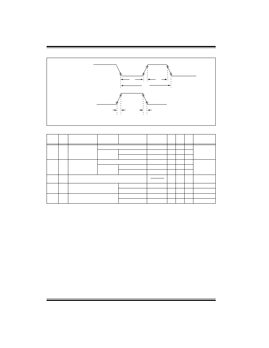
PIC16C72 Series
DS39016A-page 88
Preliminary
©
1998 Microchip Technology Inc.
FIGURE 13-7: CAPTURE/COMPARE/PWM TIMINGS (CCP1)
TABLE 13-7
CAPTURE/COMPARE/PWM REQUIREMENTS (CCP1)
Param
No.
Sym
Characteristic
Min
Typ Max Units
Conditions
50*
TccL
CCP1 input low time
No Prescaler
0.5T
CY
+ 20
--
--
ns
With Prescaler PIC16C72/CR72
10
--
--
ns
PIC16LC72/LCR72
20
--
--
ns
51*
TccH
CCP1 input high time No Prescaler
0.5T
CY
+ 20
--
--
ns
With Prescaler PIC16C72/CR72
10
--
--
ns
PIC16LC72/LCR72
20
--
--
ns
52*
TccP
CCP1 input period
3T
CY
+ 40
N
--
--
ns
N = prescale
value (1,4 or 16)
53*
TccR
CCP1 output rise time
PIC16C72/CR72
--
10
25
ns
PIC16LC72/LCR72
--
25
45
ns
54*
TccF
CCP1 output fall time
PIC16C72/CR72
--
10
25
ns
PIC16LC72/LCR72
--
25
45
ns
*
These parameters are characterized but not tested.
Data in "Typ" column is at 5V, 25∞C unless otherwise stated. These parameters are for design guidance only and are not
tested.
Note: Refer to Figure 13-1 for load conditions.
RC2/CCP1
(Capture Mode)
50
51
52
53
54
RC2/CCP1
(Compare or PWM Mode)
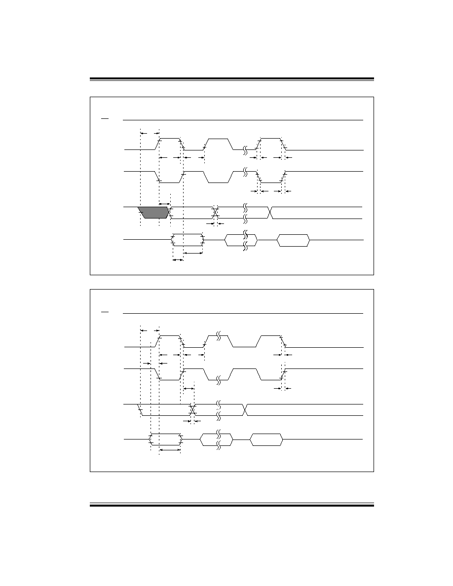
PIC16C72 Series
©
1998 Microchip Technology Inc.
Preliminary
DS39016A-page 89
FIGURE 13-8: SPI MASTER OPERATION TIMING (CKE = 0)
FIGURE 13-9: SPI MASTER OPERATION TIMING (CKE = 1)
SS
SCK
(CKP = 0)
SCK
(CKP = 1)
SDO
SDI
70
71
72
73
74
75, 76
78
79
80
79
78
MSB
LSB
BIT6 - - - - - -1
MSB IN
LSB IN
BIT6 - - - -1
Refer to Figure 13-1 for load conditions.
SS
SCK
(CKP = 0)
SCK
(CKP = 1)
SDO
SDI
81
71
72
74
75, 76
78
80
MSB
79
73
MSB IN
BIT6 - - - - - -1
LSB IN
BIT6 - - - -1
LSB
Refer to Figure 13-1 for load conditions.
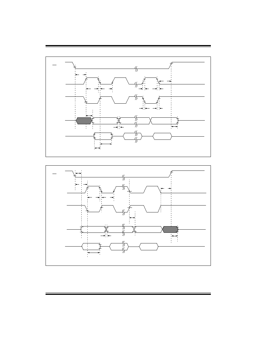
PIC16C72 Series
DS39016A-page 90
Preliminary
©
1998 Microchip Technology Inc.
FIGURE 13-10: SPI SLAVE MODE TIMING (CKE = 0)
FIGURE 13-11: SPI SLAVE MODE TIMING (CKE = 1)
SS
SCK
(CKP = 0)
SCK
(CKP = 1)
SDO
SDI
70
71
72
73
74
75, 76
77
78
79
80
79
78
SDI
MSB
LSB
BIT6 - - - - - -1
MSB IN
BIT6 - - - -1
LSB IN
83
Refer to Figure 13-1 for load conditions.
SS
SCK
(CKP = 0)
SCK
(CKP = 1)
SDO
SDI
70
71
72
82
SDI
74
75, 76
MSB
BIT6 - - - - - -1
LSB
77
MSB IN
BIT6 - - - -1
LSB IN
80
83
Refer to Figure 13-1 for load conditions.
PIC16C72 Series
©
1998 Microchip Technology Inc.
Preliminary
DS39016A-page 91
TABLE 13-8
SPI SLAVE MODE REQUIREMENTS (CKE=0) - PIC16C72
TABLE 13-9
SPI MODE REQUIREMENTS - PIC16CR72
Param
No.
Sym
Characteristic
Min
Typ
Max
Units
Conditions
70
TssL2scH,
TssL2scL
SS
to SCK
or SCK
input
T
CY
--
--
ns
71
TscH
SCK input high time (slave mode)
T
CY
+ 20
--
--
ns
72
TscL
SCK input low time (slave mode)
T
CY
+ 20
--
--
ns
73
TdiV2scH,
TdiV2scL
Setup time of SDI data input to SCK edge
50
--
--
ns
74
TscH2diL,
TscL2diL
Hold time of SDI data input to SCK edge
50
--
--
ns
75
TdoR
SDO data output rise time
--
10
25
ns
76
TdoF
SDO data output fall time
--
10
25
ns
77
TssH2doZ
SS
to SDO output hi-impedance
10
--
50
ns
78
TscR
SCK output rise time (master mode)
--
10
25
ns
79
TscF
SCK output fall time (master mode)
--
10
25
ns
80
TscH2doV,
TscL2doV
SDO data output valid after SCK edge
--
--
50
ns
Data in "Typ" column is at 5V, 25∞C unless otherwise stated. These parameters are for design guidance only and are not
tested.
Parameter
No.
Sym
Characteristic
Min
Typ
Max
Units
Conditions
70*
TssL2scH,
TssL2scL
SS
to SCK
or SCK
input
T
CY
--
--
ns
71*
TscH
SCK input high time (slave mode)
T
CY
+ 20
--
--
ns
72*
TscL
SCK input low time (slave mode)
T
CY
+ 20
--
--
ns
73*
TdiV2scH,
TdiV2scL
Setup time of SDI data input to SCK
edge
100
--
--
ns
74*
TscH2diL,
TscL2diL
Hold time of SDI data input to SCK
edge
100
--
--
ns
75*
TdoR
SDO data output rise time
--
10
25
ns
76*
TdoF
SDO data output fall time
--
10
25
ns
77*
TssH2doZ
SS
to SDO output hi-impedance
10
--
50
ns
78*
TscR
SCK output rise time (master mode)
--
10
25
ns
79*
TscF
SCK output fall time (master mode)
--
10
25
ns
80*
TscH2doV,
TscL2doV
SDO data output valid after SCK
edge
--
--
50
ns
81*
TdoV2scH,
TdoV2scL
SDO data output setup to SCK
edge
T
CY
--
--
ns
82*
TssL2doV
SDO data output valid after SS
edge
--
--
50
ns
83*
TscH2ssH,
TscL2ssH
SS
after SCK edge
1.5T
CY
+ 40
--
--
ns
*
These parameters are characterized but not tested.
Data in "Typ" column is at 5V, 25∞C unless otherwise stated. These parameters are for design guidance only and are not
tested.
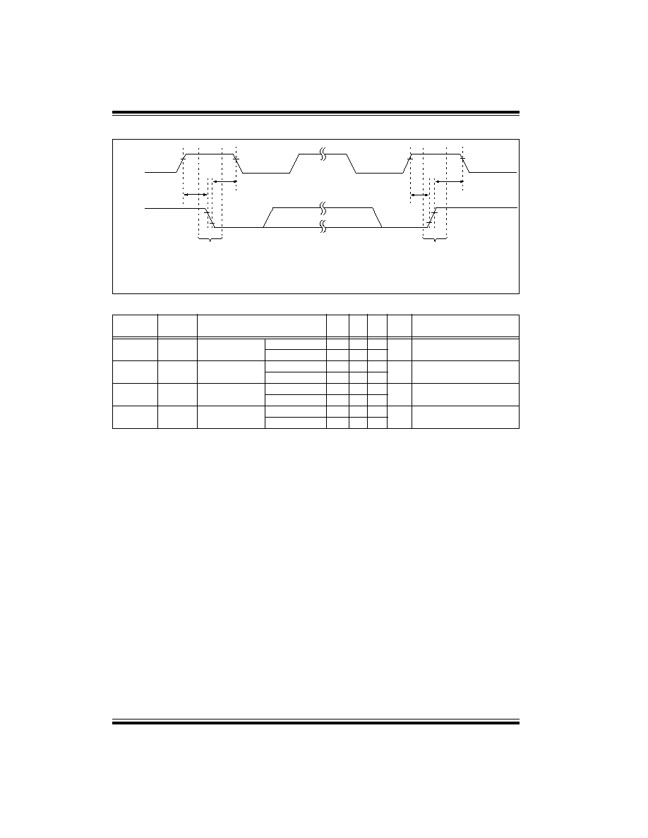
PIC16C72 Series
DS39016A-page 92
Preliminary
©
1998 Microchip Technology Inc.
FIGURE 13-12: I
2
C BUS START/STOP BITS TIMING
TABLE 13-10
I
2
C BUS START/STOP BITS REQUIREMENTS
Parameter
No.
Sym
Characteristic
Min
Typ
Max
Units
Conditions
90
T
SU
:
STA
START condition
100 kHz mode
4700
--
--
ns
Only relevant for repeated START
condition
Setup time
400 kHz mode
600
--
--
91
T
HD
:
STA
START condition
100 kHz mode
4000
--
--
ns
After this period the first clock
pulse is generated
Hold time
400 kHz mode
600
--
--
92
T
SU
:
STO
STOP condition
100 kHz mode
4700
--
--
ns
Setup time
400 kHz mode
600
--
--
93
T
HD
:
STO
STOP condition
100 kHz mode
4000
--
--
ns
Hold time
400 kHz mode
600
--
--
Note: Refer to Figure 13-1 for load conditions
91
93
SCL
SDA
START
Condition
STOP
Condition
90
92
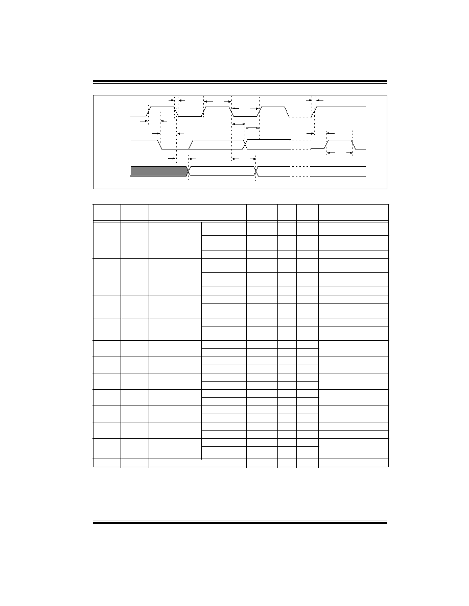
PIC16C72 Series
©
1998 Microchip Technology Inc.
Preliminary
DS39016A-page 93
FIGURE 13-13: I
2
C BUS DATA TIMING
TABLE 13-11
I
2
C BUS DATA REQUIREMENTS
Parameter
No.
Sym
Characteristic
Min
Max
Units
Conditions
100
T
HIGH
Clock high time
100 kHz mode
4.0
--
µ
s
Device must operate at a mini-
mum of 1.5 MHz
400 kHz mode
0.6
--
µ
s
Device must operate at a mini-
mum of 10 MHz
SSP Module
1.5T
CY
--
101
T
LOW
Clock low time
100 kHz mode
4.7
--
µ
s
Device must operate at a mini-
mum of 1.5 MHz
400 kHz mode
1.3
--
µ
s
Device must operate at a mini-
mum of 10 MHz
SSP Module
1.5T
CY
--
102
T
R
SDA and SCL rise
time
100 kHz mode
--
1000
ns
400 kHz mode
20 + 0.1Cb
300
ns
Cb is specified to be from
10 to 400 pF
103
T
F
SDA and SCL fall time 100 kHz mode
--
300
ns
400 kHz mode
20 + 0.1Cb
300
ns
Cb is specified to be from
10 to 400 pF
90
T
SU
:
STA
START condition
setup time
100 kHz mode
4.7
--
µ
s
Only relevant for repeated
START condition
400 kHz mode
0.6
--
µ
s
91
T
HD
:
STA
START condition hold
time
100 kHz mode
4.0
--
µ
s
After this period the first clock
pulse is generated
400 kHz mode
0.6
--
µ
s
106
T
HD
:
DAT
Data input hold time
100 kHz mode
0
--
ns
400 kHz mode
0
0.9
µ
s
107
T
SU
:
DAT
Data input setup time
100 kHz mode
250
--
ns
Note 2
400 kHz mode
100
--
ns
92
T
SU
:
STO
STOP condition setup
time
100 kHz mode
4.7
--
µ
s
400 kHz mode
0.6
--
µ
s
109
T
AA
Output valid from
clock
100 kHz mode
--
3500
ns
Note 1
400 kHz mode
--
--
ns
110
T
BUF
Bus free time
100 kHz mode
4.7
--
µ
s
Time the bus must be free
before a new transmission can
start
400 kHz mode
1.3
--
µ
s
Cb
Bus capacitive loading
--
400
pF
Note 1:
As a transmitter, the device must provide this internal minimum delay time to bridge the undefined region (min. 300 ns) of
the falling edge of SCL to avoid unintended generation of START or STOP conditions.
Note 2:
A fast-mode (400 kHz) I
2
C-bus device can be used in a standard-mode (100 kHz)S I
2
C-bus system, but the requirement
tsu;DAT
250 ns must then be met. This will automatically be the case if the device does not stretch the LOW period of the
SCL signal. If such a device does stretch the LOW period of the SCL signal, it must output the next data bit to the SDA line
T
R
max.+tsu;DAT = 1000 + 250 = 1250 ns (according to the standard-mode I
2
C bus specification) before the SCL line is
released.
Note: Refer to Figure 13-1 for load conditions
90
91
92
100
101
103
106
107
109
109
110
102
SCL
SDA
In
SDA
Out
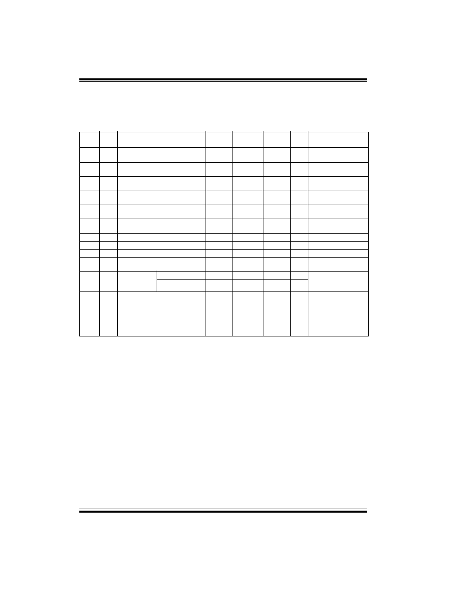
PIC16C72 Series
DS39016A-page 94
Preliminary
©
1998 Microchip Technology Inc.
TABLE 13-12
A/D CONVERTER CHARACTERISTICS:
PIC16C72/CR72-04 (Commercial, Industrial, Extended)
PIC16C72/CR72-10 (Commercial, Industrial, Extended)
PIC16C72/CR72-20 (Commercial, Industrial, Extended)
PIC16LC72/LCR72-04 (Commercial, Industrial)
Param
No.
Sym
Characteristic
Min
Typ
Max
Units
Conditions
A01
N
R
Resolution
--
--
8 bits
bit
V
REF
= V
DD
= 5.12V,
V
SS
V
AIN
V
REF
A02
E
ABS
Total Absolute error
--
--
<
±
1
LSb
V
REF
= V
DD
= 5.12V,
V
SS
V
AIN
V
REF
A03
E
IL
Integral linearity error
--
--
<
±
1
LSb
V
REF
= V
DD
= 5.12V,
V
SS
V
AIN
V
REF
A04
E
DL
Differential linearity error
--
--
<
±
1
LSb
V
REF
= V
DD
= 5.12V,
V
SS
V
AIN
V
REF
A05
E
FS
Full scale error
--
--
<
±
1
LSb
V
REF
= V
DD
= 5.12V,
V
SS
V
AIN
V
REF
A06
E
OFF
Offset error
--
--
<
±
1
LSb
V
REF
= V
DD
= 5.12V,
V
SS
V
AIN
V
REF
A10
--
Monotonicity
--
guaranteed
--
--
V
SS
V
AIN
V
REF
A20
V
REF
Reference voltage
2.5V
--
V
DD
+ 0.3
V
A25
V
AIN
Analog input voltage
V
SS
- 0.3
--
V
REF
+ 0.3
V
A30
Z
AIN
Recommended impedance of
analog voltage source
--
--
10.0
k
A40
I
AD
A/D conversion
current (V
DD
)
PIC16C72/CR72
--
180
--
µ
A
Average current con-
sumption when A/D is
on. (Note 1)
PIC16LC72/LCR72
--
90
--
µ
A
A50
I
REF
V
REF
input current (Note 2)
10
--
--
--
1000
10
µ
A
µ
A
During V
AIN
acquisition.
Based on differential of
V
HOLD
to V
AIN
to charge
C
HOLD
, see Section 9.1.
During A/D Conversion
cycle
*
These parameters are characterized but not tested.
Data in "Typ" column is at 5V, 25
∞
C unless otherwise stated. These parameters are for design guidance only and are not
tested.
Note 1:
When A/D is off, it will not consume any current other than minor leakage current.
The power-down current spec includes any such leakage from the A/D module.
Note 2:
V
REF
current is from RA3 pin or V
DD
pin, whichever is selected as reference input.
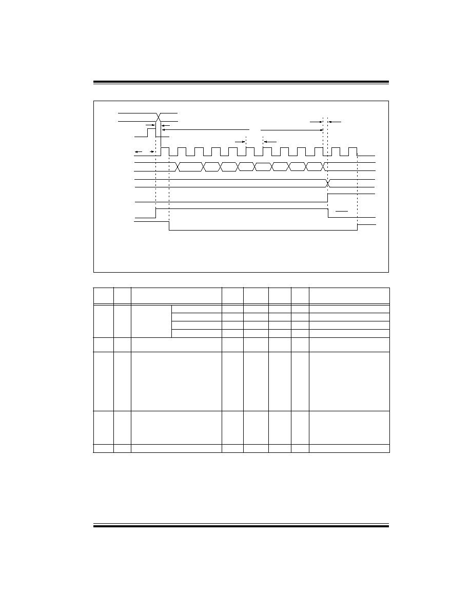
PIC16C72 Series
©
1998 Microchip Technology Inc.
Preliminary
DS39016A-page 95
FIGURE 13-14: A/D CONVERSION TIMING
TABLE 13-13
A/D CONVERSION REQUIREMENTS
Param
No.
Sym
Characteristic
Min
Typ
Max
Units
Conditions
130
T
AD
A/D clock period PIC16C72/LCR72
1.6
--
--
µ
s
T
OSC
based, V
REF
2.5V
PIC16LC72/LCR72
2.0
--
--
µ
s
T
OSC
based, V
REF
full range
PIC16C72/LCR72
2.0
4.0
6.0
µ
s
A/D RC Mode
PIC16LC72/LCR72
2.5
6.0
9.0
µ
s
A/D RC Mode
131
T
CNV
Conversion time
(not including S/H time) (Note 1)
--
9.5
--
T
AD
132
T
ACQ
Acquisition time
Note 2
5*
20
--
--
--
µ
s
µ
s
The minimum time is the amplifier
settling time. This may be used if
the "new" input voltage has not
changed by more than 1 LSb (i.e.,
20.0 mV @ 5.12V) from the last
sampled voltage (as stated on
C
HOLD
).
134
Tgo
Q4 to A/D clock start
--
T
OSC
/2 ß
--
--
If the A/D clock source is selected
as RC, a time of T
CY
is added
before the A/D clock starts. This
allows the
SLEEP
instruction to be
executed.
135
Tswc
Switching from convert
sample time
1.5 ß
--
--
T
AD
*
These parameters are characterized but not tested.
Data in "Typ" column is at 5V, 25
∞
C unless otherwise stated. These parameters are for design guidance only and are not
tested.
ß
This specification ensured by design.
Note 1:
ADRES register may be read on the following T
CY
cycle.
Note 2:
See Section 9.1 for min conditions.
131
130
132
BSF ADCON0, GO
Q4
A/D CLK
A/D DATA
ADRES
ADIF
GO
SAMPLE
OLD_DATA
SAMPLING STOPPED
DONE
NEW_DATA
(T
OSC
/2)
(1)
7
6
5
4
3
2
1
0
Note 1:
If the A/D clock source is selected as RC, a time of T
CY
is added before the A/D clock starts. This allows the
SLEEP
instruction to be executed.
1 T
CY
134

PIC16C72 Series
DS39016A-page 96
Preliminary
©
1998 Microchip Technology Inc.
NOTES:
PIC16C72
PIC16C72 Series
©
1998 Microchip Technology Inc.
Preliminary
DS39016A-page 97
14.0
DC AND AC CHARACTERISTICS GRAPHS AND TABLES - PIC16C72
The graphs and tables provided in this section are for design guidance and are not tested or guaranteed.
In some graphs or tables, the data presented are outside specified operating range (i.e., outside specified V
DD
range). This is for information only and devices are guaranteed to operate properly only within the specified range.
The data presented in this section is a statistical summary of data collected on units from different lots over a period
of time and matrix samples. 'Typical' represents the mean of the distribution at 25
∞
C, while 'max' or 'min' represents
(mean + 3
) and (mean - 3
) respectively, where
is standard deviation.
FIGURE 14-1: TYPICAL I
PD
vs. V
DD
(WDT DISABLED, RC MODE)
FIGURE 14-2: MAXIMUM I
PD
vs. V
DD
(WDT DISABLED, RC MODE)
35
30
25
20
15
10
5
0
2.5
3.0
3.5
4.0
4.5
5.0
5.5
6.0
I
PD
(nA)
V
DD
(Volts)
I
PD
(
µ
A)
V
DD
(Volts)
10.000
1.000
0.100
0.010
0.001
2.5
3.0
3.5
4.0
4.5
5.0
5.5
6.0
85
∞
C
70
∞
C
25
∞
C
0
∞
C
-40
∞
C
PIC16C72 Series
PIC16C72
DS39016A-page 98
Preliminary
©
1998 Microchip Technology Inc.
FIGURE 14-3: TYPICAL I
PD
vs. V
DD
@ 25
∞
C
(WDT ENABLED, RC MODE)
FIGURE 14-4: MAXIMUM I
PD
vs. V
DD
(WDT
ENABLED, RC MODE)
FIGURE 14-5: TYPICAL RC OSCILLATOR
FREQUENCY vs. V
DD
FIGURE 14-6: TYPICAL RC OSCILLATOR
FREQUENCY vs. V
DD
FIGURE 14-7: TYPICAL RC OSCILLATOR
FREQUENCY vs. V
DD
25
20
15
10
5
0
2.5
3.0
3.5
4.0
4.5
5.0
5.5
6.0
I
PD
(
µ
A)
V
DD
(Volts)
35
30
25
20
15
10
5
0
2.5
3.0
3.5
4.0
4.5
5.0
5.5
6.0
I
PD
(
µ
A)
V
DD
(Volts)
-40
∞
C
0
∞
C
70
∞
C
85
∞
C
2.5
3.0
3.5
4.0
4.5
5.0
5.5
6.0
V
DD
(Volts)
6.0
5.5
5.0
4.5
4.0
3.5
3.0
2.5
2.0
1.5
1.0
0.5
0.0
Fosc (MHz)
Cext = 22 pF, T = 25
∞
C
R = 100k
R = 10k
R = 5k
Shaded area is beyond recommended range.
2.5
3.0
3.5
4.0
4.5
5.0
5.5
6.0
V
DD
(Volts)
2.4
2.2
2.0
1.8
1.6
1.4
1.2
1.0
0.8
0.6
0.4
0.2
0.0
Fosc (MHz)
Cext = 100 pF, T = 25
∞
C
R = 100k
R = 10k
R = 5k
R = 3.3k
2.5
3.0
3.5
4.0
4.5
5.0
5.5
6.0
V
DD
(Volts)
1000
900
800
700
600
500
400
300
200
100
0
Fosc (kHz)
Cext = 300 pF, T = 25
∞
C
R = 3.3k
R = 5k
R = 10k
R = 100k
Data based on matr
ix samples
.
See fi
rst page of this section f
or details
.
PIC16C72
PIC16C72 Series
©
1998 Microchip Technology Inc.
Preliminary
DS39016A-page 99
FIGURE 14-8: TYPICAL I
PD
vs. V
DD
BROWN-
OUT DETECT ENABLED (RC
MODE)
FIGURE 14-9: MAXIMUM I
PD
vs. V
DD
BROWN-OUT DETECT
ENABLED
(85
∞
C TO -40
∞
C, RC MODE)
FIGURE 14-10: TYPICAL I
PD
vs. TIMER1
ENABLED (32 kHz, RC0/RC1 =
33 pF/33 pF, RC MODE)
FIGURE 14-11: MAXIMUM I
PD
vs. TIMER1
ENABLED
(32 kHz, RC0/RC1 = 33 pF/33
pF, 85
∞
C TO -40
∞
C, RC MODE)
The shaded region represents the built-in hysteresis of the
brown-out reset circuitry.
2.5
3.0
3.5
4.0
4.5
5.0
5.5
6.0
1400
1200
1000
800
600
400
200
0
V
DD
(Volts)
I
PD
(
µ
A)
Device in
Brown-out
Device NOT in
Brown-out Reset
Reset
The shaded region represents the built-in hysteresis of the
brown-out reset circuitry.
2.5
3.0
3.5
4.0
4.5
5.0
5.5
6.0
1400
1200
1000
800
600
400
200
0
V
DD
(Volts)
I
PD
(
µ
A)
4.3
1600
Device NOT in
Brown-out Reset
Device in
Brown-out
Reset
30
25
20
15
10
5
0
2.5
3.0
3.5
4.0
4.5
5.0
5.5
6.0
V
DD
(Volts)
I
PD
(
µ
A)
30
25
20
15
10
5
0
2.5
3.0
3.5
4.0
4.5
5.0
5.5
6.0
V
DD
(Volts)
I
PD
(
µ
A)
35
40
45
Data based on matr
ix samples
.
See fi
rst page of this section f
or details
.
PIC16C72 Series
PIC16C72
DS39016A-page 100
Preliminary
©
1998 Microchip Technology Inc.
FIGURE 14-12: TYPICAL I
DD
vs. FREQUENCY (RC MODE @ 22 pF, 25
∞
C)
FIGURE 14-13: MAXIMUM I
DD
vs. FREQUENCY (RC MODE @ 22 pF, -40
∞
C TO 85
∞
C)
2000
1800
1600
1400
1200
800
1000
600
400
200
0
0.0
0.5
1.0
1.5
2.0
2.5
3.0
3.5
4.0
4.5
Frequency (MHz)
I
DD
(
µ
A)
Shaded area is
6.0V
5.5V
5.0V
4.5V
4.0V
3.5V
3.0V
2.5V
beyond recommended range
2000
1800
1600
1400
1200
800
1000
600
400
200
0
0.0
0.5
1.0
1.5
2.0
2.5
3.0
3.5
4.0
4.5
Frequency (MHz)
I
DD
(
µ
A)
Shaded area is
6.0V
5.5V
5.0V
4.5V
4.0V
3.5V
3.0V
2.5V
beyond recommended range
Data based on matr
ix samples
.
See fi
rst page of this section f
or details
.
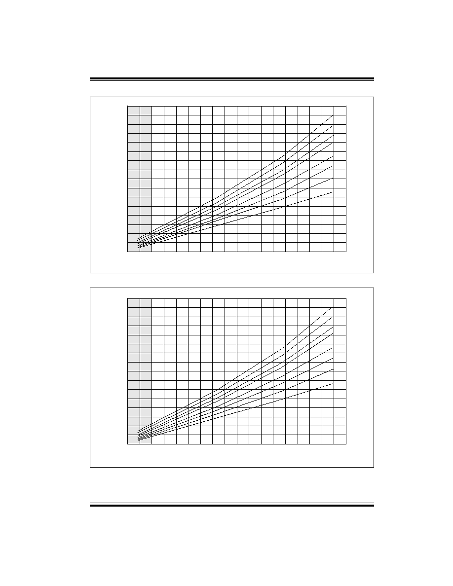
PIC16C72
PIC16C72 Series
©
1998 Microchip Technology Inc.
Preliminary
DS39016A-page 101
FIGURE 14-14: TYPICAL I
DD
vs. FREQUENCY (RC MODE @ 100 pF, 25
∞
C)
FIGURE 14-15: MAXIMUM I
DD
vs. FREQUENCY (RC MODE @ 100 pF, -40
∞
C TO 85
∞
C)
1600
1400
1200
1000
800
600
400
200
0
0
200
400
600
800
1000
1200
1400
1600
1800
Frequency (kHz)
I
DD
(
µ
A)
6.0V
5.5V
5.0V
4.5V
4.0V
3.5V
3.0V
2.5V
Shaded area is
beyond recommended range
1600
1400
1200
1000
800
600
400
200
0
0
200
400
600
800
1000
1200
1400
1600
1800
Frequency (kHz)
I
DD
(
µ
A)
6.0V
5.5V
5.0V
4.5V
4.0V
3.5V
3.0V
2.5V
Shaded area is
beyond recommended range
Data based on matr
ix samples
.
See fi
rst page of this section f
or details
.
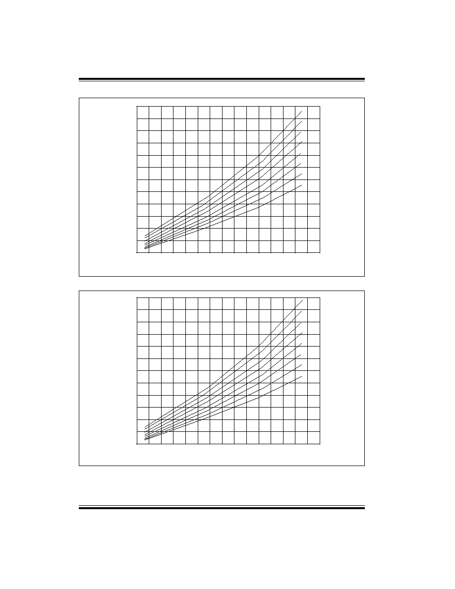
PIC16C72 Series
PIC16C72
DS39016A-page 102
Preliminary
©
1998 Microchip Technology Inc.
FIGURE 14-16: TYPICAL I
DD
vs. FREQUENCY (RC MODE @ 300 pF, 25
∞
C)
FIGURE 14-17: MAXIMUM I
DD
vs. FREQUENCY (RC MODE @ 300 pF, -40
∞
C TO 85
∞
C)
1200
1000
800
600
400
200
0
0
100
200
300
400
500
600
700
Frequency (kHz)
I
DD
(
µ
A)
6.0V
5.5V
5.0V
4.5V
4.0V
3.5V
3.0V
2.5V
1200
1000
800
600
400
200
0
0
100
200
300
400
500
600
700
Frequency (kHz)
I
DD
(
µ
A)
6.0V
5.5V
5.0V
4.5V
4.0V
3.5V
3.0V
2.5V
Data based on matr
ix samples
.
See fi
rst page of this section f
or details
.
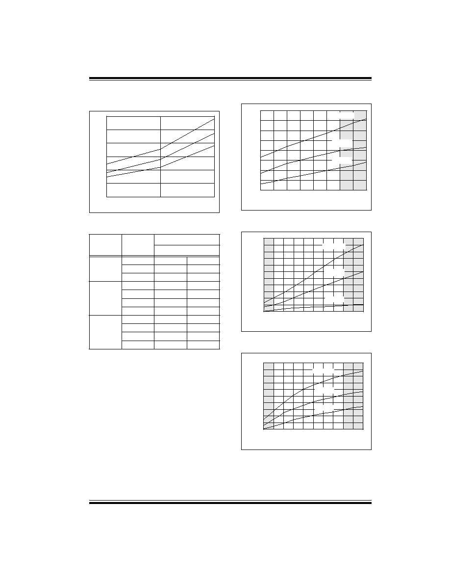
PIC16C72
PIC16C72 Series
©
1998 Microchip Technology Inc.
Preliminary
DS39016A-page 103
FIGURE 14-18: TYPICAL I
DD
vs.
CAPACITANCE @ 500 kHz
(RC MODE)
TABLE 14-1
RC OSCILLATOR
FREQUENCIES
FIGURE 14-19: TRANSCONDUCTANCE(gm)
OF HS OSCILLATOR vs. V
DD
FIGURE 14-20: TRANSCONDUCTANCE(gm)
OF LP OSCILLATOR vs. V
DD
FIGURE 14-21: TRANSCONDUCTANCE(gm)
OF XT OSCILLATOR vs. V
DD
Cext
Rext
Average
Fosc @ 5V, 25
∞
C
22 pF
5k
4.12 MHz
±
1.4%
10k
2.35 MHz
±
1.4%
100k
268 kHz
±
1.1%
100 pF
3.3k
1.80 MHz
±
1.0%
5k
1.27 MHz
±
1.0%
10k
688 kHz
±
1.2%
100k
77.2 kHz
±
1.0%
300 pF
3.3k
707 kHz
±
1.4%
5k
501 kHz
±
1.2%
10k
269 kHz
±
1.6%
100k
28.3 kHz
±
1.1%
The percentage variation indicated here is part to
part variation due to normal process distribution. The
variation indicated is
±
3 standard deviation from
average value for V
DD
= 5V.
Capacitance (pF)
600
I
DD
(
µ
A)
500
400
300
200
100
0
20 pF
100 pF
300 pF
5.0V
4.0V
3.0V
4.0
3.0
3.5
4.0
4.5
5.0
5.5
6.0
6.5
7.0
gm (
m
A/V)
V
DD
(Volts)
3.5
3.0
2.5
2.0
1.5
1.0
0.5
0.0
Max -40
∞
C
Typ 25
∞
C
Min 85
∞
C
Shaded area is
beyond recommended range
110
100
90
80
70
60
50
40
30
20
10
0
2.0
2.5
3.0
3.5
4.0
4.5
5.0
5.5
6.0
6.5
7.0
gm (
µ
A/V)
V
DD
(Volts)
Max -40
∞
C
Typ 25
∞
C
Min 85
∞
C
Shaded areas are
beyond recommended range
1000
900
800
700
600
500
400
300
200
100
0
2.0
2.5
3.0
3.5
4.0
4.5
5.0
5.5
6.0
6.5
7.0
gm (
µ
A/V)
V
DD
(Volts)
Max -40
∞
C
Typ 25
∞
C
Min 85
∞
C
Shaded areas are
beyond recommended range
Data based on matr
ix samples
.
See fi
rst page of this section f
or details
.
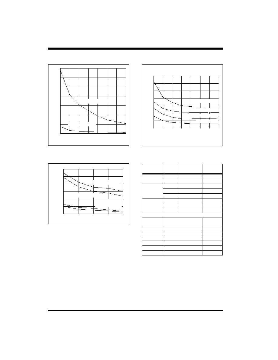
PIC16C72 Series
PIC16C72
DS39016A-page 104
Preliminary
©
1998 Microchip Technology Inc.
FIGURE 14-22: TYPICAL XTAL STARTUP
TIME vs. V
DD
(LP MODE, 25
∞
C)
FIGURE 14-23: TYPICAL XTAL STARTUP
TIME vs. V
DD
(HS MODE,
25
∞
C)
FIGURE 14-24: TYPICAL XTAL STARTUP
TIME vs. V
DD
(XT MODE, 25
∞
C)
TABLE 14-2
CAPACITOR SELECTION
FOR CRYSTAL
OSCILLATORS
3.5
3.0
2.5
2.0
1.5
1.0
0.5
0.0
2.5
3.0
3.5
4.0
4.5
5.0
5.5
6.0
V
DD
(Volts)
Star
tup
Time (Seconds)
32 kHz, 33 pF/33 pF
200 kHz, 15 pF/15 pF
7
6
5
4
3
2
1
4.0
4.5
5.0
5.5
6.0
V
DD
(Volts)
Star
tup
Time (ms)
20 MHz, 33 pF/33 pF
8 MHz, 33 pF/33 pF
8 MHz, 15 pF/15 pF
20 MHz, 15 pF/15 pF
Osc Type
Crystal
Freq
Cap. Range
C1
Cap. Range
C2
LP
32 kHz
33 pF
33 pF
200 kHz
15 pF
15 pF
XT
200 kHz
47-68 pF
47-68 pF
1 MHz
15 pF
15 pF
4 MHz
15 pF
15 pF
HS
4 MHz
15 pF
15 pF
8 MHz
15-33 pF
15-33 pF
20 MHz
15-33 pF
15-33 pF
Crystals
Used
32 kHz
Epson C-001R32.768K-A
±
20 PPM
200 kHz
STD XTL 200.000KHz
±
20 PPM
1 MHz
ECS ECS-10-13-1
±
50 PPM
4 MHz
ECS ECS-40-20-1
±
50 PPM
8 MHz
EPSON CA-301 8.000M-C
±
30 PPM
20 MHz
EPSON CA-301 20.000M-C
±
30 PPM
70
60
50
40
30
20
10
0
3.0
3.5
2.5
4.0
5.0
5.5
6.0
4.5
V
DD
(Volts)
Star
tup
Time (ms)
200 kHz, 68 pF/68 pF
200 kHz, 47 pF/47 pF
1 MHz, 15 pF/15 pF
4 MHz, 15 pF/15 pF
Data based on matr
ix samples
.
See fi
rst page of this section f
or details
.
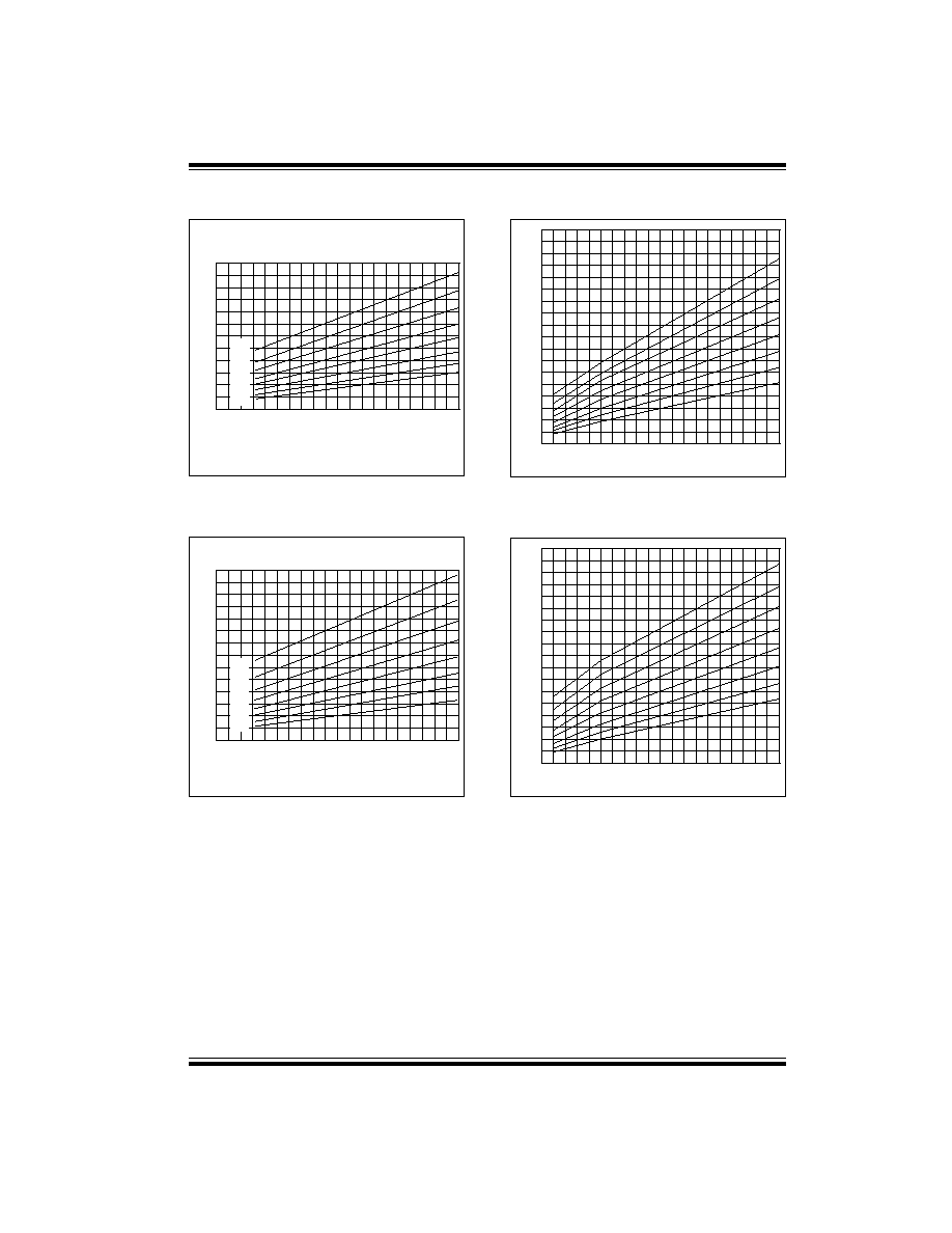
PIC16C72
PIC16C72 Series
©
1998 Microchip Technology Inc.
Preliminary
DS39016A-page 105
FIGURE 14-25: TYPICAL I
DD
vs. FREQUENCY
(LP MODE, 25
∞
C)
FIGURE 14-26: MAXIMUM I
DD
vs.
FREQUENCY
(LP MODE, 85
∞
C TO -40
∞
C)
FIGURE 14-27: TYPICAL I
DD
vs. FREQUENCY
(XT MODE, 25
∞
C)
FIGURE 14-28: MAXIMUM I
DD
vs.
FREQUENCY
(XT MODE, -40
∞
C TO 85
∞
C)
120
100
80
60
40
20
0
0
50
100
150
200
Frequency (kHz)
I
DD
(
µ
A)
6.0V
5.5V
5.0V
4.5V
4.0V
3.5V
3.0V
2.5V
120
100
80
60
40
20
0
0
50
100
150
200
Frequency (kHz)
I
DD
(
µ
A)
140
6.0V
5.5V
5.0V
4.5V
4.0V
3.5V
3.0V
2.5V
1200
1000
800
600
400
200
0
0.0
0.4
Frequency (MHz)
I
DD
(
µ
A)
1400
1600
1800
0.8
1.2
1.6
2.0
2.4
2.8
3.2
3.6
4.0
6.0V
5.5V
5.0V
4.5V
4.0V
3.5V
3.0V
2.5V
1200
1000
800
600
400
200
0
0.0
0.4
Frequency (MHz)
I
DD
(
µ
A)
1400
1600
1800
0.8
1.2
1.6
2.0
2.4
2.8
3.2
3.6
4.0
6.0V
5.5V
5.0V
4.5V
4.0V
3.5V
3.0V
2.5V
Data based on matr
ix samples
.
See fi
rst page of this section f
or details
.
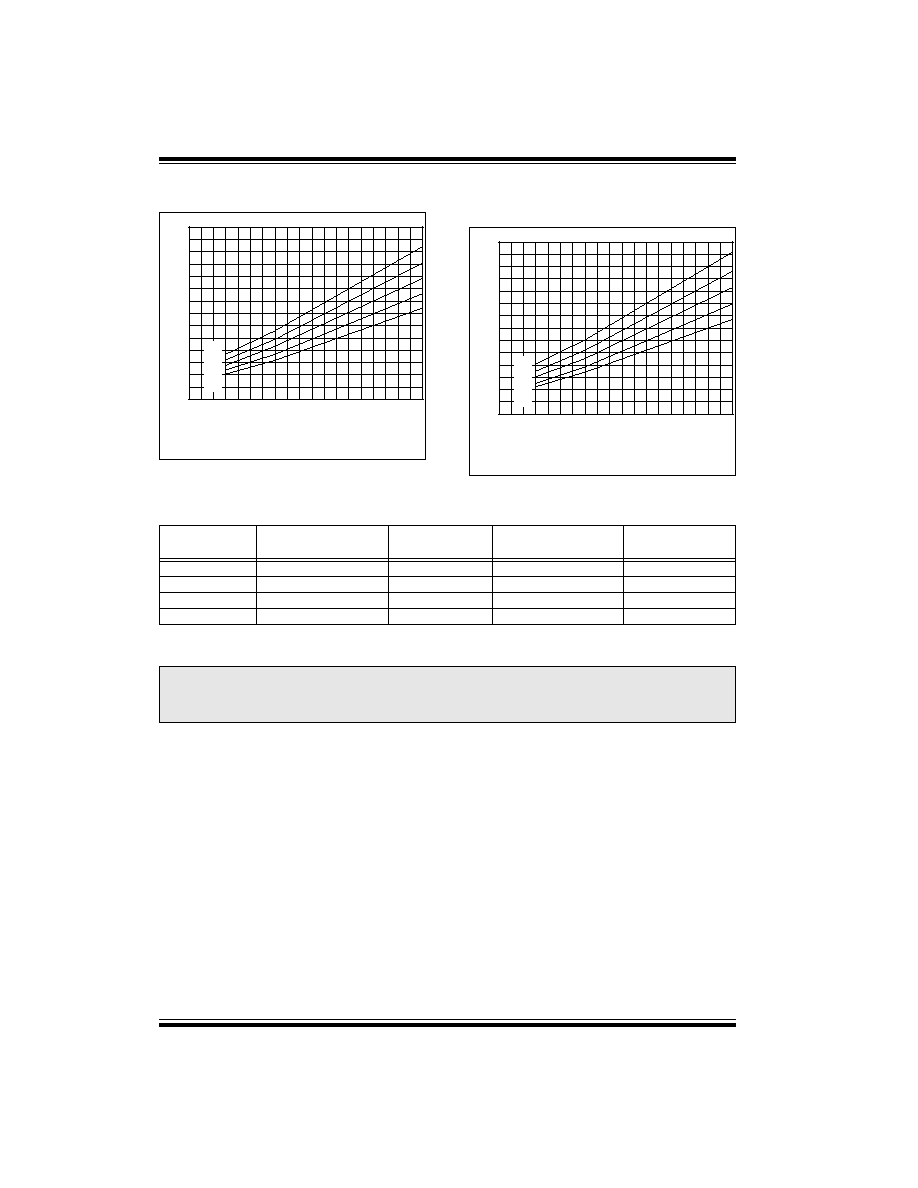
PIC16C72 Series
PIC16C72
DS39016A-page 106
Preliminary
©
1998 Microchip Technology Inc.
FIGURE 14-29: TYPICAL I
DD
vs. FREQUENCY
(HS MODE, 25
∞
C)
FIGURE 14-30: MAXIMUM I
DD
vs.
FREQUENCY
(HS MODE, -40
∞
C TO 85
∞
C)
TABLE 14-3
TYPICAL EPROM ERASE TIME RECOMMENDATIONS
7.0
6.0
5.0
4.0
3.0
2.0
1.0
0.0
1
2
4
6
8
10
12
14
16
18
20
Frequency (MHz)
I
DD
(mA)
6.0V
5.5V
5.0V
4.5V
4.0V
7.0
6.0
5.0
4.0
3.0
2.0
1.0
0.0
1
2
4
6
8
10
12
14
16
18
20
Frequency (MHz)
I
DD
(mA)
6.0V
5.5V
5.0V
4.5V
4.0V
Process
Technology
Wavelength
(Angstroms)
Intensity (
µ
W/
cm2)
Distance from UV lamp
(inches)
Typical Time
(1)
(minutes)
57K
2537
12,000
1
15 - 20
77K
2537
12,000
1
20
90K
2537
12,000
1
40
120K
2537
12,000
1
60
Note 1: If these criteria are not met, the erase times will be different.
Note:
Fluorescent lights and sunlight both emit ultraviolet light at the erasure wavelength. Leaving a UV erasable
device's window uncovered could cause, over time, the devices memory cells to become erased. The era-
sure time for a fluorescent light is about three years. While sunlight requires only about one week. To pre-
vent the memory cells from losing data an opaque label should be placed over the erasure window.
Data based on matr
ix samples
.
See fi
rst page of this section f
or details
.

PIC16CR72
PIC16C72 Series
©
1998 Microchip Technology Inc.
Preliminary
DS39016A-page 107
15.0
DC AND AC CHARACTERISTICS GRAPHS AND TABLES - PIC16CR72
NO GRAPHS OR TABLES AVAILABLE AT THIS TIME

PIC16C72 Series
PIC16CR72
DS39016A-page 108
Preliminary
©
1998 Microchip Technology Inc.
NOTES:
PIC16C72 Series
©
1998 Microchip Technology Inc.
Preliminary
DS39016A-page 109
16.0
PACKAGING INFORMATION
16.1
Package Marking Information
In the event the full Microchip part number cannot be marked on one
line, it will be carried over to the next line thus limiting the number of
available characters for customer specific information.
Note:
Standard OTP marking consists of Microchip part number, year code, week code,
facility code, mask revision number, and assembly code. For OTP marking beyond
this, certain price adders apply. Please check with your Microchip Sales Office.
For QTP devices, any special marking adders are included in QTP price.
*
AABBCAE
XXXXXXXXXXXX
XXXXXXXXXXXX
28-Lead SSOP
9517SBP
20I/SS025
PIC16C72
Example
28-Lead SOIC
XXXXXXXXXXXXXXXXXXXX
AABBCDE
MMMMMMMMMMMMMMMM
Example
945/CAA
PIC16C72-04/SO
XXXXXXXXXXXXXXX
AABBCDE
28-Lead PDIP (Skinny DIP)
MMMMMMMMMMMM
AABBCDE
Example
PIC16C72-04/SP
Example
28-Lead Side Brazed Skinny Windowed
XXXXXXXXXXX
XXXXXXXXXXX
AABBCDE
PIC16C72/JW
9517CAT
Legend: MM...M
Microchip part number information
XX...X
Customer specific information*
AA
Year code (last 2 digits of calendar year)
BB
Week code (week of January 1 is week `01')
C
Facility code of the plant at which wafer is manufactured
O = Outside Vendor
C = 5" Line
S = 6" Line
H = 8" Line
D
Mask revision number
E
Assembly code of the plant or country of origin in which
part was assembled
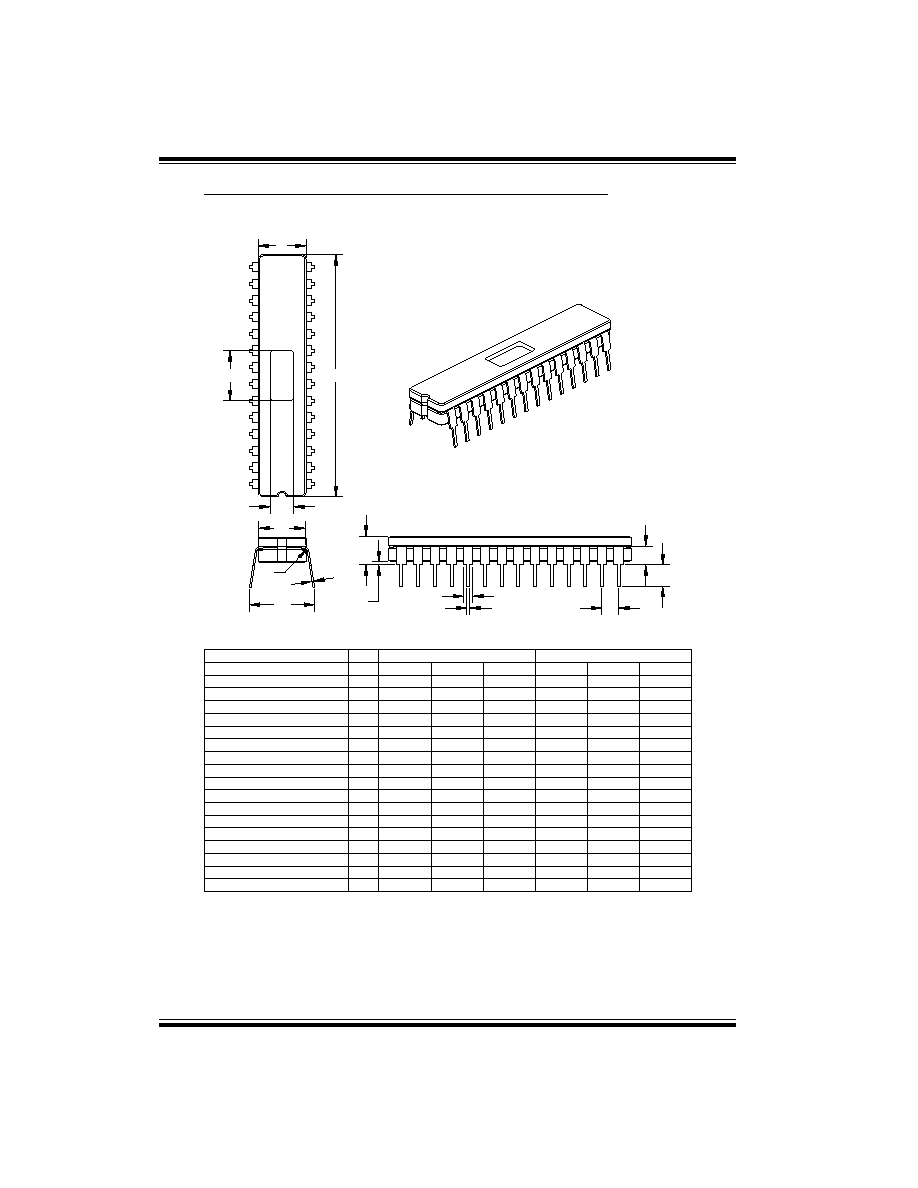
PIC16C72 Series
DS39016A-page 110
Preliminary
©
1998 Microchip Technology Inc.
16.2
28-Lead Ceramic Side Brazed Dual In-Line with Window (300 mil)(JW)
*
Controlling Parameter.
n
1
2
R
Overall Row Spacing
Radius to Radius Width
Package Length
Tip to Seating Plane
Base to Seating Plane
Top of Lead to Seating Plane
Top to Seating Plane
Shoulder Radius
Upper Lead Width
Lower Lead Width
PCB Row Spacing
Dimension Limits
Window Width
Window Length
Package Width
Lead Thickness
Pitch
Number of Pins
Units
0.170
A
0.130
W1
W2
0.290
D
E1
eB
E
A2
L
A1
1.430
0.345
0.255
0.285
0.135
0.015
0.107
B
R
c
B1
n
p
0.016
0.008
0.010
0.050
0.098
MIN
MILLIMETERS
4.32
0.195
0.183
0.310
0.150
0.425
0.285
0.295
1.485
0.145
0.030
0.143
0.140
0.300
0.385
0.270
0.290
1.458
0.140
0.023
0.125
0.13
0.29
36.32
8.76
6.48
7.24
3.43
0.00
2.72
0.012
0.015
0.065
0.021
0.102
MAX
NOM
0.010
0.013
0.058
0.019
0.100
0.300
28
INCHES*
0.41
0.20
0.25
1.27
2.49
MIN
4.95
4.64
0.31
0.15
10.80
7.24
7.49
37.72
3.68
0.76
3.63
0.14
0.3
37.02
6.86
9.78
7.37
0.57
3.56
3.18
0.30
0.38
1.65
0.53
2.59
NOM
28
0.47
0.32
0.25
1.46
2.54
7.62
MAX
D
W2
W1
E
c
E1
eB
p
A1
L
B1
B
A2
A
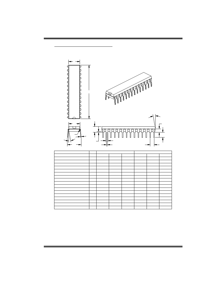
PIC16C72 Series
©
1998 Microchip Technology Inc.
Preliminary
DS39016A-page 111
16.3
28-Lead Plastic Dual In-line (300 mil) (SP)
*
Controlling Parameter.
Dimension "B1" does not include dam-bar protrusions. Dam-bar protrusions shall not exceed 0.003"
(0.076 mm) per side or 0.006" (0.152 mm) more than dimension "B1."
Dimensions "D" and "E" do not include mold flash or protrusions. Mold flash or protrusions shall not
exceed 0.010" (0.254 mm) per side or 0.020" (0.508 mm) more than dimensions "D" or "E."
0.320
0.270
0.280
1.345
0.125
0.015
0.070
0.140
0.008
0.000
0.040
0.016
Mold Draft Angle Bottom
Mold Draft Angle Top
Overall Row Spacing
Radius to Radius Width
Molded Package Width
Tip to Seating Plane
Base to Seating Plane
Top of Lead to Seating Plane
Top to Seating Plane
Upper Lead Width
Lower Lead Width
PCB Row Spacing
Package Length
Lead Thickness
Shoulder Radius
Number of Pins
Dimension Limits
Pitch
Units
E
eB
E1
A1
A2
L
D
A
c
R
n
B1
B
p
MIN
MIN
0.295
0.288
5
5
10
0.350
0.283
10
0.380
0.295
15
15
0.090
1.365
0.130
0.020
0.150
0.010
0.005
NOM
INCHES*
28
0.053
0.019
0.100
0.300
1.385
0.135
0.025
0.110
0.160
0.012
0.010
0.065
0.022
MAX
7.49
7.30
7.11
8.89
7.18
5
8.13
6.86
5
10
10
15
15
9.65
7.49
34.67
3.30
0.51
2.29
3.81
0.25
0.13
1.33
0.48
2.54
7.62
MILLIMETERS
1.78
34.16
3.18
0.38
3.56
0.20
0.00
1.02
0.41
NOM
2.79
35.18
3.43
0.64
4.06
0.30
0.25
MAX
28
1.65
0.56
n
1
2
R
D
E
c
eB
E1
p
L
A1
B
B1
A
A2
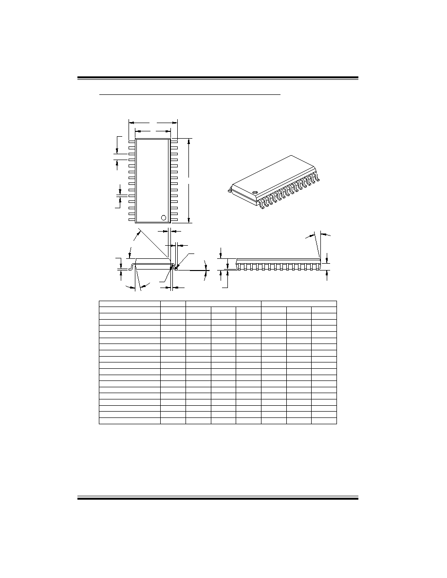
PIC16C72 Series
DS39016A-page 112
Preliminary
©
1998 Microchip Technology Inc.
16.4
28-Lead Plastic Surface Mount (SOIC - Wide, 300 mil Body) (SO)
MIN
p
Pitch
Mold Draft Angle Bottom
Mold Draft Angle Top
Lower Lead Width
Radius Centerline
Gull Wing Radius
Shoulder Radius
Chamfer Distance
Outside Dimension
Molded Package Width
Molded Package Length
Shoulder Height
Overall Pack. Height
Lead Thickness
Foot Angle
Foot Length
Standoff
Number of Pins
B
c
X
A2
A1
A
n
E1
L
L1
R1
R2
E
D
Dimension Limits
Units
1.27
0.050
8
12
12
0.017
0
0.014
0
0.019
15
15
0.011
0.015
0.016
0.005
0.005
0.020
0.407
0.296
0.706
0.008
0.058
0.099
28
0.394
0.011
0.009
0.010
0
0.005
0.005
0.010
0.292
0.700
0.004
0.048
0.093
0.419
0.012
0.020
0.021
0.010
0.010
0.029
4
8
0.299
0.712
0.011
0.068
0.104
0.36
0
0
12
12
0.42
15
15
0.48
10.33
17.93
10.01
0.23
0.25
0.28
0.13
0.13
0.25
0
7.42
0.10
1.22
2.36
17.78
10.64
0.41
4
0.27
0.38
0.13
0.13
0.50
0.53
0.30
0.51
0.25
0.25
0.74
7.51
0.19
28
2.50
1.47
18.08
7.59
0.28
2.64
1.73
NOM
INCHES*
MAX
NOM
MILLIMETERS
MIN
MAX
n
1
2
R1
R2
D
p
B
E1
E
L1
L
c
45
∞
X
A1
A
A2
*
Controlling Parameter.
Dimension "B" does not include dam-bar protrusions. Dam-bar protrusions shall not exceed 0.003"
(0.076 mm) per side or 0.006" (0.152 mm) more than dimension "B."
Dimensions "D" and "E" do not include mold flash or protrusions. Mold flash or protrusions shall not
exceed 0.010" (0.254 mm) per side or 0.020" (0.508 mm) more than dimensions "D" or "E."
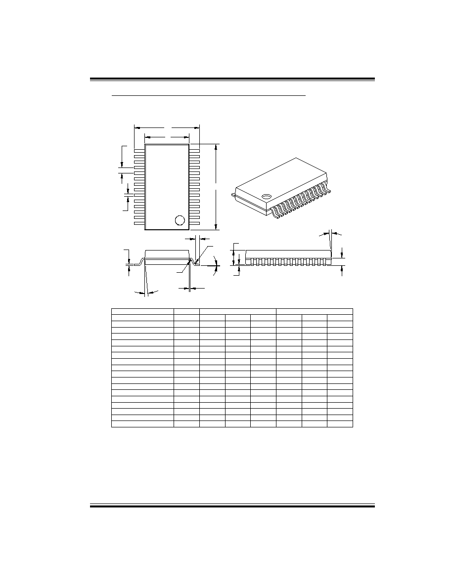
PIC16C72 Series
©
1998 Microchip Technology Inc.
Preliminary
DS39016A-page 113
16.5
28-Lead Plastic Surface Mount (SSOP - 209 mil Body 5.30 mm) (SS)
Dimension Limits
Mold Draft Angle Bottom
Mold Draft Angle Top
Lower Lead Width
Lead Thickness
Radius Centerline
Gull Wing Radius
Shoulder Radius
Outside Dimension
Molded Package Width
Molded Package Length
Shoulder Height
Overall Pack. Height
Number of Pins
Foot Angle
Foot Length
Standoff
Pitch
B
E
L
c
L1
R1
R2
E1
A2
D
A1
A
n
p
Units
MAX
NOM
MIN
MAX
NOM
MIN
10
10
0.38
0.22
0.25
0.64
0.25
0.25
7.90
5.38
10.33
0.21
1.17
1.99
0.012
0
0.010
0
5
5
10
0.015
10
0.007
0.005
0.020
0.005
0.005
0.306
0.208
0.402
0.005
0.036
0.073
0.026
0.205
0.015
0.005
0.000
0
0.005
0.005
0.301
0.396
0.002
0.026
0.068
0.212
4
0.025
0.009
0.010
8
0.010
0.010
0.311
28
0.407
0.008
0.046
0.078
0.25
0
0
5
0.32
5
5.20
0.13
0.00
0.38
0.13
0.13
7.65
0
10.07
0.05
0.66
1.73
5.29
0.51
0.18
0.13
4
0.13
0.13
7.78
10.20
0.13
0.91
1.86
0.65
28
8
INCHES
MILLIMETERS*
n
1
2
R1
R2
D
p
B
E
E1
L
L1
c
A1
A2
A
*
Controlling Parameter.
Dimension "B" does not include dam-bar protrusions. Dam-bar protrusions shall not exceed 0.003"
(0.076 mm) per side or 0.006" (0.152 mm) more than dimension "B."
Dimensions "D" and "E" do not include mold flash or protrusions. Mold flash or protrusions shall not
exceed 0.010" (0.254 mm) per side or 0.020" (0.508 mm) more than dimensions "D" or "E."

PIC16C72 Series
DS39016A-page 114
Preliminary
©
1998 Microchip Technology Inc.
NOTES:

PIC16C72 Series
©
1998 Microchip Technology Inc.
Preliminary
DS39016A-page 115
APPENDIX A: WHAT'S NEW IN THIS
DATA SHEET
This is a new data sheet. However, information on the
PIC16C72 device was previously found in the
PIC16C7X Data Sheet, DS30390. Information on the
PIC16CR72 device is new.
APPENDIX B: WHAT'S CHANGED IN
THIS DATA SHEET
New data sheet.
APPENDIX C: DEVICE DIFFERENCES
A table of the differences between the devices
described in this document is found below.
Difference
PIC16C72
PIC16CR72
SSP module in
SPI mode
Basic SSP
SSP

PIC16C72 Series
DS39016A-page 116
Preliminary
©
1998 Microchip Technology Inc.
NOTES:

PIC16C72 Series
©
1998 Microchip Technology Inc.
Preliminary
DS39016A-page 117
INDEX
A
A/D
ADCON0 Register ...................................................... 53
ADCON1 Register ...................................................... 54
ADIF bit ...................................................................... 55
Analog Input Model Block Diagram ............................ 56
Analog-to-Digital Converter ........................................ 53
Block Diagram ............................................................ 55
Configuring Analog Port Pins ..................................... 57
Configuring the Interrupt ............................................ 55
Configuring the Module .............................................. 55
Conversion Clock ....................................................... 57
Conversions ............................................................... 58
Converter Characteristics .......................................... 94
GO/DONE bit ............................................................. 55
Internal Sampling Switch (Rss) Impedance ............... 56
Sampling Requirements ............................................. 56
Source Impedance ..................................................... 56
Using the CCP Trigger ............................................... 58
Absolute Maximum Ratings ............................................... 77
ACK .............................................................................. 47, 49
ADIE bit .............................................................................. 12
ADIF bit .............................................................................. 13
ADRES Register ...................................................... 7, 53, 55
Application Notes
AN546 (Using the Analog-to-Digital Converter) ......... 53
AN578 (Use of the SSP Module in the I
2
C
Multi-Master Environment) ......................................... 39
B
BF .......................................................................... 40, 43, 47
Block Diagrams
A/D ............................................................................. 55
Analog Input Model .................................................... 56
Capture ...................................................................... 34
Compare .................................................................... 35
I
2
C Mode .................................................................... 47
On-Chip Reset Circuit ................................................ 62
PIC16C72 .................................................................... 3
PIC16CR72 .................................................................. 3
PORTC ...................................................................... 23
PWM .......................................................................... 36
RA3:RA0 and RA5 Port Pins ..................................... 19
RA4/T0CKI Pin ........................................................... 19
RB3:RB0 Port Pins .................................................... 21
RB7:RB4 Port Pins .................................................... 21
SSP in I
2
C Mode ........................................................ 47
SSP in SPI Mode ................................................. 42, 45
Timer0 ........................................................................ 25
Timer0/WDT Prescaler .............................................. 26
Timer2 ........................................................................ 31
Watchdog Timer ......................................................... 70
BOR bit ........................................................................ 14, 64
Buffer Full Status bit, BF .............................................. 40, 43
C
C bit ...................................................................................... 9
Capture/Compare/PWM
Capture
Block Diagram ................................................... 34
CCP1CON Register ........................................... 33
CCP1IF .............................................................. 34
CCPR1 ............................................................... 34
CCPR1H:CCPR1L ............................................. 34
Mode ................................................................. 34
Prescaler ........................................................... 34
CCP Timer Resources ............................................... 33
Compare
Block Diagram ................................................... 35
Mode ................................................................. 35
Software Interrupt Mode .................................... 35
Special Event Trigger ........................................ 35
Special Trigger Output of CCP1 ........................ 35
Special Trigger Output of CCP2 ........................ 35
Section ....................................................................... 33
Special Event Trigger and A/D Conversions ............. 35
Capture/Compare/PWM (CCP)
PWM Block Diagram ................................................. 36
PWM Mode ................................................................ 36
PWM, Example Frequencies/Resolutions ................. 37
CCP1IE bit ......................................................................... 12
CCP1IF bit ......................................................................... 13
CCPR1H Register ............................................................. 33
CCPR1L Register .............................................................. 33
CCPxM0 bit ....................................................................... 33
CCPxM1 bit ....................................................................... 33
CCPxM2 bit ....................................................................... 33
CCPxM3 bit ....................................................................... 33
CCPxX bit .......................................................................... 33
CCPxY bit .......................................................................... 33
CKE ................................................................................... 43
CKP ............................................................................. 41, 44
Clock Polarity Select bit, CKP ..................................... 41, 44
Code Examples
Changing Between Capture Prescalers .................... 34
Initializing PORTA ..................................................... 19
Initializing PORTB ..................................................... 21
Initializing PORTC ..................................................... 23
Code Protection ........................................................... 59, 72
Configuration Bits .............................................................. 59
D
D/A ............................................................................... 40, 43
Data/Address bit, D/A .................................................. 40, 43
DC bit ....................................................................................9
DC Characteristics
PIC16C72 .................................................................. 79
Development Support ........................................................ 75
Development Tools ............................................................ 75
Direct Addressing .............................................................. 17
E
Electrical Characteristics
PIC16C72 .................................................................. 77
External Power-on Reset Circuit ....................................... 63
F
FSR Register ............................................................. 7, 8, 17
Fuzzy Logic Dev. System (
fuzzy
TECH
Æ
-MP) ................... 75
G
GIE bit ................................................................................ 68
I
I/O Ports
PORTA ...................................................................... 19
PORTB ...................................................................... 21
PORTC ...................................................................... 23
Section ....................................................................... 19
I
2
C
Addressing ................................................................. 48

PIC16C72 Series
DS39016A-page 118
Preliminary
©
1998 Microchip Technology Inc.
Block Diagram ............................................................ 47
I
2
C Operation ............................................................. 47
Master Mode .............................................................. 51
Mode .......................................................................... 47
Mode Selection .......................................................... 47
Multi-Master Mode ..................................................... 51
Reception ................................................................... 49
Reception Timing Diagram ........................................ 49
SCL and SDA pins ..................................................... 47
Slave Mode ................................................................ 47
Transmission .............................................................. 50
In-Circuit Serial Programming ...................................... 59, 72
INDF Register ................................................................ 8, 17
Indirect Addressing ............................................................ 17
Initialization Condition for all Register ................................ 65
Instruction Format .............................................................. 73
Instruction Set
Section ....................................................................... 73
Summary Table .......................................................... 74
INT Interrupt ....................................................................... 68
INTCON Register ............................................................... 11
INTEDG bit ................................................................... 10, 68
Internal Sampling Switch (Rss) Impedance ....................... 56
Interrupts ............................................................................ 59
PortB Change ............................................................ 68
RB7:RB4 Port Change ............................................... 21
Section ....................................................................... 68
TMR0 ......................................................................... 68
IRP bit .................................................................................. 9
L
Loading of PC .................................................................... 15
M
MCLR ........................................................................... 61, 64
Memory
Data Memory ............................................................... 6
Program Memory ......................................................... 5
Program Memory Maps
PIC16C72 ............................................................ 5
PIC16CR72 .......................................................... 5
Register File Maps
PIC16C72 ............................................................ 6
PIC16CR72 .......................................................... 6
MPASM Assembler ............................................................ 75
MPSIM Software Simulator ................................................ 75
O
OPCODE ............................................................................ 73
OPTION Register ............................................................... 10
OSC selection .................................................................... 59
Oscillator
HS ........................................................................ 60, 64
LP ......................................................................... 60, 64
RC .............................................................................. 60
XT ........................................................................ 60, 64
Oscillator Configurations .................................................... 60
Output of TMR2 .................................................................. 31
P
P ................................................................................... 40, 43
Packaging
28-Lead Ceramic w/Window .................................... 110
28-Lead PDIP .......................................................... 111
28-Lead SOIC .......................................................... 112
28-Lead SSOP ......................................................... 113
Paging, Program Memory .................................................. 16
PCFG0 bit .......................................................................... 54
PCFG1 bit .......................................................................... 54
PCFG2 bit .......................................................................... 54
PCL Register ............................................................. 7, 8, 15
PCLATH ............................................................................. 65
PCLATH Register ...................................................... 7, 8, 15
PCON Register ............................................................ 14, 64
PD bit ............................................................................. 9, 61
PICDEM-1 Low-Cost PIC16/17 Demo Board .................... 75
PICDEM-2 Low-Cost PIC16CXX Demo Board .................. 75
PICMASTER
TM
RT In-Circuit Emulator .............................. 75
PICSTART
TM
Low-Cost Development System ................... 75
PIE1 Register ..................................................................... 12
Pin Functions
MCLR/Vpp ................................................................... 4
OSC1/CLKIN ............................................................... 4
OSC2/CLKOUT ........................................................... 4
RA0/AN0 ...................................................................... 4
RA1/AN1 ...................................................................... 4
RA2/AN2 ...................................................................... 4
RA3/AN3/Vref .............................................................. 4
RA4/T0CKI .................................................................. 4
RA5/AN4/SS ................................................................ 4
RB0/INT ....................................................................... 4
RB1 .............................................................................. 4
RB2 .............................................................................. 4
RB3 .............................................................................. 4
RB4 .............................................................................. 4
RB5 .............................................................................. 4
RB6 .............................................................................. 4
RB7 .............................................................................. 4
RC0/T1OSO/T1CKI ..................................................... 4
RC1/T1OSI .................................................................. 4
RC2/CCP1 ................................................................... 4
RC3/SCK/SCL ............................................................. 4
RC4/SDI/SDA .............................................................. 4
RC5/SDO ..................................................................... 4
RC6 ............................................................................. 4
RC7 ............................................................................. 4
SCK ..................................................................... 42≠??
SDI ....................................................................... 42≠??
SDO ..................................................................... 42≠??
SS ........................................................................ 42≠??
Vdd .............................................................................. 4
Vss ............................................................................... 4
Pinout Descriptions
PIC16C72 .................................................................... 4
PIC16CR72 ................................................................. 4
PIR1 Register .................................................................... 13
POR ............................................................................. 63, 64
Oscillator Start-up Timer (OST) ........................... 59, 63
Power Control Register (PCON) ................................ 64
Power-on Reset (POR) ........................................ 59, 65
Power-up Timer (PWRT) ........................................... 59
Power-Up-Timer (PWRT) .......................................... 63
Time-out Sequence ................................................... 64
TO .............................................................................. 61
POR bit ........................................................................ 14, 64
Port RB Interrupt ................................................................ 68
PORTA .............................................................................. 65
PORTA Register ............................................................ 7, 19
PORTB .............................................................................. 65
PORTB Register ............................................................ 7, 21
PORTC .............................................................................. 65
PORTC Register ............................................................ 7, 23
Power-down Mode (SLEEP) .............................................. 71

PIC16C72 Series
©
1998 Microchip Technology Inc.
Preliminary
DS39016A-page 119
PR2 Register ...................................................................... 31
Prescaler, Switching Between Timer0 and WDT ............... 26
PRO MATE
TM
Universal Programmer ................................ 75
Program Memory
Paging ........................................................................ 16
Program Memory Maps
PIC16C72 .................................................................... 5
PIC16CR72 .................................................................. 5
Program Verification .......................................................... 72
PS0 bit ............................................................................... 10
PS1 bit ............................................................................... 10
PS2 bit ............................................................................... 10
PSA bit ............................................................................... 10
R
R/W .............................................................................. 40, 43
R/W bit ................................................................... 48, 49, 50
RBIF bit ........................................................................ 21, 68
RBPU bit ............................................................................ 10
RC Oscillator ................................................................ 61, 64
Read/Write bit Information, R/W .................................. 40, 43
Receive Overflow Detect bit, SSPOV ................................ 41
Receive Overflow Indicator bit, SSPOV ............................. 44
Register File ......................................................................... 6
Registers
Initialization Conditions .............................................. 65
Maps
PIC16C72 ............................................................ 6
PIC16CR72 .......................................................... 6
Reset Conditions ........................................................ 64
SSPCON
Diagram ............................................................. 41
SSPSTAT ................................................................... 43
Diagram ............................................................. 40
Section ............................................................... 40
Reset ............................................................................ 59, 61
Reset Conditions for Special Registers ............................. 64
RP0 bit ............................................................................. 6, 9
RP1 bit ................................................................................. 9
S
S ................................................................................... 40, 43
SCK .................................................................................... 42
SCL .................................................................................... 47
SDI ..................................................................................... 42
SDO ................................................................................... 42
Slave Mode
SCL ............................................................................ 47
SDA ............................................................................ 47
SLEEP ......................................................................... 59, 61
SMP ................................................................................... 43
Special Event Trigger ......................................................... 58
Special Features of the CPU ............................................. 59
Special Function Registers
PIC16C72 .................................................................... 7
PIC16CR72 .................................................................. 7
Special Function Registers, Section .................................... 7
SPI
Block Diagram ...................................................... 42, 45
Mode .......................................................................... 42
Serial Clock ................................................................ 45
Serial Data In ............................................................. 45
Serial Data Out .......................................................... 45
Slave Select ............................................................... 45
SPI Mode ................................................................... 45
SSPCON .................................................................... 44
SSPSTAT ................................................................... 43
SPI Clock Edge Select bit, CKE ........................................ 43
SPI Data Input Sample Phase Select bit, SMP ................. 43
SPI Mode ........................................................................... 42
SS ...................................................................................... 42
SSP
Module Overview ....................................................... 39
Section ....................................................................... 39
SSPCON ................................................................... 44
SSPSTAT .................................................................. 43
SSPADD Register ................................................................8
SSPCON ..................................................................... 41, 44
SSPEN ........................................................................ 41, 44
SSPIE bit ........................................................................... 12
SSPIF bit ........................................................................... 13
SSPM3:SSPM0 ........................................................... 41, 44
SSPOV .................................................................. 41, 44, 47
SSPSTAT .......................................................................... 40
SSPSTAT Register ........................................................ 8, 43
Stack .................................................................................. 16
Start bit, S .................................................................... 40, 43
STATUS Register .................................................................9
Stop bit, P .................................................................... 40, 43
Synchronous Serial Port (SSP)
Block Diagram, SPI Mode ......................................... 42
SPI Mode ................................................................... 42
Synchronous Serial Port Enable bit, SSPEN ............... 41, 44
Synchronous Serial Port Mode Select bits,
SSPM3:SSPM0 ........................................................... 41, 44
Synchronous Serial Port Module ....................................... 39
Synchronous Serial Port Status Register .......................... 43
T
T0CS bit ............................................................................. 10
T1CKPS0 bit ...................................................................... 27
T1CKPS1 bit ...................................................................... 27
T1CON Register ................................................................ 27
T1OSCEN bit ..................................................................... 27
T1SYNC bit ........................................................................ 27
T2CKPS0 bit ...................................................................... 32
T2CKPS1 bit ...................................................................... 32
T2CON Register ................................................................ 32
T
AD
.................................................................................... 57
Timer0
RTCC ......................................................................... 65
Timers
Timer0
Block Diagram ................................................... 25
Interrupt ............................................................. 26
Prescaler ........................................................... 25
Prescaler Block Diagram ................................... 26
Section .............................................................. 25
Switching Prescaler Assignment ....................... 26
T0IF ................................................................... 68
TMR0 Interrupt .................................................. 68
Timer1
Capacitor Selection ........................................... 29
Oscillator ........................................................... 29
Resetting Timer1 using a CCP Trigger Output .. 29
T1CON .............................................................. 27
Timer2
Block Diagram ................................................... 31
Postscaler .......................................................... 31
Prescaler ........................................................... 31
T2CON .............................................................. 32

PIC16C72 Series
DS39016A-page 120
Preliminary
©
1998 Microchip Technology Inc.
Timing Diagrams
A/D Conversion .......................................................... 95
Brown-out Reset ........................................................ 86
Capture/Compare/PWM ............................................. 88
CLKOUT and I/O ........................................................ 85
External Clock Timing ................................................ 84
I
2
C Bus Data .............................................................. 93
I
2
C Bus Start/Stop bits ............................................... 92
I
2
C Reception (7-bit Address) .................................... 49
Power-up Timer ......................................................... 86
Reset .......................................................................... 86
Start-up Timer ............................................................ 86
Timer0 ........................................................................ 87
Timer1 ........................................................................ 87
Wake-up from Sleep via Interrupt .............................. 72
Watchdog Timer ......................................................... 86
TMR1CS bit ........................................................................ 27
TMR1H Register .................................................................. 7
TMR1IE bit ......................................................................... 12
TMR1IF bit ......................................................................... 13
TMR1L Register ................................................................... 7
TMR1ON bit ....................................................................... 27
TMR2 Register ..................................................................... 7
TMR2IE bit ......................................................................... 12
TMR2IF bit ......................................................................... 13
TMR2ON bit ....................................................................... 32
TO bit ................................................................................... 9
TOUTPS0 bit ...................................................................... 32
TOUTPS1 bit ...................................................................... 32
TOUTPS2 bit ...................................................................... 32
TOUTPS3 bit ...................................................................... 32
TRISA Register .............................................................. 8, 19
TRISB Register .............................................................. 8, 21
TRISC Register .............................................................. 8, 23
U
UA ................................................................................ 40, 43
Update Address bit, UA ................................................ 40, 43
W
Wake-up from SLEEP ........................................................ 71
Watchdog Timer (WDT) ................................... 59, 61, 64, 70
WCOL .......................................................................... 41, 44
WDT ................................................................................... 64
Block Diagram ............................................................ 70
Timeout ...................................................................... 65
Write Collision Detect bit, WCOL ................................. 41, 44
Z
Z bit ...................................................................................... 9

©
1998 Microchip Technology Inc.
DS39016A-page 121
PIC16C72 Series
Systems Information and Upgrade Hot Line
The Systems Information and Upgrade Line provides
system users a listing of the latest versions of all of
Microchip's development systems software products.
Plus, this line provides information on how customers
can receive any currently available upgrade kits.The
Hot Line Numbers are:
1-800-755-2345 for U.S. and most of Canada, and
1-602-786-7302 for the rest of the world.
Trademarks: The Microchip name, logo, PIC, PICSTART,
PICMASTER and PRO MATE are registered trademarks
of Microchip Technology Incorporated in the U.S.A. and
other countries. PICmicro,
Flex
ROM, MPLAB and
fuzzy-
LAB are trademarks and SQTP is a service mark of Micro-
chip in the U.S.A.
All other trademarks mentioned herein are the property of
their respective companies.
ON-LINE SUPPORT
Microchip provides on-line support on the Microchip
World Wide Web (WWW) site.
The web site is used by Microchip as a means to make
files and information easily available to customers. To
view the site, the user must have access to the Internet
and a web browser, such as Netscape or Microsoft
Explorer. Files are also available for FTP download
from our FTP site.
Connecting to the Microchip Internet Web Site
The Microchip web site is available by using your
favorite Internet browser to attach to:
www.microchip.com
The file transfer site is available by using an FTP ser-
vice to connect to:
ftp://ftp.futureone.com/pub/microchip
The web site and file transfer site provide a variety of
services. Users may download files for the latest
Development Tools, Data Sheets, Application Notes,
User's Guides, Articles and Sample Programs. A vari-
ety of Microchip specific business information is also
available, including listings of Microchip sales offices,
distributors and factory representatives. Other data
available for consideration is:
∑ Latest Microchip Press Releases
∑ Technical Support Section with Frequently Asked
Questions
∑ Design Tips
∑ Device Errata
∑ Job Postings
∑ Microchip Consultant Program Member Listing
∑ Links to other useful web sites related to
Microchip Products
∑ Conferences for products, Development Systems,
technical information and more
∑ Listing of seminars and events
980106

PIC16C72 Series
DS39016A-page 122
©
1998 Microchip Technology Inc.
READER RESPONSE
It is our intention to provide you with the best documentation possible to ensure successful use of your Microchip prod-
uct. If you wish to provide your comments on organization, clarity, subject matter, and ways in which our documentation
can better serve you, please FAX your comments to the Technical Publications Manager at (602) 786-7578.
Please list the following information, and use this outline to provide us with your comments about this Data Sheet.
1.
What are the best features of this document?
2.
How does this document meet your hardware and software development needs?
3.
Do you find the organization of this data sheet easy to follow? If not, why?
4.
What additions to the data sheet do you think would enhance the structure and subject?
5.
What deletions from the data sheet could be made without affecting the overall usefulness?
6.
Is there any incorrect or misleading information (what and where)?
7.
How would you improve this document?
8.
How would you improve our software, systems, and silicon products?
To:
Technical Publications Manager
RE:
Reader Response
Total Pages Sent
From: Name
Company
Address
City / State / ZIP / Country
Telephone: (_______) _________ - _________
Application (optional):
Would you like a reply? Y N
Device:
Literature Number:
Questions:
FAX: (______) _________ - _________
DS39016A
PIC16C72 Series

PIC16C72 Series
©
1998 Microchip Technology Inc.
Preliminary
DS39016A-page 123
PIC16C72 SERIES PRODUCT IDENTIFICATION SYSTEM
To order or obtain information, e.g., on pricing or delivery, refer to the factory or the listed sales office.
* JW Devices are UV erasable and can be programmed to any device configuration. JW Devices meet the electrical requirement of
each oscillator type (including LC devices).
SALES AND SUPPORT
PART NO.
-XX
X
/XX
XXX
Pattern
Package
Temperature
Range
Frequency
Range
Device
Device
PIC16C72
(1)
, PIC16C72T
(2)
PIC16LC72
(1)
, PIC16LC72T
(2)
PIC16CR72
(1)
, PIC16CR72T
(2)
PIC16LCR72
(1)
, PIC16LCR72T
(2)
Frequency Range
02
= 2 MHz
04
= 4 MHz
10
= 10 MHz
20
= 20 MHz
Temperature Range
b
(3)
=
0
∞
C to
70
∞
C
(Commercial)
I
= -40
∞
C to
+85
∞
C
(Industrial)
E
= -40
∞
C to +125
∞
C
(Extended)
Package
JW
= Ceramic Dual In-Line Package with Window
SO
= Small Outline - 300 mil
SP
= Skinny PDIP
SS
= Shrink Samll Outline Package - 209 mil
Pattern
3-digit Pattern Code for QTP, ROM (blank otherwise)
Examples:
f)
PIC16C72 -04/P 301 = Commercial temp.,
PDIP package, 4 MHz, normal V
DD
limits, QTP
pattern #301.
g)
PIC16LC72 - 04I/SO = Industrial temp., SOIC
package, 200 kHz, Extended V
DD
limits.
h)
PIC16CR72 - 10I/P = ROM program memory,
Industrial temp., PDIP package, 10MHz, nor-
mal V
DD
limits.
Note 1:
C= CMOS
CR= CMOS ROM
LC= Low Power CMOS
LCR= ROM Version, Extended Vdd range
2:
T = in tape and reel - SOIC, SSOP pack-
ages only.
3:
b = blank
Data Sheets
Products supported by a preliminary Data Sheet may have an errata sheet describing minor operational differences and recom-
mended workarounds. To determine if an errata sheet exists for a particular device, please contact one of the following:
1.
Your local Microchip sales office (see last page)
2.
The Microchip Corporate Literature Center U.S. FAX: (602) 786-7277
3.
The Microchip's Bulletin Board, via your local CompuServe number (CompuServe membership NOT required).
Please specify which device, revision of silicon and Data Sheet (include Literature #) you are using.
Development Tools
For the latest version information and upgrade kits for Microchip Development Tools, please call 1-800-755-2345 or 1-602-786-7302.
The latest version of Development Tools software can be downloaded from either our Bulletin Board or Worldwide Web Site. (Infor-
mation on how to connect to our BBS or WWW site can be found in the On-Line Support section of this data sheet.)
Information contained in this publication regarding device applications and the like is intended for suggestion only and may be superseded by updates. No representation or warranty is given and no
liability is assumed by Microchip Technology Incorporated with respect to the accuracy or use of such information, or infringement of patents or other intellectual property rights arising from such use
or otherwise. Use of Microchip's products as critical components in life support systems is not authorized except with express written approval by Microchip. No licenses are conveyed, implicitly or
otherwise, under any intellectual property rights. The Microchip logo and name are registered trademarks of Microchip Technology Inc. in the U.S.A. and other countries. All rights reserved. All other
trademarks mentioned herein are the property of their respective companies.
DS39016A-page 124
©
1998 Microchip Technology Inc.
All rights reserved. © 1998, Microchip Technology Incorporated, USA. 2/98
Printed on recycled paper.
M
AMERICAS
Corporate Office
Microchip Technology Inc.
2355 West Chandler Blvd.
Chandler, AZ 85224-6199
Tel: 602-786-7200 Fax: 602-786-7277
Technical Support: 602 786-7627
Web: http://www.microchip.com
Atlanta
Microchip Technology Inc.
500 Sugar Mill Road, Suite 200B
Atlanta, GA 30350
Tel: 770-640-0034 Fax: 770-640-0307
Boston
Microchip Technology Inc.
5 Mount Royal Avenue
Marlborough, MA 01752
Tel: 508-480-9990 Fax: 508-480-8575
Chicago
Microchip Technology Inc.
333 Pierce Road, Suite 180
Itasca, IL 60143
Tel: 630-285-0071 Fax: 630-285-0075
Dallas
Microchip Technology Inc.
14651 Dallas Parkway, Suite 816
Dallas, TX 75240-8809
Tel: 972-991-7177 Fax: 972-991-8588
Dayton
Microchip Technology Inc.
Two Prestige Place, Suite 150
Miamisburg, OH 45342
Tel: 937-291-1654 Fax: 937-291-9175
Los Angeles
Microchip Technology Inc.
18201 Von Karman, Suite 1090
Irvine, CA 92612
Tel: 714-263-1888 Fax: 714-263-1338
New York
Microchip Technology Inc.
150 Motor Parkway, Suite 202
Hauppauge, NY 11788
Tel: 516-273-5305 Fax: 516-273-5335
San Jose
Microchip Technology Inc.
2107 North First Street, Suite 590
San Jose, CA 95131
Tel: 408-436-7950 Fax: 408-436-7955
Toronto
Microchip Technology Inc.
5925 Airport Road, Suite 200
Mississauga, Ontario L4V 1W1, Canada
Tel: 905-405-6279 Fax: 905-405-6253
ASIA/PACIFIC
Hong Kong
Microchip Asia Pacific
RM 3801B, Tower Two
Metroplaza
223 Hing Fong Road
Kwai Fong, N.T., Hong Kong
Tel: 852-2-401-1200 Fax: 852-2-401-3431
India
Microchip Technology Inc.
India Liaison Office
No. 6, Legacy, Convent Road
Bangalore 560 025, India
Tel: 91-80-229-0061 Fax: 91-80-229-0062
Japan
Microchip Technology Intl. Inc.
Benex S-1 6F
3-18-20, Shinyokohama
Kohoku-Ku, Yokohama-shi
Kanagawa 222 Japan
Tel: 81-45-471- 6166 Fax: 81-45-471-6122
Korea
Microchip Technology Korea
168-1, Youngbo Bldg. 3 Floor
Samsung-Dong, Kangnam-Ku
Seoul, Korea
Tel: 82-2-554-7200 Fax: 82-2-558-5934
Shanghai
Microchip Technology
RM 406 Shanghai Golden Bridge Bldg.
2077 Yan'an Road West, Hong Qiao District
Shanghai, PRC 200335
Tel: 86-21-6275-5700
Fax: 86 21-6275-5060
Singapore
Microchip Technology Taiwan
Singapore Branch
200 Middle Road
#07-02 Prime Centre
Singapore 188980
Tel: 65-334-8870 Fax: 65-334-8850
ASIA/PACIFIC
(CONTINUED)
Taiwan, R.O.C
Microchip Technology Taiwan
10F-1C 207
Tung Hua North Road
Taipei, Taiwan, ROC
Tel: 886-2-2717-7175 Fax: 886-2-2545-0139
EUROPE
United Kingdom
Arizona Microchip Technology Ltd.
505 Eskdale Road
Winnersh Triangle
Wokingham
Berkshire, England RG41 5TU
Tel: 44-1189-21-5858 Fax: 44-1189-21-5835
France
Arizona Microchip Technology SARL
Zone Industrielle de la Bonde
2 Rue du Buisson aux Fraises
91300 Massy, France
Tel: 33-1-69-53-63-20 Fax: 33-1-69-30-90-79
Germany
Arizona Microchip Technology GmbH
Gustav-Heinemann-Ring 125
D-81739 M¸chen, Germany
Tel: 49-89-627-144 0 Fax: 49-89-627-144-44
Italy
Arizona Microchip Technology SRL
Centro Direzionale Colleoni
Palazzo Taurus 1 V. Le Colleoni 1
20041 Agrate Brianza
Milan, Italy
Tel: 39-39-6899939 Fax: 39-39-6899883
1/13/98
W
ORLDWIDE
S
ALES
AND
S
ERVICE
Microchip received ISO 9001 Quality
System certification for its worldwide
headquarters, design, and wafer
fabrication facilities in January, 1997.
Our field-programmable PICmicroTM
8-bit MCUs, Serial EEPROMs,
related specialty memory products
and development systems conform
to the stringent quality standards of
the International Standard
Organization (ISO).