
2002 Microchip Technology Inc.
Preliminary
DS41159B
PIC18FXX8
Data Sheet
High Performance, 28/40-Pin
Enhanced FLASH Microcontrollers
with CAN
M

DS41159B - page ii
Preliminary
2002 Microchip Technology Inc.
Information contained in this publication regarding device
applications and the like is intended through suggestion only
and may be superseded by updates. It is your responsibility to
ensure that your application meets with your specifications.
No representation or warranty is given and no liability is
assumed by Microchip Technology Incorporated with respect
to the accuracy or use of such information, or infringement of
patents or other intellectual property rights arising from such
use or otherwise. Use of Microchip's products as critical com-
ponents in life support systems is not authorized except with
express written approval by Microchip. No licenses are con-
veyed, implicitly or otherwise, under any intellectual property
rights.
Trademarks
The Microchip name and logo, the Microchip logo, FilterLab,
K
EE
L
OQ
, microID, MPLAB, PIC, PICmicro, PICMASTER,
PICSTART, PRO MATE, SEEVAL and The Embedded Control
Solutions Company are registered trademarks of Microchip Tech-
nology Incorporated in the U.S.A. and other countries.
dsPIC, ECONOMONITOR, FanSense, FlexROM, fuzzyLAB,
In-Circuit Serial Programming, ICSP, ICEPIC, microPort,
Migratable Memory, MPASM, MPLIB, MPLINK, MPSIM,
MXDEV, MXLAB, PICC, PICDEM, PICDEM.net, rfPIC, Select
Mode and Total Endurance are trademarks of Microchip
Technology Incorporated in the U.S.A.
Serialized Quick Turn Programming (SQTP) is a service mark
of Microchip Technology Incorporated in the U.S.A.
All other trademarks mentioned herein are property of their
respective companies.
� 2002, Microchip Technology Incorporated, Printed in the
U.S.A., All Rights Reserved.
Printed on recycled paper.
Microchip received QS-9000 quality system
certification for its worldwide headquarters,
design and wafer fabrication facilities in
Chandler and Tempe, Arizona in July 1999
and Mountain View, California in March 2002.
The Company's quality system processes and
procedures are QS-9000 compliant for its
PICmicro
�
8-bit MCUs, K
EE
L
OQ
�
code hopping
devices, Serial EEPROMs, microperipherals,
non-volatile memory and analog products. In
addition, Microchip's quality system for the
design and manufacture of development
systems is ISO 9001 certified.
Note the following details of the code protection feature on PICmicro
�
MCUs.
�
The PICmicro family meets the specifications contained in the Microchip Data Sheet.
�
Microchip believes that its family of PICmicro microcontrollers is one of the most secure products of its kind on the market today,
when used in the intended manner and under normal conditions.
�
There are dishonest and possibly illegal methods used to breach the code protection feature. All of these methods, to our knowl-
edge, require using the PICmicro microcontroller in a manner outside the operating specifications contained in the data sheet.
The person doing so may be engaged in theft of intellectual property.
�
Microchip is willing to work with the customer who is concerned about the integrity of their code.
�
Neither Microchip nor any other semiconductor manufacturer can guarantee the security of their code. Code protection does not
mean that we are guaranteeing the product as "unbreakable".
�
Code protection is constantly evolving. We at Microchip are committed to continuously improving the code protection features of
our product.
If you have any further questions about this matter, please contact the local sales office nearest to you.

2002 Microchip Technology Inc.
Preliminary
DS41159B-page 1
M
PIC18FXX8
High Performance RISC CPU:
� Linear program memory addressing up to
2 Mbytes
� Linear data memory addressing to 4 Kbytes
� Up to 10 MIPs operation
� DC - 40 MHz clock input
� 4 MHz - 10 MHz osc./clock input with PLL active
� 16-bit wide instructions, 8-bit wide data path
� Priority levels for interrupts
� 8 x 8 Single Cycle Hardware Multiplier
Peripheral Features:
� High current sink/source 25 mA/25 mA
� Three external interrupt pins
� Timer0 module: 8-bit/16-bit timer/counter with
8-bit programmable prescaler
� Timer1 module: 16-bit timer/counter
� Timer2 module: 8-bit timer/counter with 8-bit
period register (time-base for PWM)
� Timer3 module: 16-bit timer/counter
� Secondary oscillator clock option - Timer1/Timer3
� Capture/Compare/PWM (CCP) modules CCP
pins can be configured as:
- Capture input: 16-bit, max resolution 6.25 ns
- Compare: 16-bit, max resolution 100 ns (T
CY
)
- PWM output: PWM resolution is 1- to 10-bit
Max. PWM freq. @:8-bit resolution = 156 kHz
10-bit resolution = 39 kHz
� Enhanced CCP module which has all the features
of the standard CCP module, but also has the
following features for advanced motor control:
- 1, 2, or 4 PWM outputs
- Selectable PWM polarity
- Programmable PWM deadtime
� Master Synchronous Serial Port (MSSP) with two
modes of operation:
- 3-wire SPITM (Supports all 4 SPI modes)
- I
2
CTM Master and Slave mode
� Addressable USART module: Supports Interrupt
on Address bit
Advanced Analog Features:
� 10-bit, up to 8-channel Analog-to-Digital Converter
module (A/D) with:
- Conversion available during SLEEP
- Up to 8 channels available
� Analog Comparator Module:
- Programmable input and output multiplexing
� Comparator Voltage Reference Module
� Programmable Low Voltage Detection (LVD) module
- Supports interrupt on low voltage detection
� Programmable Brown-out Reset (BOR)
CAN bus Module Features:
� Message bit rates up to 1 Mbps
� Conforms to CAN 2.0B ACTIVE Spec with:
- 29-bit Identifier Fields
- 8-byte message length
- 3 Transmit Message Buffers with prioritiza-
tion
- 2 Receive Message Buffers
- 6 full 29-bit Acceptance Filters
- Prioritization of Acceptance Filters
- Multiple Receive Buffers for High Priority
Messages to prevent loss due to overflow
- Advanced Error Management Features
Special Microcontroller Features:
� Power-on Reset (POR), Power-up Timer (PWRT),
and Oscillator Start-up Timer (OST)
� Watchdog Timer (WDT) with its own on-chip RC
oscillator
� Programmable code protection
� Power saving SLEEP mode
� Selectable oscillator options, including:
- 4X Phase Lock Loop (of primary oscillator)
- Secondary Oscillator (32 kHz) clock input
� In-Circuit Serial Programming
TM
(ICSP
TM
) via two pins
FLASH Technology:
� Low power, high speed Enhanced FLASH technology
� Fully static design
� Wide operating voltage range (2.0V to 5.5V)
� Industrial and Extended temperature ranges
High Performance, 28/40-Pin Enhanced FLASH
Microcontrollers with CAN
PIC18FXX8
DS41159B-page 2
Preliminary
2002 Microchip Technology Inc.
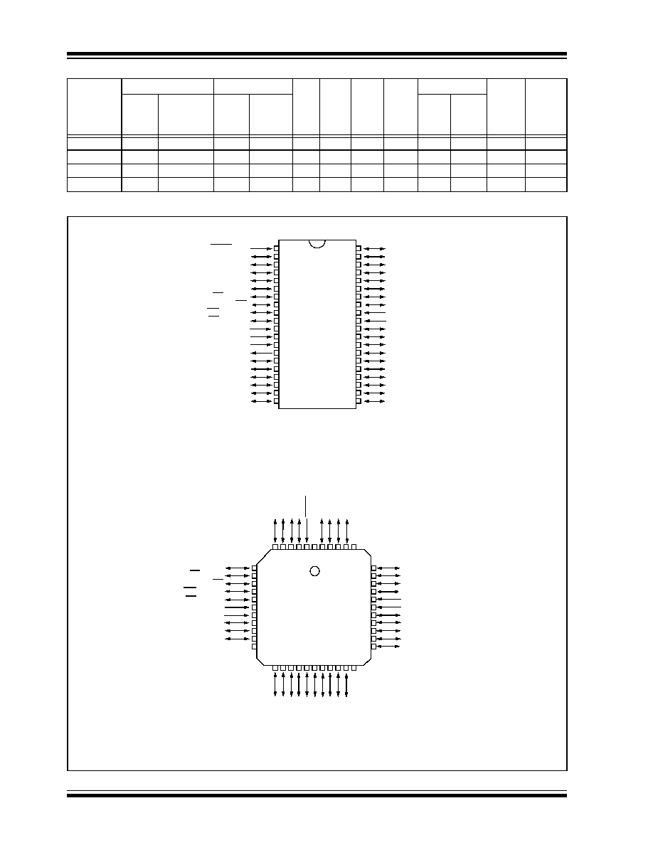
Pin Diagrams
Device
Program Memory
Data Memory
I/O
10-bit
A/D
(ch)
Co
mp
arato
r
s
CCP/
ECCP
(PWM)
MSSP
USART
Timers
8/16-bit
FLASH
(bytes)
# Single
Word
Instructions
SRAM
(bytes)
EEPROM
(bytes)
SPI
Master
I
2
C
PIC18F248
16K
8192
768
256
22
5
--
1/0
Y
Y
Y
1/3
PIC18F258
32K
16384
1536
256
22
5
--
1/0
Y
Y
Y
1/3
PIC18F448
16K
8192
768
256
33
8
2
1/1
Y
Y
Y
1/3
PIC18F458
32K
16384
1536
256
33
8
2
1/1
Y
Y
Y
1/3
RB7/PGD
RB6/PGC
RB5/PGM
RB4
RB3/CANRX
RB2/CANTX/INT2
RB1/INT1
RB0/INT0
V
DD
V
SS
RD7/PSP7/P1D
RD6/PSP6/P1C
RD5/PSP5/P1B
RD4/PSP4/ECCP1/P1A
RC7/RX/DT
RC6/TX/CK
RC5/SDO
RC4/SDI/SDA
RD3/PSP3/C2IN-
RD2/PSP2/C2IN+
MCLR/V
PP
RA0/AN0/C
VREF
RA1/AN1
RA2/AN2/V
REF
-
RA3/AN3/V
REF
+
RA4/T0CKI
RA5/AN4/SS/LVDIN
RE0/AN5/RD
RE1/AN6/WR/C1OUT
RE2/AN7/CS/C2OUT
V
DD
V
SS
OSC1/CLKI
OSC2/CLKO/RA6
RC0/T1OSO/T1CKI
RC1/T1OSI
RC2/CCP1
RC3/SCK/SCL
RD0/PSP0/C1IN+
RD1/PSP1/C1IN-
1
2
3
4
5
6
7
8
9
10
11
12
13
14
15
16
17
18
19
20
40
39
38
37
36
35
34
33
32
31
30
29
28
27
26
25
24
23
22
21
PIC1
8F4
5
8
PDIP
RB3/CANRX
NC
RC6
/T
X/CK
RC5
/SDO
RC4
/SDI/SDA
RD3
/PSP
3
/
C2
I
N
-
RD2
/
PSP2
/
C
2
I
N+
RD1
/PSP
1
/
C1
I
N
-
RD0
/
PSP0
/
C
1
I
N+
RC3
/SCK/SCL
RC2
/
CCP1
1
PIC18F458
PLCC
RC1
/
T
1
O
SI
2
3
4
5
6
7
8
9
10
11
12
13
14
15
16
17
18 19
20
21
22
23
24
25
26
27
28
29
30
31
32
33
34
35
36
37
38
39
40
41
42
43
44
RB2/CANTX/INT2
RB1/INT1
RB0/INT0
V
DD
RD7/PSP7/P1D
V
SS
RD6/PSP6/P1C
RD5/PSP5/P1B
RD4/PSP4/ECCP1/P1A
RC7/RX/DT
RA
3
/
AN3
/
V
RE
F
+
RA
2
/
AN2
/
V
RE
F
-
RA1
/
AN1
RA
0
/
AN0
/
CV
RE
F
MC
LR
/V
PP
NC RB
7
/
PGD
RB
6
/
PGC
RB
5
/
PGM
RB
4
NC
RA4/T0CKI
RA5/AN4/SS/LVDIN
RE0/AN5/RD
RE1/AN6/WR/C1OUT
RE2/AN7/CS/C2OUT
V
DD
V
SS
OSC1/CLKI
OSC2/CLKO/RA6
NC
RC0/T1OSO/T1CK1
PIC1
8F4
4
8
PIC18F448
2002 Microchip Technology Inc.
Preliminary
DS41159B-page 3
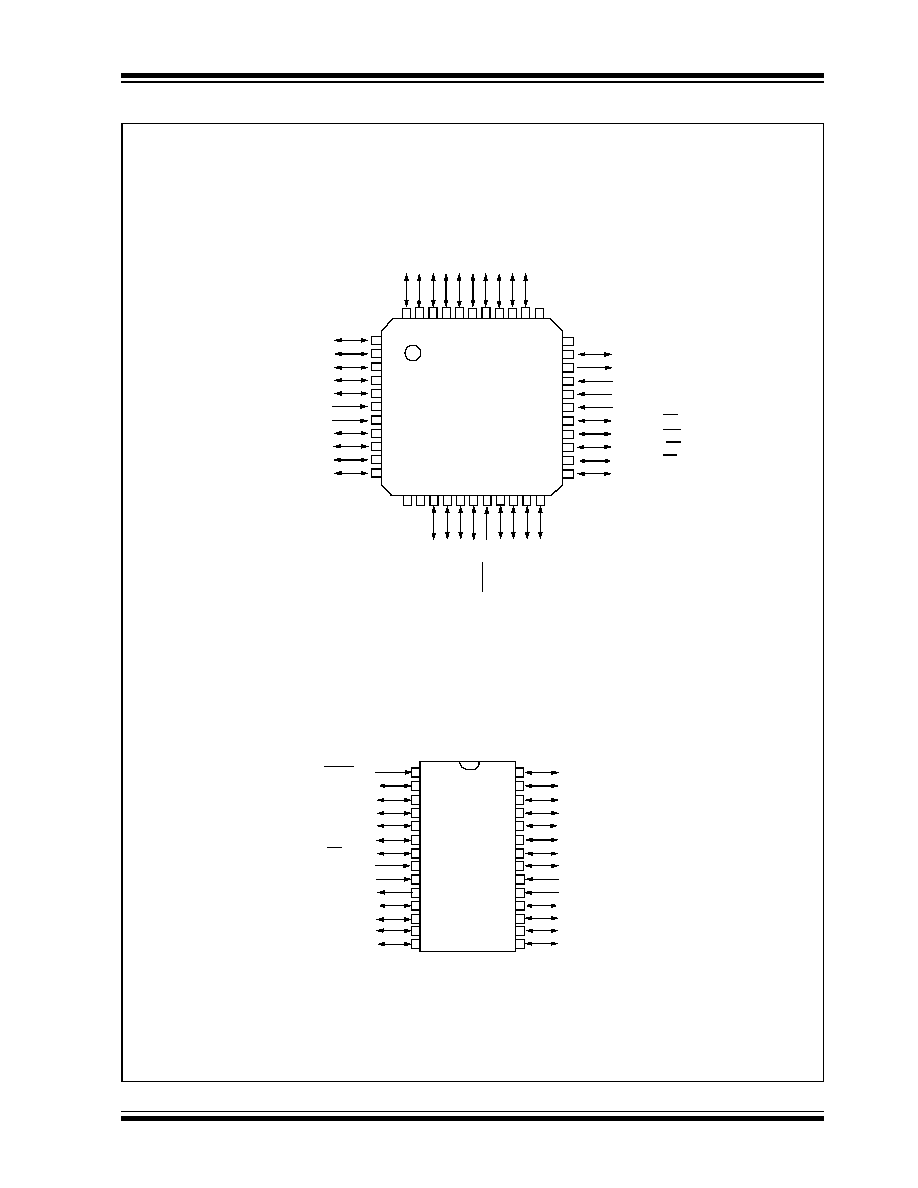
PIC18FXX8
Pin Diagrams (Continued)
PIC18F458
TQFP
RB7/PGD
SPDIP, SOIC
1
2
3
4
5
6
7
8
9
10
11
12
13
14
15
16
17
18
19
20
21
22
23
24
25
26
27
28
RB6/PGC
RB5/PGM
RB4
RB3/CANRX
RB2/CANTX/INT2
RB1/INT1
RB0/INT0
V
DD
V
SS
RC7/RX/DT
RC6/TX/CK
RC5/SDO
RC4/SDI/SDA
MCLR/V
PP
RA0/AN0/CV
REF
RA1/AN1
RA2/AN2/V
REF
-
RA3/AN3/V
REF
+
RA4/T0CKI
RA5/AN4/SS/LVDIN
V
SS
OSC1/CLKI
OSC2/CLKO/RA6
RC0/T1OSO/T1CKI
RC1/T1OSI
RC2/CCP1
RC3/SCK/SCL
PIC1
8F2
5
8
1
2
3
4
5
6
7
8
9
10
11
13
14
15
16
17
18
19
20
21
22
23
24
25
26
27
28
29
30
31
32
33
34
35
36
37
38
39
40
41
42
43
44
12
RC7/RX/DT
RD4/PSP4/ECCP1/P1A
RD5/PSP5/P1B
RD6/PSP6/P1C
RD7/PSP7/P1D
V
SS
V
DD
RB0/INT0
RB1/INT1
RB2/CANTX/INT2
RB3/CANRX
NC
NC
RB4
RB5
/
PG
M
RB
6
/
P
G
C
RB
7
/
P
G
D
MC
LR
/V
PP
RA
0/
A
N
0/
CV
RE
F
RA1
/
AN1
RA2
/
AN2
/
V
RE
F
-
R
A
3/
A
N
3/V
RE
F
+
NC
RC0/T1OSO/T1CKI
OSC1/CLKI
V
SS
V
DD
RE2/AN7/CS/C2OUT
RE1/AN6/WR/C1OUT
OSC2/CLKO/RA6
RE0//AN5/RD
RA5/AN4/SS/LVDIN
RA4/T0CKI
RC6
/T
X
/
CK
RC5
/
S
DO
RC
4
/
SDI/SDA
RD3
/
PSP3
/
C
2
I
N-
RD2
/
P
SP2
/C2
I
N+
RD
1
/
PSP1
/
C
1
I
N-
RD0
/
PSP0
/
C
1
I
N+
RC3
/SCK/SCL
RC2
/
CCP1
RC
1
/
T
1
OSI
NC
PIC18F448
PIC1
8F2
5
8

PIC18FXX8
DS41159B-page 4
Preliminary
2002 Microchip Technology Inc.
Table of Contents
1.0
Device Overview .......................................................................................................................................................................... 7
2.0
Oscillator Configurations ............................................................................................................................................................ 17
3.0
Reset .......................................................................................................................................................................................... 25
4.0
Memory Organization ................................................................................................................................................................. 37
5.0
Data EEPROM Memory ............................................................................................................................................................ 59
6.0
FLASH Program Memory ........................................................................................................................................................... 65
7.0
8 X 8 Hardware Multiplier ........................................................................................................................................................... 75
8.0
Interrupts .................................................................................................................................................................................... 77
9.0
I/O Ports ..................................................................................................................................................................................... 93
10.0 Parallel Slave Port .................................................................................................................................................................... 105
11.0 Timer0 Module ......................................................................................................................................................................... 107
12.0 Timer1 Module ......................................................................................................................................................................... 111
13.0 Timer2 Module ......................................................................................................................................................................... 115
14.0 Timer3 Module ......................................................................................................................................................................... 117
15.0 Capture/Compare/PWM (CCP) Modules ................................................................................................................................. 121
16.0 Enhanced Capture/Compare/PWM (ECCP) Module................................................................................................................ 129
17.0 Master Synchronous Serial Port (MSSP) Module .................................................................................................................... 141
18.0 Addressable Universal Synchronous Asynchronous Receiver Transmitter (USART).............................................................. 181
19.0 CAN Module ............................................................................................................................................................................. 197
20.0 Compatible 10-bit Analog-to-Digital Converter (A/D) Module................................................................................................... 237
21.0 Comparator Module.................................................................................................................................................................. 245
22.0 Comparator Voltage Reference Module ................................................................................................................................... 251
23.0 Low Voltage Detect .................................................................................................................................................................. 255
24.0 Special Features of the CPU .................................................................................................................................................... 261
25.0 Instruction Set Summary .......................................................................................................................................................... 277
26.0 Development Support............................................................................................................................................................... 319
27.0 Electrical Characteristics .......................................................................................................................................................... 325
28.0 DC and AC Characteristics Graphs and Tables ....................................................................................................................... 355
29.0 Packaging Information.............................................................................................................................................................. 357
Appendix A: Data Sheet Revision History.......................................................................................................................................... 365
Appendix B: Device Differences......................................................................................................................................................... 365
Appendix C: Device Migrations .......................................................................................................................................................... 366
Appendix D: Migrating from other PICmicro Devices......................................................................................................................... 366
Appendix E: Development Tool Version Requirements ..................................................................................................................... 367
Index .................................................................................................................................................................................................. 369
On-Line Support................................................................................................................................................................................. 379
Reader Response .............................................................................................................................................................................. 380
PIC18FXX8 Product Identification System......................................................................................................................................... 381

2002 Microchip Technology Inc.
Preliminary
DS41159B-page 5
PIC18FXX8
TO OUR VALUED CUSTOMERS
It is our intention to provide our valued customers with the best documentation possible to ensure successful use of your Microchip
products. To this end, we will continue to improve our publications to better suit your needs. Our publications will be refined and
enhanced as new volumes and updates are introduced.
If you have any questions or comments regarding this publication, please contact the Marketing Communications Department via
E-mail at docerrors@mail.microchip.com or fax the Reader Response Form in the back of this data sheet to (480) 792-4150.
We welcome your feedback.
Most Current Data Sheet
To obtain the most up-to-date version of this data sheet, please register at our Worldwide Web site at:
http://www.microchip.com
You can determine the version of a data sheet by examining its literature number found on the bottom outside corner of any page.
The last character of the literature number is the version number, (e.g., DS30000A is version A of document DS30000).
Errata
An errata sheet, describing minor operational differences from the data sheet and recommended workarounds, may exist for current
devices. As device/documentation issues become known to us, we will publish an errata sheet. The errata will specify the revision
of silicon and revision of document to which it applies.
To determine if an errata sheet exists for a particular device, please check with one of the following:
� Microchip's Worldwide Web site; http://www.microchip.com
� Your local Microchip sales office (see last page)
� The Microchip Corporate Literature Center; U.S. FAX: (480) 792-7277
When contacting a sales office or the literature center, please specify which device, revision of silicon and data sheet (include
literature number) you are using.
Customer Notification System
Register on our web site at www.microchip.com/cn to receive the most current information on all of our products.

PIC18FXX8
DS41159B-page 6
Preliminary
2002 Microchip Technology Inc.
NOTES:

2002 Microchip Technology Inc.
Preliminary
DS41159B-page 7
PIC18FXX8
1.0
DEVICE OVERVIEW
This document contains device specific information for
the following devices:
1.
PIC18F248
2.
PIC18F258
3.
PIC18F448
4.
PIC18F458
These devices are available in 28-pin, 40-pin and
44-pin packages. They are differentiated from each
other in four ways:
1.
PIC18FX58 devices have twice the FLASH pro-
gram memory and data RAM of PIC18FX48
devices (32 Kbytes and 1536 bytes vs.
16 Kbytes and 768 bytes, respectively).
2.
PIC18F2X8 devices implement 5 A/D channels,
as opposed to 8 for PIC18F4X8 devices.
3.
PIC18F2X8 devices implement 3 I/O ports,
while PIC18F4X8 devices implement 5.
4.
Only PIC18F4X8 devices implement the
Enhanced CCP module, analog comparators
and the Parallel Slave Port.
All other features for devices in the PIC18FXX8 family,
including the serial communications modules, are
identical. These are summarized in Table 1-1.
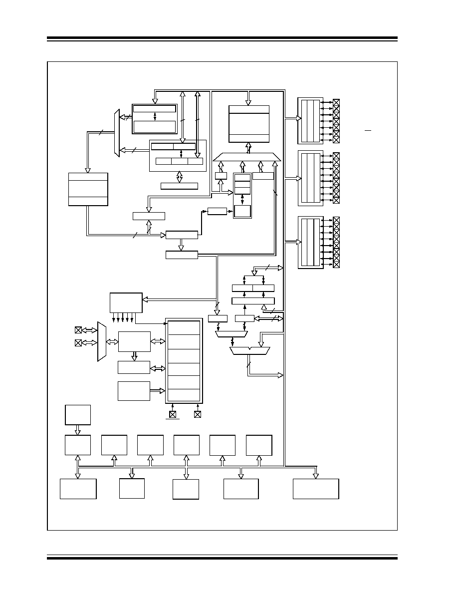
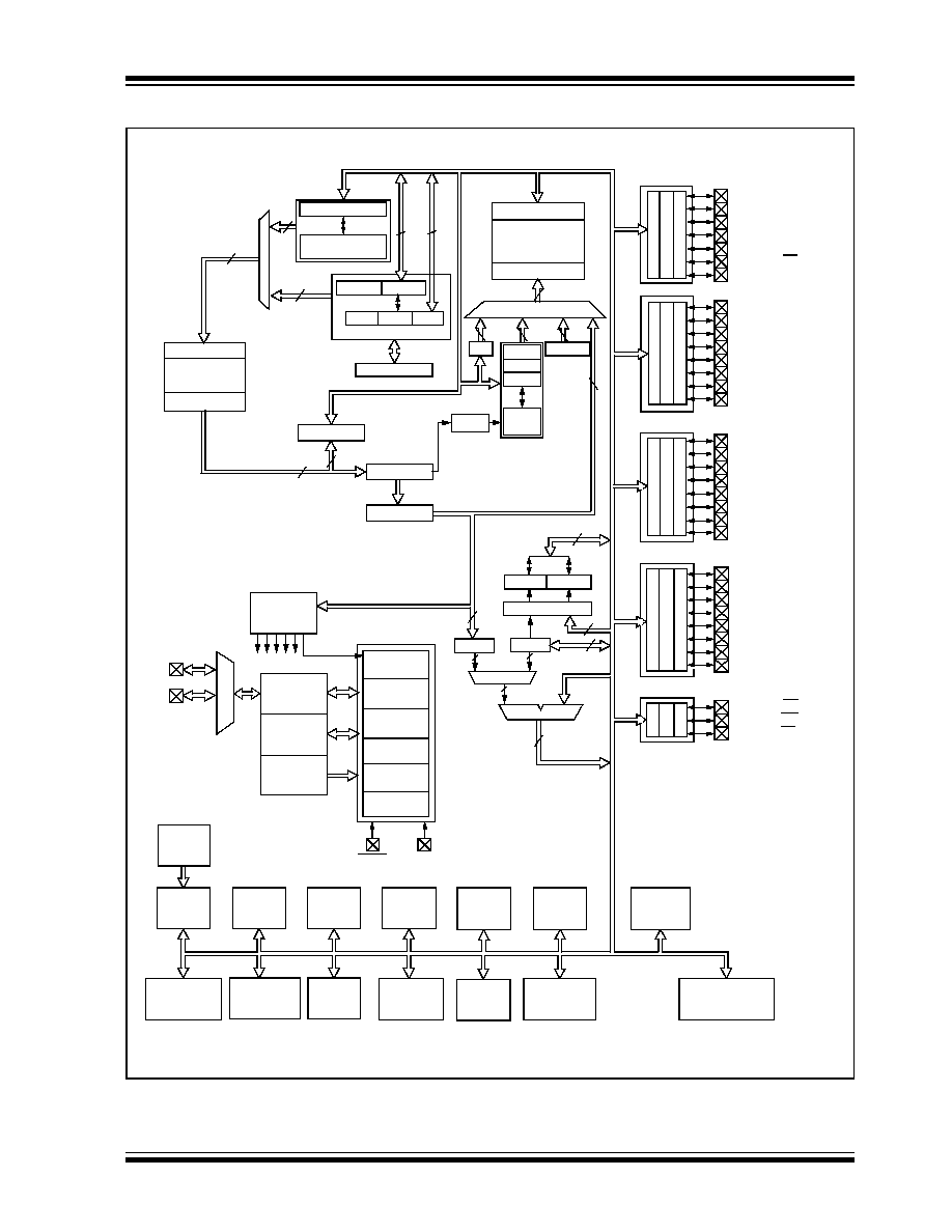
Block diagrams of the PIC18F2X8 and PIC18F4X8
devices are provided in Figure 1-1 and Figure 1-2,
respectively. The pinouts for these device families are
listed in Table 1-2.
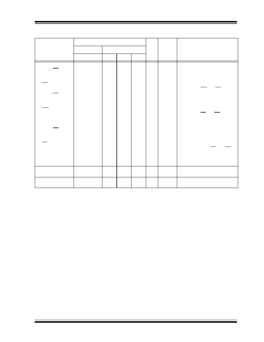
TABLE 1-1:
PIC18FXX8 DEVICE FEATURES
Features
PIC18F248
PIC18F258
PIC18F448
PIC18F458
Operating Frequency
DC - 40 MHz
DC - 40 MHz
DC - 40 MHz
DC - 40 MHz
Internal Program
Memory
Bytes
16K
32K
16K
32K
# of Single Word
Instructions
8192
16384
8192
16384
Data Memory (Bytes)
768
1536
768
1536
Data EEPROM Memory (Bytes)
256
256
256
256
Interrupt Sources
17
17
21
21
I/O Ports
Ports A, B, C
Ports A, B, C
Ports A, B, C, D, E Ports A, B, C, D, E
Timers
4
4
4
4
Capture/Compare/PWM Modules
1
1
1
1
Enhanced Capture/Compare/PWM
Modules
--
--
1
1
Serial Communications
MSSP, CAN,
Addressable
USART
MSSP, CAN,
Addressable
USART
MSSP, CAN,
Addressable
USART
MSSP, CAN,
Addressable
USART
Parallel Communications (PSP)
No
No
Yes
Yes
10-bit Analog-to-Digital Converter
5 input channels
5 input channels
8 input channels
8 input channels
Analog Comparators
No
No
2
2
Analog Comparators V
REF
Output
N/A
N/A
Yes
Yes
RESETS (and Delays)
POR, BOR,
RESET
Instruction,
Stack Full,
Stack Underflow
(PWRT, OST)
POR, BOR,
RESET
Instruction,
Stack Full,
Stack Underflow
(PWRT, OST)
POR, BOR,
RESET
Instruction,
Stack Full,
Stack Underflow
(PWRT, OST)
POR, BOR,
RESET
Instruction,
Stack Full,
Stack Underflow
(PWRT, OST)
Programmable Low Voltage Detect
Yes
Yes
Yes
Yes
Programmable Brown-out Reset
Yes
Yes
Yes
Yes
CAN Module
Yes
Yes
Yes
Yes
In-Circuit Serial ProgrammingTM
(ICSPTM)
Yes
Yes
Yes
Yes
Instruction Set
75 Instructions
75 Instructions
75 Instructions
75 Instructions
Packages
28-pin SPDIP
28-pin SOIC
28-pin SPDIP
28-pin SOIC
40-pin PDIP
44-pin PLCC
44-pin TQFP
40-pin PDIP
44-pin PLCC
44-pin TQFP
PIC18FXX8
DS41159B-page 8
Preliminary
2002 Microchip Technology Inc.
FIGURE 1-1:
PIC18F248/258 BLOCK DIAGRAM
Power-up
Timer
Oscillator
Start-up Timer
Power-on
Reset
Watchdog
Timer
Instruction
Decode &
Control
OSC1/CLKI
OSC2/CLKO/RA6
MCLR
V
DD
,
V
SS
PORTA
PORTB
PORTC
RA4/T0CKI
RA5/AN4/SS/LVDIN
RB0/INT0
RB4
RC0/T1OSO/T1CKI
RC1/T1OSI
RC2/CCP1
RC3/SCK/SCL
RC4/SDI/SDA
RC5/SDO
RC6/TX/CK
RC7/RX/DT
Brown-out
Reset
Synchronous
Timer0
Timer1
Timer2
Serial Port
RA3/AN3/V
REF
+
RA2/AN2/V
REF
-
RA1/AN1
RA0/AN0/CV
REF
CAN Module
Timing
Generation
10-bit
ADC
RB1/INT1
Data Latch
Data RAM
up to 1536 bytes
Address Latch
Address<12>
12
Bank0, F
BSR
FSR0
FSR1
FSR2
inc/dec
logic
Decode
4
12
4
PCH
PCL
PCLATH
8
31 Level Stack
Program Counter
PRODH
8 x 8 Multiply
W
8
BITOP
8
8
ALU<8>
8
Test Mode
Select
Address Latch
Program Memory
up to 32 Kbytes
Data Latch
21
21
16
8
8
8
Table Pointer<21>
inc/dec logic
21
8
Data Bus<8>
Table Latch
8
IR
12
3
ROM Latch
Timer3
RB2/CANTX/INT2
RB3/CANRX
T1OSI
T1OSO
PCLATU
PCU
Precision
Reference
Bandgap
RB7/PGD
RB5/PGM
RB6/PGC
PBOR
PLVD
CCP1
4X PLL
Bandgap
OSC2/CLKO/RA6
PRODL
Data EEPROM
USART
2002 Microchip Technology Inc.
Preliminary
DS41159B-page 9
PIC18FXX8
FIGURE 1-2:
PIC18F448/458 BLOCK DIAGRAM
Power-up
Timer
Oscillator
Start-up Timer
Power-on
Reset
Watchdog
Timer
Instruction
Decode &
Control
OSC1/CLKI
OSC2/CLKO/RA6
MCLR
V
DD
, V
SS
PORTA
PORTB
PORTC
RA4/T0CKI
RA5/AN4/SS/LVDIN
RB0/INT0
RB4
RC0/T1OSO/T1CKI
RC1/T1OSI
RC2/CCP1
RC3/SCK/SCL
RC4/SDI/SDA
RC5/SDO
RC6/TX/CK
RC7/RX/DT
Brown-out
Reset
Comparators
RA3/AN3/V
REF
+
RA2/AN2/V
REF
-
RA1/AN1
RA0/AN0/CV
REF
Timing
Generation
RB1/INT1
Data Latch
Data RAM
up to 1536 Kbytes
Address Latch
Address<12>
12
Bank0, F
BSR
FSR0
FSR1
FSR2
inc/dec
logic
Decode
4
12
4
PCH
PCL
PCLATH
8
31 Level Stack
Program Counter
PRODL
PRODH
8 x 8 Multiply
W
8
BITOP
8
8
ALU<8>
8
Test Mode
Select
Address Latch
Program Memory
up to 32 Kbytes
Data Latch
21
21
16
8
8
8
Table Pointer<21>
inc/dec logic
21
8
Data Bus<8>
Table Latch
8
IR
12
3
ROM Latch
PORTD
RD0/PSP0/C1IN+
Enhanced
RB2/CANTX/INT2
RB3/CANRX
T1OSI
T1OSO
PCLATU
PCU
Precision
Reference
Bandgap
PORTE
RE0/AN5/RD
CCP
RB7/PGD
RB5/PGM
RB6/PGC
RD4/PSP4/ECCP1/P1A
RD5/PSP5/P1B
RD6/PSP6/P1C
RD7/PSP7/P1D
RE1/AN6/WR//C1OUT
RE2/AN7/CS/C2OUT
RD1/PSP1/C1IN-
RD2/PSP2/C2IN+
RD3/PSP3/C2IN-
4X
PLL
Bandgap
OSC2/CLKO/RA6
USART
Synchronous
Timer0
Timer1
Timer2
Serial Port
CAN Module
10-bit
ADC
Timer3
PBOR
PLVD
CCP1
Data EEPROM
USART
Parallel
Slave Port

PIC18FXX8
DS41159B-page 10
Preliminary
2002 Microchip Technology Inc.
TABLE 1-2:
PIC18FXX8 PINOUT I/O DESCRIPTIONS
Pin Name
Pin Number
Pin
Type
Buffer
Type
Description
PIC18F248/258
PIC18F448/458
SPDIP, SOIC
PDIP
TQFP
PLCC
MCLR/V
PP
MCLR
V
PP
1
1
18
2
I
P
ST
--
Master Clear (input) or
programming voltage (output).
Master Clear (Reset) input.
This pin is an active low
RESET to the device.
Programming voltage input.
NC
--
--
12, 13,
33, 34
1, 17,
28, 40
--
--
These pins should be left
unconnected.
OSC1/CLKI
OSC1
CLKI
9
13
30
14
I
I
CMOS/ST
CMOS
Oscillator crystal or external clock
input.
Oscillator crystal input or
external clock source input. ST
buffer when configured in RC
mode. Otherwise CMOS.
External clock source input.
Always associated with pin
function OSC1 (see OSC1/
CLKI, OSC2/CLKO pins).
OSC2/CLKO/RA6
OSC2
CLKO
RA6
10
14
31
15
O
O
I/O
--
--
TTL
Oscillator crystal or clock output.
Oscillator crystal output.
Connects to crystal or
resonator in Crystal Oscillator
mode.
In RC mode, OSC2 pin outputs
CLKO, which has 1/4 the
frequency of OSC1 and
denotes the instruction cycle
rate.
General purpose I/O pin.
Legend:
TTL =
TTL compatible input
CMOS = CMOS compatible input or output
ST =
Schmitt Trigger input with CMOS levels Analog = Analog input
I
=
Input O
= Output
P
=
Power
OD
= Open Drain (no P diode to V
DD
)

2002 Microchip Technology Inc.
Preliminary
DS41159B-page 11
PIC18FXX8
PORTA is a bi-directional I/O port.
RA0/AN0/C
VREF
RA0
AN0
C
VREF
2
2
19
3
I/O
I
O
TTL
Analog
Analog
Digital I/O.
Analog input 0.
Comparator voltage reference
output.
RA1/AN1
RA1
AN1
3
3
20
4
I/O
I
TTL
Analog
Digital I/O.
Analog input 1.
RA2/AN2/V
REF
-
RA2
AN2
V
REF
-
4
4
21
5
I/O
I
I
TTL
Analog
Analog
Digital I/O.
Analog input 2.
A/D reference voltage
(Low) input.
RA3/AN3/V
REF
+
RA3
AN3
V
REF
+
5
5
22
6
I/O
I
I
TTL
Analog
Analog
Digital I/O.
Analog input 3.
A/D reference voltage
(High) input.
RA4/T0CKI
RA4
T0CKI
6
6
23
7
I/O
I
TTL/OD
ST
Digital I/O - open drain when
configured as output.
Timer0 external clock input.
RA5/AN4/SS/LVDIN
RA5
AN4
SS
LVDIN
7
7
24
8
I/O
I
I
I
TTL
Analog
ST
Analog
Digital I/O.
Analog input 4.
SPI slave select input.
Low voltage detect input.
RA6
See the OSC2/CLKO/RA6 pin.
TABLE 1-2:
PIC18FXX8 PINOUT I/O DESCRIPTIONS (CONTINUED)
Pin Name
Pin Number
Pin
Type
Buffer
Type
Description
PIC18F248/258
PIC18F448/458
SPDIP, SOIC
PDIP
TQFP
PLCC
Legend:
TTL =
TTL compatible input
CMOS = CMOS compatible input or output
ST =
Schmitt Trigger input with CMOS levels Analog = Analog input
I
=
Input O
= Output
P
=
Power
OD
= Open Drain (no P diode to V
DD
)

PIC18FXX8
DS41159B-page 12
Preliminary
2002 Microchip Technology Inc.
PORTB is a bi-directional I/O port.
PORTB can be software
programmed for internal weak
pull-ups on all inputs.
RB0/INT0
RB0
INT0
21
33
8
36
I/O
I
TTL
ST
Digital I/O.
External interrupt 0.
RB1/INT1
RB1
INT1
22
34
9
37
I/O
I
TTL
ST
Digital I/O.
External interrupt 1.
RB2/CANTX/INT2
RB2
CANTX
INT2
23
35
10
38
I/O
O
I
TTL
TTL
ST
Digital I/O.
Transmit signal for CAN bus.
External interrupt 2.
RB3/CANRX
RB3
CANRX
24
36
11
39
I/O
I
TTL
TTL
Digital I/O.
Receive signal for CAN bus.
RB4
25
37
14
41
I/O
TTL
Digital I/O.
Interrupt-on-change pin.
RB5/PGM
RB5
PGM
26
38
15
42
I/O
I
TTL
ST
Digital I/O.
Interrupt-on-change pin.
Low voltage ICSP
programming enable.
RB6/PGC
RB6
PGC
27
39
16
43
I/O
I
TTL
ST
Digital I/O. In-Circuit
Debugger pin.
Interrupt-on-change pin.
ICSP programming clock.
RB7/PGD
RB7
PGD
28
40
17
44
I/O
I/O
TTL
ST
Digital I/O. In-Circuit
Debugger pin.
Interrupt-on-change pin.
ICSP programming data.
TABLE 1-2:
PIC18FXX8 PINOUT I/O DESCRIPTIONS (CONTINUED)
Pin Name
Pin Number
Pin
Type
Buffer
Type
Description
PIC18F248/258
PIC18F448/458
SPDIP, SOIC
PDIP
TQFP
PLCC
Legend:
TTL =
TTL compatible input
CMOS = CMOS compatible input or output
ST =
Schmitt Trigger input with CMOS levels Analog = Analog input
I
=
Input O
= Output
P
=
Power
OD
= Open Drain (no P diode to V
DD
)

2002 Microchip Technology Inc.
Preliminary
DS41159B-page 13
PIC18FXX8
PORTC is a bi-directional I/O port.
RC0/T1OSO/T1CKI
RC0
T1OSO
T1CKI
11
15
32
16
I/O
O
I
ST
--
ST
Digital I/O.
Timer1 oscillator output.
Timer1/Timer3 external clock
input.
RC1/T1OSI
RC1
T1OSI
12
16
35
18
I/O
I
ST
CMOS
Digital I/O.
Timer1 oscillator input.
RC2/CCP1
RC2
CCP1
13
17
36
19
I/O
I/O
ST
ST
Digital I/O.
Capture1 input/Compare1
output/PWM1 output.
RC3/SCK/SCL
RC3
SCK
SCL
14
18
37
20
I/O
I/O
I/O
ST
ST
ST
Digital I/O.
Synchronous serial clock
input/output for SPI mode.
Synchronous serial clock
input/output for I
2
C mode.
RC4/SDI/SDA
RC4
SDI
SDA
15
23
42
25
I/O
I
I/O
ST
ST
ST
Digital I/O.
SPI data in.
I
2
C data I/O.
RC5/SDO
RC5
SDO
16
24
43
26
I/O
O
ST
--
Digital I/O.
SPI data out.
RC6/TX/CK
RC6
TX
CK
17
25
44
27
I/O
O
I/O
ST
--
ST
Digital I/O.
USART asynchronous
transmit.
USART synchronous clock
(see RX/DT).
RC7/RX/DT
RC7
RX
DT
18
26
1
29
I/O
I
I/O
ST
ST
ST
Digital I/O.
USART asynchronous receive.
USART synchronous data
(see TX/CK).
TABLE 1-2:
PIC18FXX8 PINOUT I/O DESCRIPTIONS (CONTINUED)
Pin Name
Pin Number
Pin
Type
Buffer
Type
Description
PIC18F248/258
PIC18F448/458
SPDIP, SOIC
PDIP
TQFP
PLCC
Legend:
TTL =
TTL compatible input
CMOS = CMOS compatible input or output
ST =
Schmitt Trigger input with CMOS levels Analog = Analog input
I
=
Input O
= Output
P
=
Power
OD
= Open Drain (no P diode to V
DD
)

PIC18FXX8
DS41159B-page 14
Preliminary
2002 Microchip Technology Inc.
PORTD is a bi-directional I/O port.
These pins have TTL input buffers
when external memory is enabled.
RD0/PSP0/C1IN+
RD0
PSP0
C1IN+
--
19
38
21
I/O
I/O
I
ST
TTL
Analog
Digital I/O.
Parallel slave port data.
Comparator 1 input.
RD1/PSP1/C1IN-
RD1
PSP1
C1IN-
--
20
39
22
I/O
I/O
I
ST
TTL
Analog
Digital I/O.
Parallel slave port data.
Comparator 1 input.
RD2/PSP2/C2IN+
RD2
PSP2
C2IN+
--
21
40
23
I/O
I/O
I
ST
TTL
Analog
Digital I/O.
Parallel slave port data.
Comparator 2 input.
RD3/PSP3/C2IN-
RD3
PSP3
C2IN-
--
22
41
24
I/O
I/O
I
ST
TTL
Analog
Digital I/O.
Parallel slave port data.
Comparator 2 input.
RD4/PSP4/ECCP1/
P1A
RD4
PSP4
ECCP1
P1A
--
27
2
30
I/O
I/O
I/O
O
ST
TTL
ST
--
Digital I/O.
Parallel slave port data.
ECCP1 capture/compare.
ECCP1 PWM output A.
RD5/PSP5/P1B
RD5
PSP5
P1B
--
28
3
31
I/O
I/O
O
ST
TTL
--
Digital I/O.
Parallel slave port data.
ECCP1 PWM output B.
RD6/PSP6/P1C
RD6
PSP6
P1C
--
29
4
32
I/O
I/O
O
ST
TTL
--
Digital I/O.
Parallel slave port data.
ECCP1 PWM output C.
RD7/PSP7/P1D
RD7
PSP7
P1D
--
30
5
33
I/O
I/O
O
ST
TTL
--
Digital I/O.
Parallel slave port data.
ECCP1 PWM output D.
TABLE 1-2:
PIC18FXX8 PINOUT I/O DESCRIPTIONS (CONTINUED)
Pin Name
Pin Number
Pin
Type
Buffer
Type
Description
PIC18F248/258
PIC18F448/458
SPDIP, SOIC
PDIP
TQFP
PLCC
Legend:
TTL =
TTL compatible input
CMOS = CMOS compatible input or output
ST =
Schmitt Trigger input with CMOS levels Analog = Analog input
I
=
Input O
= Output
P
=
Power
OD
= Open Drain (no P diode to V
DD
)
2002 Microchip Technology Inc.
Preliminary
DS41159B-page 15
PIC18FXX8
PORTE is a bi-directional I/O port.
RE0/AN5/RD
RE0
AN5
RD
--
8
25
9
I/O
I
I
ST
Analog
TTL
Digital I/O.
Analog input 5.
Read control for parallel slave
port (see WR and CS pins).
RE1/AN6/WR/C1OUT
RE1
AN6
WR
C1OUT
--
9
26
10
I/O
I
I
O
ST
Analog
TTL
Analog
Digital I/O.
Analog input 6.
Write control for parallel slave
port (see CS and RD pins).
Comparator 1 output.
RE2/AN7/CS/C2OUT
RE2
AN7
CS
C2OUT
--
10
27
11
I/O
I
I
O
ST
Analog
TTL
Analog
Digital I/O.
Analog input 7.
Chip select control for parallel
slave port (see RD and WR
pins).
Comparator 2 output.
V
SS
19, 8
12, 31
6, 29
13, 34
--
--
Ground reference for logic and
I/O pins.
V
DD
20
11, 32
7, 28
12, 35
--
--
Positive supply for logic and I/O
pins.
TABLE 1-2:
PIC18FXX8 PINOUT I/O DESCRIPTIONS (CONTINUED)
Pin Name
Pin Number
Pin
Type
Buffer
Type
Description
PIC18F248/258
PIC18F448/458
SPDIP, SOIC
PDIP
TQFP
PLCC
Legend:
TTL =
TTL compatible input
CMOS = CMOS compatible input or output
ST =
Schmitt Trigger input with CMOS levels Analog = Analog input
I
=
Input O
= Output
P
=
Power
OD
= Open Drain (no P diode to V
DD
)

PIC18FXX8
DS41159B-page 16
Preliminary
2002 Microchip Technology Inc.
NOTES:
2002 Microchip Technology Inc.
Preliminary
DS41159B-page 17
PIC18FXX8
2.0
OSCILLATOR
CONFIGURATIONS
2.1
Oscillator Types
The PIC18FXX8 can be operated in one of eight Oscil-
lator modes, programmable by three configuration bits
(FOSC2, FOSC1, and FOSC0).
1.
LP
Low Power Crystal
2.
XT
Crystal/Resonator
3.
HS
High Speed Crystal/Resonator
4.
HS4
High Speed Crystal/Resonator with
PLL enabled
5.
RC
External Resistor/Capacitor
6.
RCIO
External Resistor/Capacitor with I/O
pin enabled
7.
EC
External Clock
8.
ECIO
External Clock with I/O pin enabled
2.2
Crystal Oscillator/Ceramic
Resonators
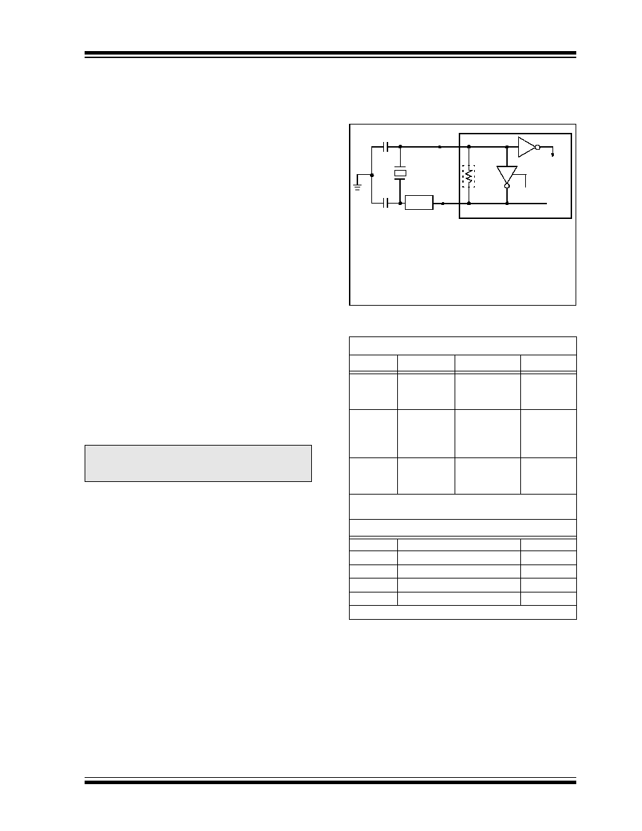
In XT, LP, HS or HS4 (PLL) Oscillator modes, a crystal
or ceramic resonator is connected to the OSC1 and
OSC2 pins to establish oscillation. Figure 2-1 shows
the pin connections. An external clock source may also
be connected to the OSC1 pin, as shown in Figure 2-3
and Figure 2-4.
The PIC18FXX8 oscillator design requires the use of a
parallel cut crystal.
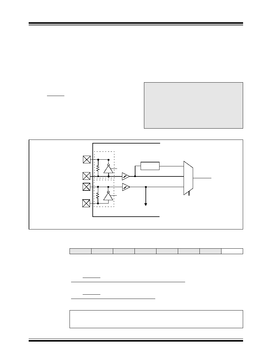
FIGURE 2-1:
CRYSTAL/CERAMIC
RESONATOR OPERATION
(HS, XT OR LP OSC
CONFIGURATION)
TABLE 2-1:
CERAMIC RESONATORS
Note:
Use of a series cut crystal may give a fre-
quency out of the crystal manufacturer's
specifications.
Ranges Tested:
Mode
Freq
OSC1
OSC2
XT
455 kHz
2.0 MHz
4.0 MHz
68 - 100 pF
15 - 68 pF
15 - 68 pF
68 - 100 pF
15 - 68 pF
15 - 68 pF
HS
8.0 MHz
16.0 MHz
20.0 MHz
25.0 MHz
10 - 68 pF
10 - 22 pF
TBD
TBD
10 - 68 pF
10 - 22 pF
TBD
TBD
HS+PLL
4.0 MHz
8.0 MHz
10.0 MHz
TBD
10 - 68 pF
TBD
TBD
10 - 68 pF
TBD
These values are for design guidance only.
See notes following Table 2-2.
Resonators Used:
455 kHz
Panasonic EFO-A455K04B
�
0.3%
2.0 MHz
Murata Erie CSA2.00MG
�
0.5%
4.0 MHz
Murata Erie CSA4.00MG
�
0.5%
8.0 MHz
Murata Erie CSA8.00MT
�
0.5%
16.0 MHz
Murata Erie CSA16.00MX
�
0.5%
All resonators used did not have built-in capacitors.
Note 1: See Table 2-1 and Table 2-2 for recommended
values of C1 and C2.
2: A series resistor (R
S
) may be required for AT
strip cut crystals.
3: R
F
varies with the crystal chosen.
C1
(1)
C2
(1)
XTAL
OSC2
OSC1
R
F
(3)
SLEEP
To
Logic
PIC18FXX8
R
S
(2)
Internal
PIC18FXX8
DS41159B-page 18
Preliminary
2002 Microchip Technology Inc.
TABLE 2-2:
CAPACITOR SELECTION FOR
CRYSTAL OSCILLATOR
2.3
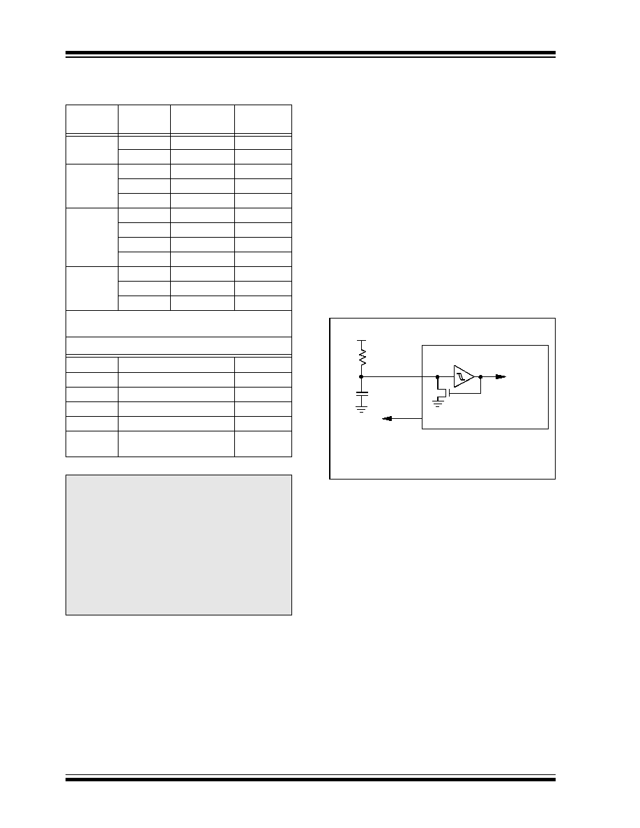
RC Oscillator
For timing insensitive applications, the "RC" and
"RCIO" device options offer additional cost savings.
The RC oscillator frequency is a function of the supply
voltage, the resistor (R
EXT
) and capacitor (C
EXT
) val-
ues and the operating temperature. In addition to this,
the oscillator frequency will vary from unit to unit due to
normal process parameter variation. Furthermore, the
difference in lead frame capacitance between package
types will also affect the oscillation frequency, espe-
cially for low C
EXT
values. The user also needs to take
into account variation due to tolerance of external R
and C components used. Figure 2-2 shows how the RC
combination is connected.
In the RC Oscillator mode, the oscillator frequency
divided by 4 is available on the OSC2 pin. This signal
may be used for test purposes or to synchronize other
logic.
FIGURE 2-2:
RC OSCILLATOR MODE
The RCIO Oscillator mode functions like the RC mode,
except that the OSC2 pin becomes an additional
general purpose I/O pin.
Osc Type
Crystal
Freq
Cap. Range
C1
Cap. Range
C2
LP
32.0 kHz
33 pF
33 pF
200 kHz
15 pF
15 pF
XT
200 kHz
47-68 pF
47-68 pF
1.0 MHz
15 pF
15 pF
4.0 MHz
15 pF
15 pF
HS
4.0 MHz
15 pF
15 pF
8.0 MHz
15-33 pF
15-33 pF
20.0 MHz
15-33 pF
15-33 pF
25.0 MHz
TBD
TBD
HS+PLL
4.0 MHz
15 pF
15 pF
8.0 MHz
15-33 pF
15-33 pF
10.0 MHz
TBD
TBD
These values are for design guidance only.
See notes on this page.
Crystals Used
32.0 kHz
Epson C-001R32.768K-A
� 20 PPM
200 kHz
STD XTL 200.000KHz
� 20 PPM
1.0 MHz
ECS ECS-10-13-1
� 50 PPM
4.0 MHz
ECS ECS-40-20-1
� 50 PPM
8.0 MHz
EPSON CA-301 8.000M-C
� 30 PPM
20.0 MHz
EPSON CA-301 20.000M-
C
� 30 PPM
Note 1: Recommended values of C1 and C2 are
identical to the ranges tested (Table 2-1).
2: Higher capacitance increases the stability
of the oscillator, but also increases the
start-up time.
3: Since each resonator/crystal has its own
characteristics, the user should consult the
resonator/crystal manufacturer for
appropriate values of external components.
4: Rs may be required in HS mode, as well as
XT mode, to avoid overdriving crystals with
low drive level specification.
OSC2/CLKO
C
EXT
R
EXT
PIC18FXX8
OSC1
F
OSC
/4
Internal
Clock
V
DD
V
SS
Recommended values:
3 k
R
EXT
100 k
C
EXT
>
20 pF
2002 Microchip Technology Inc.
Preliminary
DS41159B-page 19
PIC18FXX8
2.4
External Clock Input
The EC and ECIO Oscillator modes require an external
clock source to be connected to the OSC1 pin. The
feedback device between OSC1 and OSC2 is turned
off in these modes to save current. There is no oscilla-
tor start-up time required after a Power-on Reset or
after a recovery from SLEEP mode.
In the EC Oscillator mode, the oscillator frequency
divided by 4 is available on the OSC2 pin. This signal
may be used for test purposes or to synchronize other
logic. Figure 2-3 shows the pin connections for the EC
Oscillator mode.
FIGURE 2-3:
EXTERNAL CLOCK INPUT
OPERATION (EC OSC
CONFIGURATION)
The ECIO Oscillator mode functions like the EC mode,
except that the OSC2 pin becomes an additional gen-
eral purpose I/O pin. Figure 2-4 shows the pin connec-
tions for the ECIO Oscillator mode.
FIGURE 2-4:
EXTERNAL CLOCK INPUT
OPERATION (ECIO
CONFIGURATION)
2.5
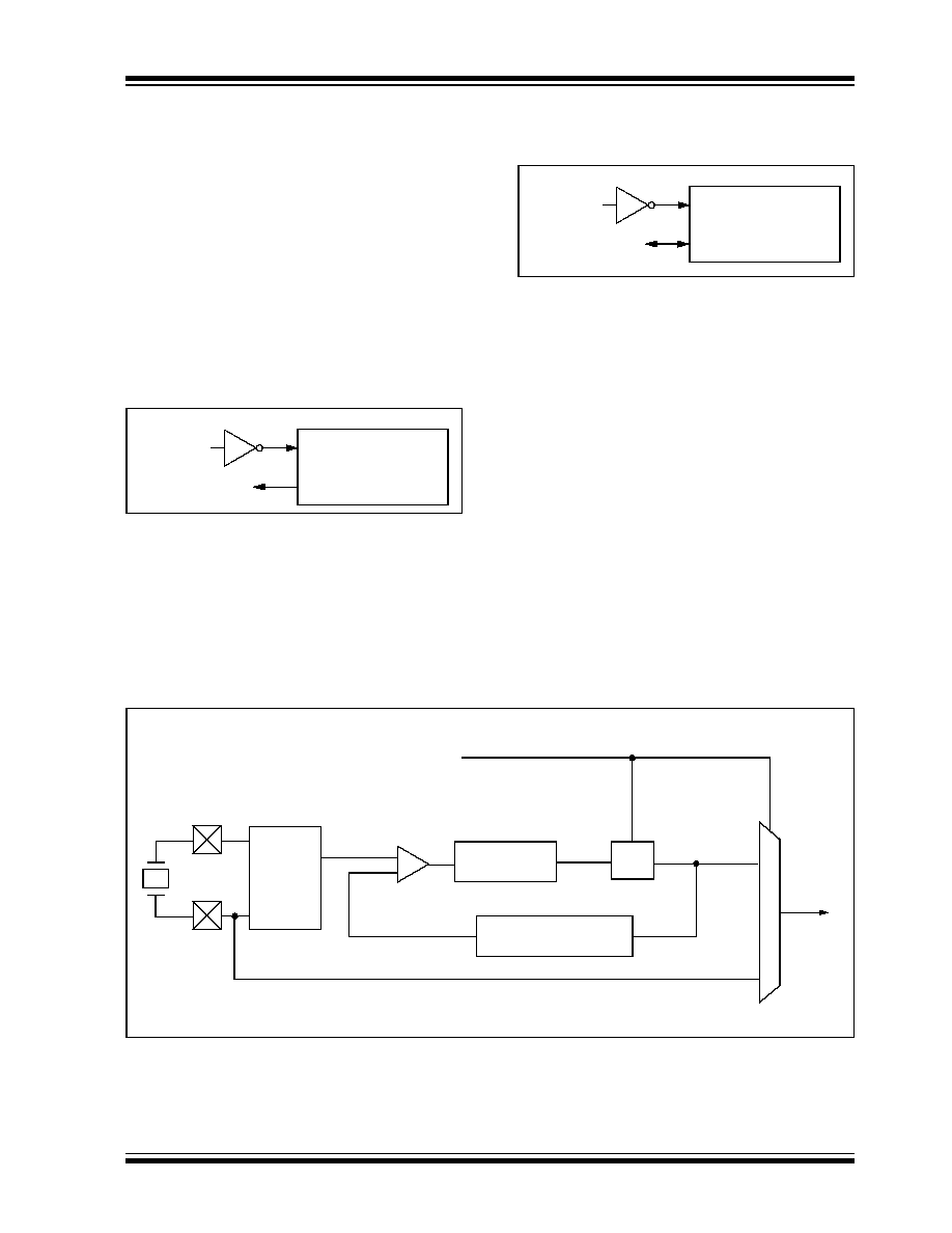
HS4 (PLL)
A Phase Locked Loop circuit is provided as a program-
mable option for users that want to multiply the fre-
quency of the incoming crystal oscillator signal by 4.
For an input clock frequency of 10 MHz, the internal
clock frequency will be multiplied to 40 MHz. This is
useful for customers who are concerned with EMI due
to high frequency crystals.
The PLL can only be enabled when the oscillator con-
figuration bits are programmed for HS mode. If they are
programmed for any other mode, the PLL is not
enabled and the system clock will come directly from
OSC1.
The PLL is one of the modes of the FOSC2:FOSC0
configuration bits. The Oscillator mode is specified dur-
ing device programming.
A PLL lock timer is used to ensure that the PLL has
locked before device execution starts. The PLL lock
timer has a time-out referred to as T
PLL
.
FIGURE 2-5:
PLL BLOCK DIAGRAM
OSC1
OSC2
F
OSC
/4
Clock from
Ext. System
PIC18FXX8
OSC1
I/O (OSC2)
Clock from
Ext. System
PIC18FXX8
MU
X
VCO
Loop
Filter
Divide by 4
Crystal
Osc
OSC2
OSC1
F
IN
F
OUT
SYSCLK
Phase
Comparator
FOSC2:FOSC0 = `
110
'
PIC18FXX8
DS41159B-page 20
Preliminary
2002 Microchip Technology Inc.
2.6
Oscillator Switching Feature
The PIC18FXX8 devices include a feature that allows
the system clock source to be switched from the main
oscillator to an alternate low frequency clock source.
For the PIC18FXX8 devices, this alternate clock source
is the Timer1 oscillator. If a low frequency crystal
(32 kHz, for example) has been attached to the Timer1
oscillator pins and the Timer1 oscillator has been
enabled, the device can switch to a Low Power Execu-
tion mode. Figure 2-6 shows a block diagram of the sys-
tem clock sources. The clock switching feature is
enabled by programming the Oscillator Switching
Enable (OSCSEN) bit in Configuration register,
CONFIG1H, to a '
0
'. Clock switching is disabled in an
erased device. See Section 12.2 for further details of
the Timer1 oscillator, and Section 24.1 for Configuration
Register details.
2.6.1
SYSTEM CLOCK SWITCH BIT
The system clock source switching is performed under
software control. The system clock switch bit, SCS
(OSCCON register), controls the clock switching. When
the SCS bit is '
0
', the system clock source comes from
the main oscillator selected by the FOSC2:FOSC0 con-
figuration bits. When the SCS bit is set, the system clock
source comes from the Timer1 oscillator. The SCS bit is
cleared on all forms of RESET.
FIGURE 2-6:
DEVICE CLOCK SOURCES
REGISTER 2-1:
OSCCON REGISTER
Note:
The Timer1 oscillator must be enabled to
switch the system clock source. The
Timer1 oscillator is enabled by setting the
T1OSCEN bit in the Timer1 control register
(T1CON). If the Timer1 oscillator is not
enabled, any write to the SCS bit will be
ignored (SCS bit forced cleared) and the
main oscillator continues to be the system
clock source.
U-0
U-0
U-0
U-0
U-0
U-0
U-0
R/W-0
--
--
--
--
--
--
--
SCS
bit 7
bit 0
bit 7-1
Unimplemented: Read as '0'
bit 0
SCS: System Clock Switch bit
When OSCSEN configuration bit = '0' and T1OSCEN bit is set:
1
= Switch to Timer1 oscillator/clock pin
0
= Use primary oscillator/clock input pin
When OSCSEN is clear or T1OSCEN is clear:
Bit is forced clear
Legend:
R = Readable bit
W = Writable bit
U = Unimplemented bit, read as `0'
- n = Value at POR
'1' = Bit is set
'0' = Bit is cleared
x = Bit is unknown
PIC18FXX8
T
OSC
4 x PLL
T
T
1
P
T
SCLK
Clock
Source
MUX
T
OSC
/4
Timer 1 Oscillator
T1OSCEN
Enable
Oscillator
T1OSO
T1OSI
Clock Source Option
for Other Modules
OSC1
OSC2
SLEEP
Main Oscillator
Note:
I/O pins have diode protection to V
DD
and V
SS
.
2002 Microchip Technology Inc.
Preliminary
DS41159B-page 21
PIC18FXX8
2.6.2
OSCILLATOR TRANSITIONS
The PIC18FXX8 devices contain circuitry to prevent
"glitches" when switching between oscillator sources.
Essentially, the circuitry waits for eight rising edges of
the clock source that the processor is switching to. This
ensures that the new clock source is stable and that its
pulse width will not be less than the shortest pulse
width of the two clock sources.
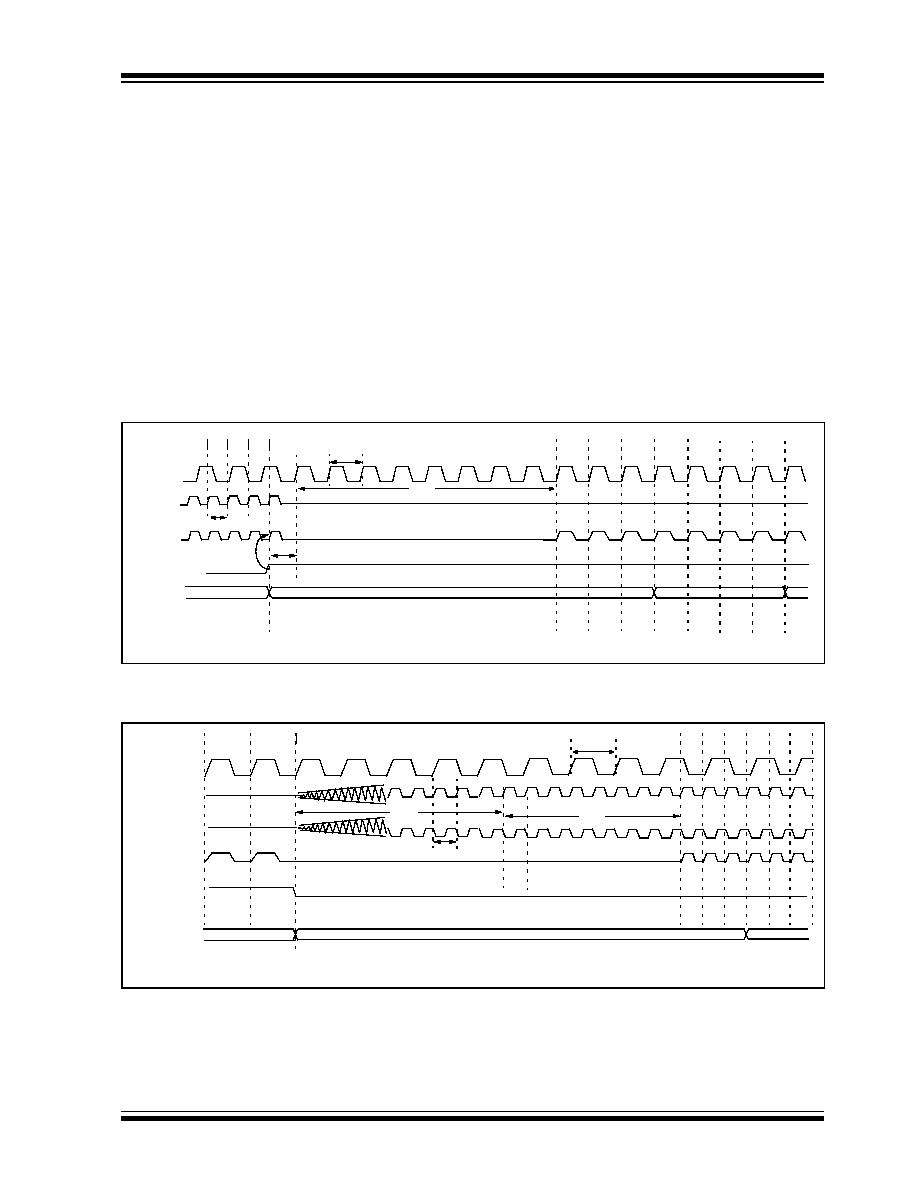
Figure 2-7 shows a timing diagram indicating the tran-
sition from the main oscillator to the Timer1 oscillator.
The Timer1 oscillator is assumed to be running all the
time. After the SCS bit is set, the processor is frozen at
the next occurring Q1 cycle. After eight synchronization
cycles are counted from the Timer1 oscillator, opera-
tion resumes. No additional delays are required after
the synchronization cycles.
The sequence of events that takes place when switch-
ing from the Timer1 oscillator to the main oscillator will
depend on the mode of the main oscillator. In addition
to eight clock cycles of the main oscillator, additional
delays may take place.
If the main oscillator is configured for an external crys-
tal (HS, XT, LP), the transition will take place after an
oscillator start-up time (T
OST
) has occurred. A timing
diagram indicating the transition from the Timer1 oscil-
lator to the main oscillator for HS, XT, and LP modes is
shown in Figure 2-8.
FIGURE 2-7:
TIMING DIAGRAM FOR TRANSITION FROM OSC1 TO TIMER1 OSCILLATOR
FIGURE 2-8:
TIMING DIAGRAM FOR TRANSITION BETWEEN TIMER1 AND OSC1 (HS, XT, LP)
Q3
Q2
Q1
Q4
Q3
Q2
OSC1
Internal
SCS
(OSCCON<0>)
Program
PC + 2
PC
Note 1: Delay on internal system clock is eight oscillator cycles for synchronization.
Q1
T1OSI
Q4
Q1
PC + 4
Q1
Tscs
Clock
Counter
System
Q2
Q3
Q4
Q1
T
DLY
T
T
1
P
T
OSC
2
1
3
4
5
6
7
8
Q3
Q3
Q4
Q1 Q2 Q3 Q4
Q1 Q2
OSC1
Internal System
SCS
(OSCCON<0>)
Program
PC
PC + 2
Note 1: T
OST
= 1024 T
OSC
(drawing not to scale).
T1OSI
Clock
OSC2
T
OST
Q1
PC + 4
T
T
1
P
T
OSC
T
SCS
1
2
3
4
5
6
7
8
Counter
PIC18FXX8
DS41159B-page 22
Preliminary
2002 Microchip Technology Inc.
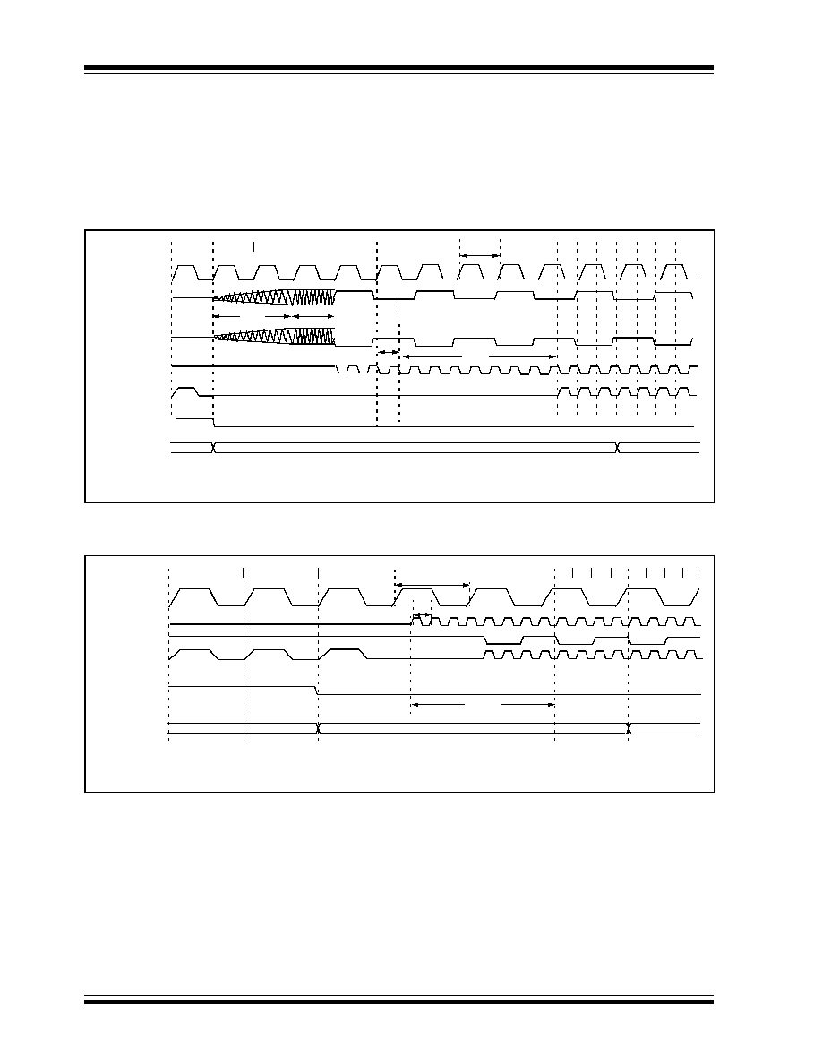
If the main oscillator is configured for HS4 (PLL) mode,
an oscillator start-up time (T
OST
) plus an additional PLL
time-out (T
PLL
) will occur. The PLL time-out is typically
2 ms and allows the PLL to lock to the main oscillator
frequency. A timing diagram indicating the transition
from the Timer1 oscillator to the main oscillator for HS4
mode is shown in Figure 2-9.
If the main oscillator is configured in the RC, RCIO, EC
or ECIO modes, there is no oscillator start-up time-out.
Operation will resume after eight cycles of the main
oscillator have been counted. A timing diagram indicat-
ing the transition from the Timer1 oscillator to the main
oscillator for RC, RCIO, EC and ECIO modes is shown
in Figure 2-10.
FIGURE 2-9:
TIMING FOR TRANSITION BETWEEN TIMER1 AND OSC1 (HS WITH PLL)
FIGURE 2-10:
TIMING FOR TRANSITION BETWEEN TIMER1 AND OSC1 (RC, EC)
Q4
Q1
Q1 Q2 Q3 Q4
Q1 Q2
OSC1
Internal System
SCS
(OSCCON<0>)
Program
PC
PC + 2
Note 1: T
OST
= 1024 T
OSC
(drawing not to scale).
T1OSI
Clock
T
OST
Q3
PC + 4
T
PLL
T
OSC
T
T
1
P
T
SCS
Q4
OSC2
PLL Clock
Input
1
2
3
4
5
6
7
8
Counter
Q3
Q4
Q1
Q1 Q2 Q3 Q4 Q1 Q2 Q3
OSC1
Internal System
SCS
(OSCCON<0>)
Program
PC
PC + 2
Note 1: RC Oscillator mode assumed.
PC + 4
T1OSI
Clock
OSC2
Q4
T
T
1
P
T
OSC
T
SCS
1
2
3
4
5
6
7
8
Counter

2002 Microchip Technology Inc.
Preliminary
DS41159B-page 23
PIC18FXX8
2.7
Effects of SLEEP Mode on the
On-Chip Oscillator
When the device executes a
SLEEP
instruction, the
on-chip clocks and oscillator are turned off and the
device is held at the beginning of an instruction cycle
(Q1 state). With the oscillator off, the OSC1 and OSC2
signals will stop oscillating. Since all the transistor
switching currents have been removed, SLEEP mode
achieves the lowest current consumption of the device
(only leakage currents). Enabling any on-chip feature
that will operate during SLEEP will increase the current
consumed during SLEEP. The user can wake from
SLEEP through external RESET, Watchdog Timer
Reset, or through an interrupt.
2.8
Power-up Delays
Power-up delays are controlled by two timers, so that
no external RESET circuitry is required for most appli-
cations. The delays ensure that the device is kept in
RESET until the device power supply and clock are sta-
ble. For additional information on RESET operation,
see Section 3.0.
The first timer is the Power-up Timer (PWRT), which
optionally provides a fixed delay of T
PWRT
(parameter
#D033) on power-up only (POR and BOR). The second
timer is the Oscillator Start-up Timer (OST), intended to
keep the chip in RESET until the crystal oscillator is
stable.
With the PLL enabled (HS4 Oscillator mode), the time-
out sequence following a Power-on Reset is different
from other Oscillator modes. The time-out sequence is
as follows: the PWRT time-out is invoked after a POR
time delay has expired, then the Oscillator Start-up
Timer (OST) is invoked. However, this is still not a suf-
ficient amount of time to allow the PLL to lock at high
frequencies. The PWRT timer is used to provide an
additional time-out. This time is called T
PLL
(parameter
#7) to allow the PLL ample time to lock to the incoming
clock frequency.
TABLE 2-3:
OSC1 AND OSC2 PIN STATES IN SLEEP MODE
OSC Mode
OSC1 Pin
OSC2 Pin
RC
Floating, external resistor should pull high
At logic low
RCIO
Floating, external resistor should pull high
Configured as PORTA, bit 6
ECIO
Floating
Configured as PORTA, bit 6
EC
Floating
At logic low
LP, XT, and HS
Feedback inverter disabled, at quiescent
voltage level
Feedback inverter disabled, at quiescent
voltage level
Note:
See Table 3-1 in Section 3.0, for time-outs due to SLEEP and MCLR Reset.

PIC18FXX8
DS41159B-page 24
Preliminary
2002 Microchip Technology Inc.
NOTES:
2002 Microchip Technology Inc.
Preliminary
DS41159B-page 25
PIC18FXX8
3.0
RESET
The PIC18FXX8 differentiates between various kinds
of RESET:
a)
Power-on Reset (POR)
b)
MCLR Reset during normal operation
c)
MCLR Reset during SLEEP
d)
Watchdog Timer (WDT) Reset during normal
operation
e)
Programmable Brown-out Reset (PBOR)
f)
RESET
Instruction
g)
Stack Full Reset
h)
Stack Underflow Reset
Most registers are unaffected by a RESET. Their status
is unknown on POR and unchanged by all other
RESETS. The other registers are forced to a "RESET"
state on Power-on Reset, MCLR, WDT Reset, Brown-
out Reset, MCLR Reset during SLEEP and by the
RESET
instruction.
Most registers are not affected by a WDT wake-up,
since this is viewed as the resumption of normal oper-
ation. Status bits from the RCON register, RI, TO, PD,
POR and BOR are set or cleared differently in different
RESET situations, as indicated in Table 3-2. These bits
are used in software to determine the nature of the
RESET. See Table 3-3 for a full description of the
RESET states of all registers.
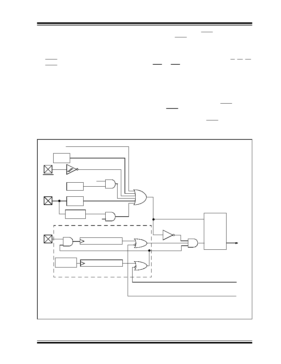
A simplified block diagram of the on-chip RESET circuit
is shown in Figure 3-1.
The Enhanced MCU devices have a MCLR noise filter
in the MCLR Reset path. The filter will detect and
ignore small pulses.
A WDT Reset does not drive MCLR pin low.
FIGURE 3-1:
SIMPLIFIED BLOCK DIAGRAM OF ON-CHIP RESET CIRCUIT
S
R
Q
External Reset
MCLR
V
DD
OSC1
V
DD
Rise
Detect
OST/PWRT
On-chip
RC OSC
(1)
WDT
Time-out
Power-on Reset
OST
10-bit Ripple Counter
PWRT
Chip_Reset
10-bit Ripple Counter
Reset
Enable OST
(2)
Enable PWRT
SLEEP
Note
1:
This is a separate oscillator from the RC oscillator of the CLKI pin.
2: See Table 3-1 for time-out situations.
Brown-out
Reset
BOREN
RESET
Instruction
Stack
Pointer
Stack Full/Underflow Reset
WDT
Module
PIC18FXX8
DS41159B-page 26
Preliminary
2002 Microchip Technology Inc.
3.1
Power-on Reset (POR)
A Power-on Reset pulse is generated on-chip when a
V
DD
rise is detected. To take advantage of the POR cir-
cuitry, connect the MCLR pin directly (or through a
resistor) to V
DD
. This eliminates external RC compo-
nents usually needed to create a Power-on Reset
delay. A minimum rise rate for V
DD
is specified (refer to
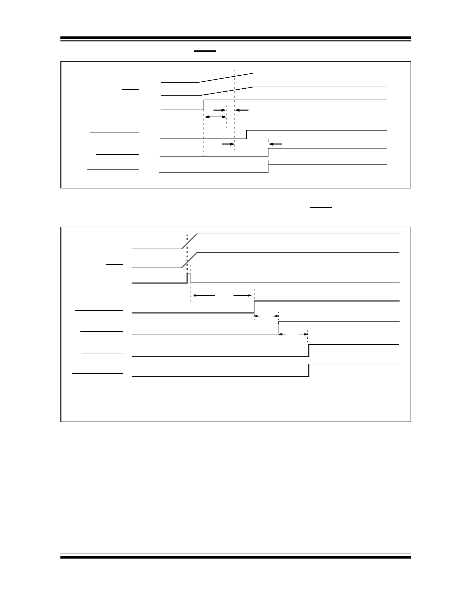
parameter D004). For a slow rise time, see Figure 3-2.
When the device starts normal operation (exits the
RESET condition), device operating parameters (volt-
age, frequency, temperature, etc.) must be met to
ensure operation. If these conditions are not met, the
device must be held in RESET until the operating con-
ditions are met. Brown-out Reset may be used to meet
the voltage start-up condition.
3.2
MCLR
PIC18FXX8 devices have a noise filter in the MCLR
Reset path. The filter will detect and ignore small
pulses.
It should be noted that a WDT Reset does not drive
MCLR pin low.
The behavior of the ESD protection on the MCLR pin
differs from previous devices of this family. Voltages
applied to the pin that exceed its specification can
result in both resets and current draws outside of
device specification during the RESET event. For this
reason, Microchip recommends that the MCLR pin no
longer be tied directly to V
DD
. The use of an RC
network, as shown in Figure 3-2, is suggested.
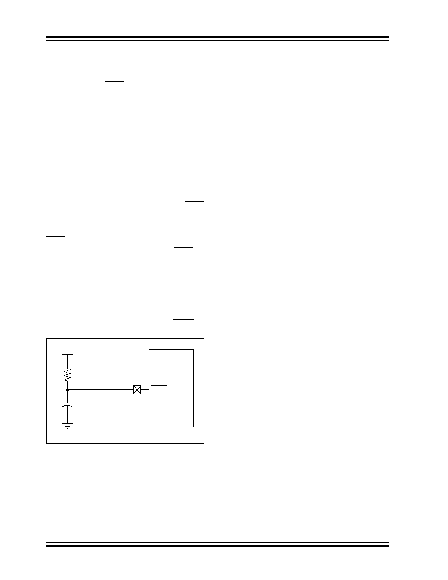
FIGURE 3-2:
RECOMMENDED MCLR
CIRCUIT
3.3
Power-up Timer (PWRT)
The Power-up Timer provides a fixed nominal time-out
(parameter #33), only on power-up from the POR. The
Power-up Timer operates on an internal RC oscillator.
The chip is kept in RESET as long as the PWRT is
active. The PWRT's time delay allows V
DD
to rise to an
acceptable level. A configuration bit (PWRTEN in
CONFIG2L register) is provided to enable/disable the
PWRT.
The power-up time delay will vary from chip to chip due
to V
DD
, temperature and process variation. See DC
parameter #33 for details.
3.4
Oscillator Start-up Timer (OST)
The Oscillator Start-up Timer (OST) provides 1024
oscillator cycle (from OSC1 input) delay after the
PWRT delay is over (parameter #32). This additional
delay ensures that the crystal oscillator or resonator
has started and stabilized.
The OST time-out is invoked only for XT, LP, HS and
HS4 modes and only on Power-on Reset or wake-up
from SLEEP.
3.5
PLL Lock Time-out
With the PLL enabled, the time-out sequence following
a Power-on Reset is different from other oscillator
modes. A portion of the Power-up Timer is used to pro-
vide a fixed time-out that is sufficient for the PLL to lock
to the main oscillator frequency. This PLL lock time-out
(T
PLL
) is typically 2 ms and follows the oscillator
start-up time-out (OST).
3.6
Brown-out Reset (BOR)
A configuration bit, BOREN, can disable (if clear/
programmed), or enable (if set), the Brown-out Reset
circuitry. If V
DD
falls below parameter D005 for greater
than parameter #35, the brown-out situation resets the
chip. A RESET may not occur if V
DD
falls below param-
eter D005 for less than parameter #35. The chip will
remain in Brown-out Reset until V
DD
rises above BV
DD
.
The Power-up Timer will then be invoked and will keep
the chip in RESET an additional time delay (parameter
#33). If V
DD
drops below BV
DD
while the Power-up
Timer is running, the chip will go back into a Brown-out
Reset and the Power-up Timer will be initialized. Once
V
DD
rises above BV
DD
, the Power-up Timer will
execute the additional time delay.
C1
0.1
�
F
R1
1 k
(or greater)
(not critical)
V
DD
MCLR
PIC18FXX8
2002 Microchip Technology Inc.
Preliminary
DS41159B-page 27
PIC18FXX8
3.7
Time-out Sequence
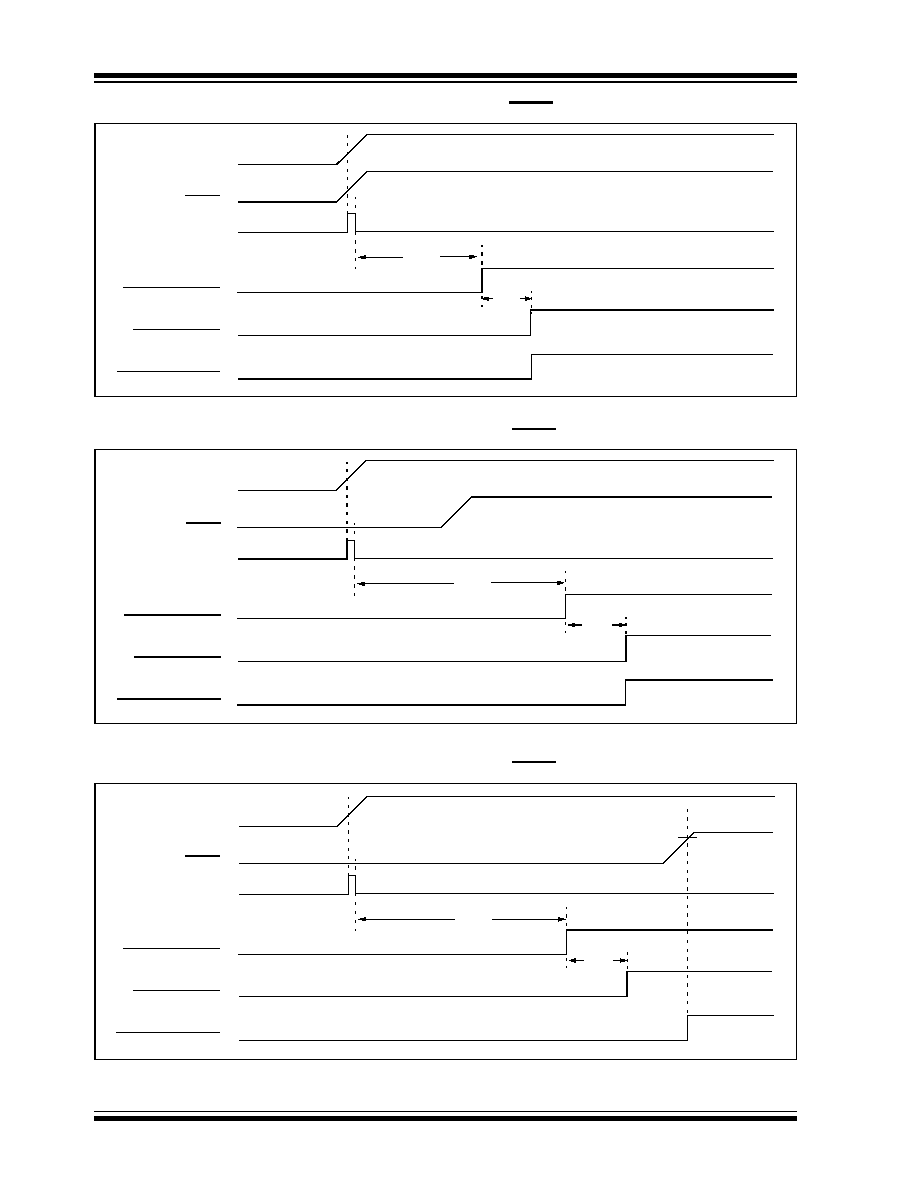
On power-up, the time-out sequence is as follows:
First, PWRT time-out is invoked after the POR time
delay has expired, then OST is activated. The total
time-out will vary based on oscillator configuration and
the status of the PWRT. For example, in RC mode with
the PWRT disabled, there will be no time-out at all.
Figure 3-3, Figure 3-4, Figure 3-5, Figure 3-6 and
Figure 3-7 depict time-out sequences on power-up.
Since the time-outs occur from the POR pulse, if MCLR
is kept low long enough, the time-outs will expire.
Bringing MCLR high will begin execution immediately
(Figure 3-5). This is useful for testing purposes or to
synchronize more than one PIC18FXX8 device
operating in parallel.
Table 3-2 shows the RESET conditions for some
Special Function Registers, while Table 3-3 shows the
RESET conditions for all registers.
TABLE 3-1:
TIME-OUT IN VARIOUS SITUATIONS
REGISTER 3-1:
RCON REGISTER BITS AND POSITIONS
TABLE 3-2:
STATUS BITS, THEIR SIGNIFICANCE AND THE INITIALIZATION CONDITION FOR
RCON REGISTER
Oscillator
Configuration
Power-up
(2)
Brown-out
(2)
Wake-up from
SLEEP or
Oscillator Switch
PWRTEN = 0
PWRTEN = 1
HS with PLL enabled
(1)
72 ms + 1024 T
OSC
+ 2 ms 1024 T
OSC
+ 2 ms 72 ms + 1024 T
OSC
+ 2 ms 1024 T
OSC
+ 2 ms
HS, XT, LP
72 ms + 1024 T
OSC
1024 T
OSC
72 ms + 1024 T
OSC
1024 T
OSC
EC
72 ms
--
72 ms
--
External RC
72 ms
--
72 ms
--
Note 1: 2 ms = Nominal time required for the 4X PLL to lock.
2: 72 ms is the nominal power-up timer delay.
R/W-0
U-0
U-0
R/W-1
R/W-1
R/W-1
R/W-1
R/W-1
IPEN
--
--
RI
TO
PD
POR
BOR
bit 7
bit 0
Condition
Program
Counter
RCON
Register
RI
TO
PD
POR
BOR
STKFUL
STKUNF
Power-on Reset
0000h
0--1 1100
1
1
1
0
0
u
u
MCLR Reset during normal
operation
0000h
0--u uuuu
u
u
u
u
u
u
u
Software Reset during normal
operation
0000h
0--0 uuuu
0
u
u
u
u
u
u
Stack Full Reset during normal
operation
0000h
0--u uu11
u
u
u
1
1
u
1
Stack Underflow Reset during
normal operation
0000h
0--u uu11
u
u
u
1
1
1
u
MCLR Reset during SLEEP
0000h
0--u 10uu
u
1
0
u
u
u
u
WDT Reset
0000h
0--u 01uu
u
0
1
u
u
u
u
WDT Wake-up
PC + 2
u--u 00uu
u
0
0
u
u
u
u
Brown-out Reset
0000h
0--1 11u0
1
1
1
u
0
u
u
Interrupt Wake-up from SLEEP
PC + 2
(1)
u--u 00uu
u
0
0
u
u
u
u
Legend:
u
= unchanged,
x
= unknown, - = unimplemented bit, read as '0'
Note 1: When the wake-up is due to an interrupt and the GIEH or GIEL bits are set, the PC is loaded with the
interrupt vector (
0x000008h
or
0x000018h
).
PIC18FXX8
DS41159B-page 28
Preliminary
2002 Microchip Technology Inc.
FIGURE 3-3:
TIME-OUT SEQUENCE ON POWER-UP (MCLR TIED TO V
DD
VIA RC NETWORK)
FIGURE 3-4:
TIME-OUT SEQUENCE ON POWER-UP (MCLR NOT TIED TO V
DD
): CASE 1
FIGURE 3-5:
TIME-OUT SEQUENCE ON POWER-UP (MCLR NOT TIED TO V
DD
): CASE 2
T
PWRT
T
OST
V
DD
MCLR
INTERNAL POR
PWRT TIME-OUT
OST TIME-OUT
INTERNAL RESET
T
PWRT
T
OST
V
DD
MCLR
INTERNAL POR
PWRT TIME-OUT
OST TIME-OUT
INTERNAL RESET
V
DD
MCLR
INTERNAL POR
PWRT TIME-OUT
OST TIME-OUT
INTERNAL RESET
T
PWRT
T
OST
2002 Microchip Technology Inc.
Preliminary
DS41159B-page 29
PIC18FXX8
FIGURE 3-6:
SLOW RISE TIME (MCLR TIED TO V
DD
VIA RC NETWORK)
FIGURE 3-7:
TIME-OUT SEQUENCE ON POR W/ PLL ENABLED (MCLR TIED TO V
DD
VIA RC NETWORK)
V
DD
MCLR
INTERNAL POR
PWRT TIME-OUT
OST TIME-OUT
INTERNAL RESET
1V
5V
T
PWRT
T
OST
T
DEADTIME
0V
T
PWRT
T
OST
V
DD
MCLR
INTERNAL POR
PWRT TIME-OUT
OST TIME-OUT
INTERNAL RESET
PLL TIME-OUT
T
PLL
T
OST
= 1024 clock cycles.
T
PLL
2 ms max. First three stages of the PWRT timer.

PIC18FXX8
DS41159B-page 30
Preliminary
2002 Microchip Technology Inc.
TABLE 3-3:
INITIALIZATION CONDITIONS FOR ALL REGISTERS
Register
Applicable Devices
Power-on Reset,
Brown-out Reset
MCLR Reset
WDT Reset
RESET
Instruction
Stack Resets
Wake-up via WDT
or Interrupt
TOSU
PIC18F2X8 PIC18F4X8
---0 0000
---0 0000
---0 uuuu
(3)
TOSH
PIC18F2X8 PIC18F4X8
0000 0000
0000 0000
uuuu uuuu
(3)
TOSL
PIC18F2X8 PIC18F4X8
0000 0000
0000 0000
uuuu uuuu
(3)
STKPTR
PIC18F2X8 PIC18F4X8
00-0 0000
uu-0 0000
uu-u uuuu
(3)
PCLATU
PIC18F2X8 PIC18F4X8
---0 0000
---0 0000
---u uuuu
PCLATH
PIC18F2X8 PIC18F4X8
0000 0000
0000 0000
uuuu uuuu
PCL
PIC18F2X8 PIC18F4X8
0000 0000
0000 0000
PC + 2
(2)
TBLPTRU
PIC18F2X8 PIC18F4X8
--00 0000
--00 0000
--uu uuuu
TBLPTRH
PIC18F2X8 PIC18F4X8
0000 0000
0000 0000
uuuu uuuu
TBLPTRL
PIC18F2X8 PIC18F4X8
0000 0000
0000 0000
uuuu uuuu
TABLAT
PIC18F2X8 PIC18F4X8
0000 0000
0000 0000
uuuu uuuu
PRODH
PIC18F2X8 PIC18F4X8
xxxx xxxx
uuuu uuuu
uuuu uuuu
PRODL
PIC18F2X8 PIC18F4X8
xxxx xxxx
uuuu uuuu
uuuu uuuu
INTCON
PIC18F2X8 PIC18F4X8
0000 000x
0000 000u
uuuu uuuu
(1)
INTCON2
PIC18F2X8 PIC18F4X8
111- -1-1
111- -1-1
uuuu -u-u
(1)
INTCON3
PIC18F2X8 PIC18F4X8
11-- 0-00
11-- 0-00
uu-u u-uu
(1)
INDF0
PIC18F2X8 PIC18F4X8
N/A
N/A
N/A
POSTINC0
PIC18F2X8 PIC18F4X8
N/A
N/A
N/A
POSTDEC0
PIC18F2X8 PIC18F4X8
N/A
N/A
N/A
PREINC0
PIC18F2X8 PIC18F4X8
N/A
N/A
N/A
PLUSW0
PIC18F2X8 PIC18F4X8
N/A
N/A
N/A
FSR0H
PIC18F2X8 PIC18F4X8
---- 0000
---- 0000
---- uuuu
FSR0L
PIC18F2X8 PIC18F4X8
xxxx xxxx
uuuu uuuu
uuuu uuuu
WREG
PIC18F2X8 PIC18F4X8
xxxx xxxx
uuuu uuuu
uuuu uuuu
INDF1
PIC18F2X8 PIC18F4X8
N/A
N/A
N/A
POSTINC1
PIC18F2X8 PIC18F4X8
N/A
N/A
N/A
POSTDEC1
PIC18F2X8 PIC18F4X8
N/A
N/A
N/A
PREINC1
PIC18F2X8 PIC18F4X8
N/A
N/A
N/A
PLUSW1
PIC18F2X8 PIC18F4X8
N/A
N/A
N/A
Legend:
u
= unchanged,
x
= unknown,
-
= unimplemented bit, read as '0',
q
= value depends on condition.
Shaded cells indicate conditions do not apply for the designated device.
Note 1: One or more bits in the INTCONx or PIRx registers will be affected (to cause wake-up).
2: When the wake-up is due to an interrupt and the GIEL or GIEH bit is set, the PC is loaded with the interrupt
vector (
0008h
or
0018h
).
3: When the wake-up is due to an interrupt and the GIEL or GIEH bit is set, the TOSU, TOSH and TOSL are
updated with the current value of the PC. The STKPTR is modified to point to the next location in the
hardware stack.
4: See Table 3-2 for RESET value for specific condition.
5: Bit 6 of PORTA, LATA, and TRISA are enabled in ECIO and RCIO Oscillator modes only. In all other
Oscillator modes, they are disabled and read '0'.
6: Values for CANSTAT also apply to to its other instances (CANSTATRO1 through CANSTATRO4).

2002 Microchip Technology Inc.
Preliminary
DS41159B-page 31
PIC18FXX8
FSR1H
PIC18F2X8 PIC18F4X8
---- 0000
---- 0000
---- uuuu
FSR1L
PIC18F2X8 PIC18F4X8
xxxx xxxx
uuuu uuuu
uuuu uuuu
BSR
PIC18F2X8 PIC18F4X8
---- 0000
---- 0000
---- uuuu
INDF2
PIC18F2X8 PIC18F4X8
N/A
N/A
N/A
POSTINC2
PIC18F2X8 PIC18F4X8
N/A
N/A
N/A
POSTDEC2
PIC18F2X8 PIC18F4X8
N/A
N/A
N/A
PREINC2
PIC18F2X8 PIC18F4X8
N/A
N/A
N/A
PLUSW2
PIC18F2X8 PIC18F4X8
N/A
N/A
N/A
FSR2H
PIC18F2X8 PIC18F4X8
---- 0000
---- 0000
---- uuuu
FSR2L
PIC18F2X8 PIC18F4X8
xxxx xxxx
uuuu uuuu
uuuu uuuu
STATUS
PIC18F2X8 PIC18F4X8
---x xxxx
---u uuuu
---u uuuu
TMR0H
PIC18F2X8 PIC18F4X8
xxxx xxxx
uuuu uuuu
uuuu uuuu
TMR0L
PIC18F2X8 PIC18F4X8
xxxx xxxx
uuuu uuuu
uuuu uuuu
T0CON
PIC18F2X8 PIC18F4X8
1111 1111
1111 1111
uuuu uuuu
OSCCON
PIC18F2X8 PIC18F4X8
---- ---0
---- ---0
---- ---u
LVDCON
PIC18F2X8 PIC18F4X8
--00 0101
--00 0101
--uu uuuu
WDTCON
PIC18F2X8 PIC18F4X8
---- ---0
---- ---0
---- ---u
RCON
(4)
PIC18F2X8 PIC18F4X8
0--1 11q0
0--1 qquu
u--u qquu
TMR1H
PIC18F2X8 PIC18F4X8
xxxx xxxx
uuuu uuuu
uuuu uuuu
TMR1L
PIC18F2X8 PIC18F4X8
xxxx xxxx
uuuu uuuu
uuuu uuuu
T1CON
PIC18F2X8 PIC18F4X8
0-00 0000
u-uu uuuu
u-uu uuuu
TMR2
PIC18F2X8 PIC18F4X8
xxxx xxxx
uuuu uuuu
uuuu uuuu
PR2
PIC18F2X8 PIC18F4X8
1111 1111
1111 1111
1111 1111
T2CON
PIC18F2X8 PIC18F4X8
-000 0000
-000 0000
-uuu uuuu
SSPBUF
PIC18F2X8 PIC18F4X8
xxxx xxxx
uuuu uuuu
uuuu uuuu
SSPADD
PIC18F2X8 PIC18F4X8
0000 0000
0000 0000
uuuu uuuu
SSPSTAT
PIC18F2X8 PIC18F4X8
0000 0000
0000 0000
uuuu uuuu
SSPCON1
PIC18F2X8 PIC18F4X8
0000 0000
0000 0000
uuuu uuuu
SSPCON2
PIC18F2X8 PIC18F4X8
0000 0000
0000 0000
uuuu uuuu
TABLE 3-3:
INITIALIZATION CONDITIONS FOR ALL REGISTERS (CONTINUED)
Register
Applicable Devices
Power-on Reset,
Brown-out Reset
MCLR Reset
WDT Reset
RESET
Instruction
Stack Resets
Wake-up via WDT
or Interrupt
Legend:
u
= unchanged,
x
= unknown,
-
= unimplemented bit, read as '0',
q
= value depends on condition.
Shaded cells indicate conditions do not apply for the designated device.
Note 1: One or more bits in the INTCONx or PIRx registers will be affected (to cause wake-up).
2: When the wake-up is due to an interrupt and the GIEL or GIEH bit is set, the PC is loaded with the interrupt
vector (
0008h
or
0018h
).
3: When the wake-up is due to an interrupt and the GIEL or GIEH bit is set, the TOSU, TOSH and TOSL are
updated with the current value of the PC. The STKPTR is modified to point to the next location in the
hardware stack.
4: See Table 3-2 for RESET value for specific condition.
5: Bit 6 of PORTA, LATA, and TRISA are enabled in ECIO and RCIO Oscillator modes only. In all other
Oscillator modes, they are disabled and read '0'.
6: Values for CANSTAT also apply to to its other instances (CANSTATRO1 through CANSTATRO4).

PIC18FXX8
DS41159B-page 32
Preliminary
2002 Microchip Technology Inc.
ADRESH
PIC18F2X8 PIC18F4X8
xxxx xxxx
uuuu uuuu
uuuu uuuu
ADRESL
PIC18F2X8 PIC18F4X8
xxxx xxxx
uuuu uuuu
uuuu uuuu
ADCON0
PIC18F2X8 PIC18F4X8
0000 00-0
0000 00-0
uuuu uu-u
ADCON1
PIC18F2X8 PIC18F4X8
00-- 0000
00-- 0000
uu-- uuuu
CCPR1H
PIC18F2X8 PIC18F4X8
xxxx xxxx
uuuu uuuu
uuuu uuuu
CCPR1L
PIC18F2X8 PIC18F4X8
xxxx xxxx
uuuu uuuu
uuuu uuuu
CCP1CON
PIC18F2X8 PIC18F4X8
--00 0000
--00 0000
--uu uuuu
ECCPR1H
PIC18F2X8 PIC18F4X8
xxxx xxxx
uuuu uuuu
uuuu uuuu
ECCPR1L
PIC18F2X8 PIC18F4X8
xxxx xxxx
uuuu uuuu
uuuu uuuu
ECCP1CON
PIC18F2X8 PIC18F4X8
0000 0000
0000 0000
0000 0000
ECCP1DEL
PIC18F2X8 PIC18F4X8
0000 0000
0000 0000
0000 0000
ECCPAS
PIC18F2X8 PIC18F4X8
0000 0000
0000 0000
0000 0000
CVRCON
PIC18F2X8 PIC18F4X8
0000 0000
0000 0000
uuuu uuuu
CMCON
PIC18F2X8 PIC18F4X8
0000 0000
0000 0000
uuuu uuuu
TMR3H
PIC18F2X8 PIC18F4X8
xxxx xxxx
uuuu uuuu
uuuu uuuu
TMR3L
PIC18F2X8 PIC18F4X8
xxxx xxxx
uuuu uuuu
uuuu uuuu
T3CON
PIC18F2X8 PIC18F4X8
0000 0000
uuuu uuuu
uuuu uuuu
SPBRG
PIC18F2X8 PIC18F4X8
xxxx xxxx
uuuu uuuu
uuuu uuuu
RCREG
PIC18F2X8 PIC18F4X8
xxxx xxxx
uuuu uuuu
uuuu uuuu
TXREG
PIC18F2X8 PIC18F4X8
xxxx xxxx
uuuu uuuu
uuuu uuuu
TXSTA
PIC18F2X8 PIC18F4X8
0000 -01x
0000 -01u
uuuu -uuu
RCSTA
PIC18F2X8 PIC18F4X8
0000 000x
0000 000u
uuuu uuuu
EEADR
PIC18F2X8 PIC18F4X8
xxxx xxxx
uuuu uuuu
uuuu uuuu
EEDATA
PIC18F2X8 PIC18F4X8
xxxx xxxx
uuuu uuuu
uuuu uuuu
EECON2
PIC18F2X8 PIC18F4X8
xxxx xxxx
uuuu uuuu
uuuu uuuu
EECON1
PIC18F2X8 PIC18F4X8
xx-0 x000
uu-0 u000
uu-0 u000
IPR3
PIC18F2X8 PIC18F4X8
1111 1111
1111 1111
uuuu uuuu
PIR3
PIC18F2X8 PIC18F4X8
0000 0000
0000 0000
uuuu uuuu
PIE3
PIC18F2X8 PIC18F4X8
0000 0000
0000 0000
uuuu uuuu
TABLE 3-3:
INITIALIZATION CONDITIONS FOR ALL REGISTERS (CONTINUED)
Register
Applicable Devices
Power-on Reset,
Brown-out Reset
MCLR Reset
WDT Reset
RESET
Instruction
Stack Resets
Wake-up via WDT
or Interrupt
Legend:
u
= unchanged,
x
= unknown,
-
= unimplemented bit, read as '0',
q
= value depends on condition.
Shaded cells indicate conditions do not apply for the designated device.
Note 1: One or more bits in the INTCONx or PIRx registers will be affected (to cause wake-up).
2: When the wake-up is due to an interrupt and the GIEL or GIEH bit is set, the PC is loaded with the interrupt
vector (
0008h
or
0018h
).
3: When the wake-up is due to an interrupt and the GIEL or GIEH bit is set, the TOSU, TOSH and TOSL are
updated with the current value of the PC. The STKPTR is modified to point to the next location in the
hardware stack.
4: See Table 3-2 for RESET value for specific condition.
5: Bit 6 of PORTA, LATA, and TRISA are enabled in ECIO and RCIO Oscillator modes only. In all other
Oscillator modes, they are disabled and read '0'.
6: Values for CANSTAT also apply to to its other instances (CANSTATRO1 through CANSTATRO4).
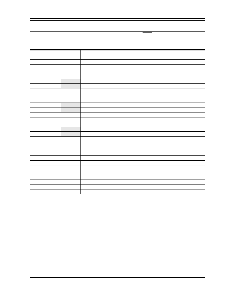
2002 Microchip Technology Inc.
Preliminary
DS41159B-page 33
PIC18FXX8
IPR2
PIC18F2X8 PIC18F4X8
-1-1 1111
-1-1 1111
-u-u uuuu
PIR2
PIC18F2X8 PIC18F4X8
-0-0 0000
-0-0 0000
-u-u uuuu
(1)
PIE2
PIC18F2X8 PIC18F4X8
-0-0 0000
-0-0 0000
-u-u uuuu
IPR1
PIC18F2X8 PIC18F4X8
1111 1111
1111 1111
uuuu uuuu
PIR1
PIC18F2X8 PIC18F4X8
0000 0000
0000 0000
uuuu uuuu
(1)
PIE1
PIC18F2X8 PIC18F4X8
0000 0000
0000 0000
uuuu uuuu
TRISE
PIC18F2X8 PIC18F4X8
0000 -111
0000 -111
uuuu -uuu
TRISD
PIC18F2X8 PIC18F4X8
1111 1111
1111 1111
uuuu uuuu
TRISC
PIC18F2X8 PIC18F4X8
1111 1111
1111 1111
uuuu uuuu
TRISB
PIC18F2X8 PIC18F4X8
1111 1111
1111 1111
uuuu uuuu
TRISA
(5)
PIC18F2X8 PIC18F4X8
-111 1111
(5)
-111 1111
(5)
-uuu uuuu
(5)
LATE
PIC18F2X8 PIC18F4X8
---- -xxx
---- -uuu
---- -uuu
LATD
PIC18F2X8 PIC18F4X8
xxxx xxxx
uuuu uuuu
uuuu uuuu
LATC
PIC18F2X8 PIC18F4X8
xxxx xxxx
uuuu uuuu
uuuu uuuu
LATB
PIC18F2X8 PIC18F4X8
xxxx xxxx
uuuu uuuu
uuuu uuuu
LATA
(5)
PIC18F2X8 PIC18F4X8
-xxx xxxx
(5)
-uuu uuuu
(5)
-uuu uuuu
(5)
PORTE
PIC18F2X8 PIC18F4X8
---- -xxx
---- -000
---- -uuu
PORTD
PIC18F2X8 PIC18F4X8
xxxx xxxx
uuuu uuuu
uuuu uuuu
PORTC
PIC18F2X8 PIC18F4X8
xxxx xxxx
uuuu uuuu
uuuu uuuu
PORTB
PIC18F2X8 PIC18F4X8
xxxx xxxx
uuuu uuuu
uuuu uuuu
PORTA
(5)
PIC18F2X8 PIC18F4X8
-x0x 0000
(5)
-u0u 0000
(5)
-uuu uuuu
(5)
TXERRCNT
PIC18F2X8 PIC18F4X8
0000 0000
0000 0000
uuuu uuuu
RXERRCNT
PIC18F2X8 PIC18F4X8
0000 0000
0000 0000
uuuu uuuu
COMSTAT
PIC18F2X8 PIC18F4X8
0000 0000
0000 0000
uuuu uuuu
CIOCON
PIC18F2X8 PIC18F4X8
1000 ----
1000 ----
uuuu ----
BRGCON3
PIC18F2X8 PIC18F4X8
-0-- -000
-0-- -000
-u-- -uuu
BRGCON2
PIC18F2X8 PIC18F4X8
0000 0000
0000 0000
uuuu uuuu
BRGCON1
PIC18F2X8 PIC18F4X8
0000 0000
0000 0000
uuuu uuuu
CANCON
PIC18F2X8 PIC18F4X8
xxxx xxx-
uuuu uuu-
uuuu uuu-
CANSTAT
(6)
PIC18F2X8 PIC18F4X8
xxx- xxx-
uuu- uuu-
uuu- uuu-
TABLE 3-3:
INITIALIZATION CONDITIONS FOR ALL REGISTERS (CONTINUED)
Register
Applicable Devices
Power-on Reset,
Brown-out Reset
MCLR Reset
WDT Reset
RESET
Instruction
Stack Resets
Wake-up via WDT
or Interrupt
Legend:
u
= unchanged,
x
= unknown,
-
= unimplemented bit, read as '0',
q
= value depends on condition.
Shaded cells indicate conditions do not apply for the designated device.
Note 1: One or more bits in the INTCONx or PIRx registers will be affected (to cause wake-up).
2: When the wake-up is due to an interrupt and the GIEL or GIEH bit is set, the PC is loaded with the interrupt
vector (
0008h
or
0018h
).
3: When the wake-up is due to an interrupt and the GIEL or GIEH bit is set, the TOSU, TOSH and TOSL are
updated with the current value of the PC. The STKPTR is modified to point to the next location in the
hardware stack.
4: See Table 3-2 for RESET value for specific condition.
5: Bit 6 of PORTA, LATA, and TRISA are enabled in ECIO and RCIO Oscillator modes only. In all other
Oscillator modes, they are disabled and read '0'.
6: Values for CANSTAT also apply to to its other instances (CANSTATRO1 through CANSTATRO4).

PIC18FXX8
DS41159B-page 34
Preliminary
2002 Microchip Technology Inc.
RXB0D7
PIC18F2X8 PIC18F4X8
xxxx xxxx
uuuu uuuu
uuuu uuuu
RXB0D6
PIC18F2X8 PIC18F4X8
xxxx xxxx
uuuu uuuu
uuuu uuuu
RXB0D5
PIC18F2X8 PIC18F4X8
xxxx xxxx
uuuu uuuu
uuuu uuuu
RXB0D4
PIC18F2X8 PIC18F4X8
xxxx xxxx
uuuu uuuu
uuuu uuuu
RXB0D3
PIC18F2X8 PIC18F4X8
xxxx xxxx
uuuu uuuu
uuuu uuuu
RXB0D2
PIC18F2X8 PIC18F4X8
xxxx xxxx
uuuu uuuu
uuuu uuuu
RXB0D1
PIC18F2X8 PIC18F4X8
xxxx xxxx
uuuu uuuu
uuuu uuuu
RXB0D0
PIC18F2X8 PIC18F4X8
xxxx xxxx
uuuu uuuu
uuuu uuuu
RXB0DLC
PIC18F2X8 PIC18F4X8
0xxx xxxx
0uuu uuuu
uuuu uuuu
RXB0EIDL
PIC18F2X8 PIC18F4X8
xxxx xxxx
uuuu uuuu
uuuu uuuu
RXB0EIDH
PIC18F2X8 PIC18F4X8
xxxx xxxx
uuuu uuuu
uuuu uuuu
RXB0SIDL
PIC18F2X8 PIC18F4X8
xxxx x-xx
uuuu u-uu
uuuu u-uu
RXB0SIDH
PIC18F2X8 PIC18F4X8
xxxx xxxx
uuuu uuuu
uuuu uuuu
RXB0CON
PIC18F2X8 PIC18F4X8
000- 0000
000- 0000
uuu- uuuu
RXB1D7
PIC18F2X8 PIC18F4X8
xxxx xxxx
uuuu uuuu
uuuu uuuu
RXB1D6
PIC18F2X8 PIC18F4X8
xxxx xxxx
uuuu uuuu
uuuu uuuu
RXB1D5
PIC18F2X8 PIC18F4X8
xxxx xxxx
uuuu uuuu
uuuu uuuu
RXB1D4
PIC18F2X8 PIC18F4X8
xxxx xxxx
uuuu uuuu
uuuu uuuu
RXB1D3
PIC18F2X8 PIC18F4X8
xxxx xxxx
uuuu uuuu
uuuu uuuu
RXB1D2
PIC18F2X8 PIC18F4X8
xxxx xxxx
uuuu uuuu
uuuu uuuu
RXB1D1
PIC18F2X8 PIC18F4X8
xxxx xxxx
uuuu uuuu
uuuu uuuu
RXB1D0
PIC18F2X8 PIC18F4X8
xxxx xxxx
uuuu uuuu
uuuu uuuu
RXB1DLC
PIC18F2X8 PIC18F4X8
0xxx xxxx
0uuu uuuu
uuuu uuuu
RXB1EIDL
PIC18F2X8 PIC18F4X8
xxxx xxxx
uuuu uuuu
uuuu uuuu
RXB1EIDH
PIC18F2X8 PIC18F4X8
xxxx xxxx
uuuu uuuu
uuuu uuuu
RXB1SIDL
PIC18F2X8 PIC18F4X8
xxxx x0xx
uuuu u0uu
uuuu uuuu
RXB1SIDH
PIC18F2X8 PIC18F4X8
xxxx xxxx
uuuu uuuu
uuuu uuuu
RXB1CON
PIC18F2X8 PIC18F4X8
0000 0000
0000 0000
uuuu uuuu
TXB0D7
PIC18F2X8 PIC18F4X8
xxxx xxxx
uuuu uuuu
uuuu uuuu
TXB0D6
PIC18F2X8 PIC18F4X8
xxxx xxxx
uuuu uuuu
uuuu uuuu
TXB0D5
PIC18F2X8 PIC18F4X8
xxxx xxxx
uuuu uuuu
uuuu uuuu
TXB0D4
PIC18F2X8 PIC18F4X8
xxxx xxxx
uuuu uuuu
uuuu uuuu
TXB0D3
PIC18F2X8 PIC18F4X8
xxxx xxxx
uuuu uuuu
uuuu uuuu
TXB0D2
PIC18F2X8 PIC18F4X8
xxxx xxxx
uuuu uuuu
uuuu uuuu
TXB0D1
PIC18F2X8 PIC18F4X8
xxxx xxxx
uuuu uuuu
uuuu uuuu
TXB0D0
PIC18F2X8 PIC18F4X8
xxxx xxxx
uuuu uuuu
uuuu uuuu
TABLE 3-3:
INITIALIZATION CONDITIONS FOR ALL REGISTERS (CONTINUED)
Register
Applicable Devices
Power-on Reset,
Brown-out Reset
MCLR Reset
WDT Reset
RESET
Instruction
Stack Resets
Wake-up via WDT
or Interrupt
Legend:
u
= unchanged,
x
= unknown,
-
= unimplemented bit, read as '0',
q
= value depends on condition.
Shaded cells indicate conditions do not apply for the designated device.
Note 1: One or more bits in the INTCONx or PIRx registers will be affected (to cause wake-up).
2: When the wake-up is due to an interrupt and the GIEL or GIEH bit is set, the PC is loaded with the interrupt
vector (
0008h
or
0018h
).
3: When the wake-up is due to an interrupt and the GIEL or GIEH bit is set, the TOSU, TOSH and TOSL are
updated with the current value of the PC. The STKPTR is modified to point to the next location in the
hardware stack.
4: See Table 3-2 for RESET value for specific condition.
5: Bit 6 of PORTA, LATA, and TRISA are enabled in ECIO and RCIO Oscillator modes only. In all other
Oscillator modes, they are disabled and read '0'.
6: Values for CANSTAT also apply to to its other instances (CANSTATRO1 through CANSTATRO4).

2002 Microchip Technology Inc.
Preliminary
DS41159B-page 35
PIC18FXX8
TXB0DLC
PIC18F2X8 PIC18F4X8
0x00 xxxx
0u00 uuuu
uuuu uuuu
TXB0EIDL
PIC18F2X8 PIC18F4X8
xxxx xxxx
uuuu uuuu
uuuu uuuu
TXB0EIDH
PIC18F2X8 PIC18F4X8
xxxx xxxx
uuuu uuuu
uuuu uuuu
TXB0SIDL
PIC18F2X8 PIC18F4X8
xxx0 x0xx
uuu0 u0uu
uuuu uuuu
TXB0SIDH
PIC18F2X8 PIC18F4X8
xxxx xxxx
uuuu uuuu
uuuu uuuu
TXB0CON
PIC18F2X8 PIC18F4X8
0000 0000
0000 0000
uuuu uuuu
TXB1D7
PIC18F2X8 PIC18F4X8
xxxx xxxx
uuuu uuuu
uuuu uuuu
TXB1D6
PIC18F2X8 PIC18F4X8
xxxx xxxx
uuuu uuuu
uuuu uuuu
TXB1D5
PIC18F2X8 PIC18F4X8
xxxx xxxx
uuuu uuuu
uuuu uuuu
TXB1D4
PIC18F2X8 PIC18F4X8
xxxx xxxx
uuuu uuuu
uuuu uuuu
TXB1D3
PIC18F2X8 PIC18F4X8
xxxx xxxx
uuuu uuuu
uuuu uuuu
TXB1D2
PIC18F2X8 PIC18F4X8
xxxx xxxx
uuuu uuuu
uuuu uuuu
TXB1D1
PIC18F2X8 PIC18F4X8
xxxx xxxx
uuuu uuuu
uuuu uuuu
TXB1D0
PIC18F2X8 PIC18F4X8
xxxx xxxx
uuuu uuuu
uuuu uuuu
TXB1DLC
PIC18F2X8 PIC18F4X8
0x00 xxxx
0u00 uuuu
uuuu uuuu
TXB1EIDL
PIC18F2X8 PIC18F4X8
xxxx xxxx
uuuu uuuu
uuuu uuuu
TXB1EIDH
PIC18F2X8 PIC18F4X8
xxxx xxxx
uuuu uuuu
uuuu uuuu
TXB1SIDL
PIC18F2X8 PIC18F4X8
xxx0 x0xx
uuu0 u0uu
uuuu uuuu
TXB1SIDH
PIC18F2X8 PIC18F4X8
xxxx xxxx
uuuu uuuu
uuuu uuuu
TXB1CON
PIC18F2X8 PIC18F4X8
0000 0000
0000 0000
uuuu uuuu
TXB2D7
PIC18F2X8 PIC18F4X8
xxxx xxxx
uuuu uuuu
uuuu uuuu
TXB2D6
PIC18F2X8 PIC18F4X8
xxxx xxxx
uuuu uuuu
uuuu uuuu
TXB2D5
PIC18F2X8 PIC18F4X8
xxxx xxxx
uuuu uuuu
uuuu uuuu
TXB2D4
PIC18F2X8 PIC18F4X8
xxxx xxxx
uuuu uuuu
uuuu uuuu
TXB2D3
PIC18F2X8 PIC18F4X8
xxxx xxxx
uuuu uuuu
uuuu uuuu
TXB2D2
PIC18F2X8 PIC18F4X8
xxxx xxxx
uuuu uuuu
uuuu uuuu
TXB2D1
PIC18F2X8 PIC18F4X8
xxxx xxxx
uuuu uuuu
uuuu uuuu
TXB2D0
PIC18F2X8 PIC18F4X8
xxxx xxxx
uuuu uuuu
uuuu uuuu
TXB2DLC
PIC18F2X8 PIC18F4X8
0x00 xxxx
0u00 uuuu
uuuu uuuu
TXB2EIDL
PIC18F2X8 PIC18F4X8
xxxx xxxx
uuuu uuuu
uuuu uuuu
TXB2EIDH
PIC18F2X8 PIC18F4X8
xxxx xxxx
uuuu uuuu
uuuu uuuu
TXB2SIDL
PIC18F2X8 PIC18F4X8
xxx0 x0xx
uuu0 u0uu
uuuu uuuu
TXB2SIDH
PIC18F2X8 PIC18F4X8
xxxx xxxx
uuuu uuuu
uuuu uuuu
TXB2CON
PIC18F2X8 PIC18F4X8
0000 0000
0000 0000
uuuu uuuu
TABLE 3-3:
INITIALIZATION CONDITIONS FOR ALL REGISTERS (CONTINUED)
Register
Applicable Devices
Power-on Reset,
Brown-out Reset
MCLR Reset
WDT Reset
RESET
Instruction
Stack Resets
Wake-up via WDT
or Interrupt
Legend:
u
= unchanged,
x
= unknown,
-
= unimplemented bit, read as '0',
q
= value depends on condition.
Shaded cells indicate conditions do not apply for the designated device.
Note 1: One or more bits in the INTCONx or PIRx registers will be affected (to cause wake-up).
2: When the wake-up is due to an interrupt and the GIEL or GIEH bit is set, the PC is loaded with the interrupt
vector (
0008h
or
0018h
).
3: When the wake-up is due to an interrupt and the GIEL or GIEH bit is set, the TOSU, TOSH and TOSL are
updated with the current value of the PC. The STKPTR is modified to point to the next location in the
hardware stack.
4: See Table 3-2 for RESET value for specific condition.
5: Bit 6 of PORTA, LATA, and TRISA are enabled in ECIO and RCIO Oscillator modes only. In all other
Oscillator modes, they are disabled and read '0'.
6: Values for CANSTAT also apply to to its other instances (CANSTATRO1 through CANSTATRO4).

PIC18FXX8
DS41159B-page 36
Preliminary
2002 Microchip Technology Inc.
RXM1EIDL
PIC18F2X8 PIC18F4X8
xxxx xxxx
uuuu uuuu
uuuu uuuu
RXM1EIDH
PIC18F2X8 PIC18F4X8
xxxx xxxx
uuuu uuuu
uuuu uuuu
RXM1SIDL
PIC18F2X8 PIC18F4X8
xxx- --xx
uuu- --uu
uuu- --uu
RXM1SIDH
PIC18F2X8 PIC18F4X8
xxxx xxxx
uuuu uuuu
uuuu uuuu
RXM0EIDL
PIC18F2X8 PIC18F4X8
xxxx xxxx
uuuu uuuu
uuuu uuuu
RXM0EIDH
PIC18F2X8 PIC18F4X8
xxxx xxxx
uuuu uuuu
uuuu uuuu
RXM0SIDL
PIC18F2X8 PIC18F4X8
xxx- --xx
uuu- --uu
uuu- --uu
RXM0SIDH
PIC18F2X8 PIC18F4X8
xxxx xxxx
uuuu uuuu
uuuu uuuu
RXF5EIDL
PIC18F2X8 PIC18F4X8
xxxx xxxx
uuuu uuuu
uuuu uuuu
RXF5EIDH
PIC18F2X8 PIC18F4X8
xxxx xxxx
uuuu uuuu
uuuu uuuu
RXF5SIDL
PIC18F2X8 PIC18F4X8
xxx- x-xx
uuu- u-uu
uuu- u-uu
RXF5SIDH
PIC18F2X8 PIC18F4X8
xxxx xxxx
uuuu uuuu
uuuu uuuu
RXF4EIDL
PIC18F2X8 PIC18F4X8
xxxx xxxx
uuuu uuuu
uuuu uuuu
RXF4EIDH
PIC18F2X8 PIC18F4X8
xxxx xxxx
uuuu uuuu
uuuu uuuu
RXF4SIDL
PIC18F2X8 PIC18F4X8
xxx- x-xx
uuu- u-uu
uuu- u-uu
RXF4SIDH
PIC18F2X8 PIC18F4X8
xxxx xxxx
uuuu uuuu
uuuu uuuu
RXF3EIDL
PIC18F2X8 PIC18F4X8
xxxx xxxx
uuuu uuuu
uuuu uuuu
RXF3EIDH
PIC18F2X8 PIC18F4X8
xxxx xxxx
uuuu uuuu
uuuu uuuu
RXF3SIDL
PIC18F2X8 PIC18F4X8
xxx- x-xx
uuu- u-uu
uuu- u-uu
RXF3SIDH
PIC18F2X8 PIC18F4X8
xxxx xxxx
uuuu uuuu
uuuu uuuu
RXF2EIDL
PIC18F2X8 PIC18F4X8
xxxx xxxx
uuuu uuuu
uuuu uuuu
RXF2EIDH
PIC18F2X8 PIC18F4X8
xxxx xxxx
uuuu uuuu
uuuu uuuu
RXF2SIDL
PIC18F2X8 PIC18F4X8
xxx- x-xx
uuu- u-uu
uuu- u-uu
RXF2SIDH
PIC18F2X8 PIC18F4X8
xxxx xxxx
uuuu uuuu
uuuu uuuu
RXF1EIDL
PIC18F2X8 PIC18F4X8
xxxx xxxx
uuuu uuuu
uuuu uuuu
RXF1EIDH
PIC18F2X8 PIC18F4X8
xxxx xxxx
uuuu uuuu
uuuu uuuu
RXF1SIDL
PIC18F2X8 PIC18F4X8
xxx- x-xx
uuu- u-uu
uuu- u-uu
RXF1SIDH
PIC18F2X8 PIC18F4X8
xxxx xxxx
uuuu uuuu
uuuu uuuu
RXF0EIDL
PIC18F2X8 PIC18F4X8
xxxx xxxx
uuuu uuuu
uuuu uuuu
RXF0EIDH
PIC18F2X8 PIC18F4X8
xxxx xxxx
uuuu uuuu
uuuu uuuu
RXF0SIDL
PIC18F2X8 PIC18F4X8
xxx- x-xx
uuu- u-uu
uuu- u-uu
RXF0SIDH
PIC18F2X8 PIC18F4X8
xxxx xxxx
uuuu uuuu
uuuu uuuu
TABLE 3-3:
INITIALIZATION CONDITIONS FOR ALL REGISTERS (CONTINUED)
Register
Applicable Devices
Power-on Reset,
Brown-out Reset
MCLR Reset
WDT Reset
RESET
Instruction
Stack Resets
Wake-up via WDT
or Interrupt
Legend:
u
= unchanged,
x
= unknown,
-
= unimplemented bit, read as '0',
q
= value depends on condition.
Shaded cells indicate conditions do not apply for the designated device.
Note 1: One or more bits in the INTCONx or PIRx registers will be affected (to cause wake-up).
2: When the wake-up is due to an interrupt and the GIEL or GIEH bit is set, the PC is loaded with the interrupt
vector (
0008h
or
0018h
).
3: When the wake-up is due to an interrupt and the GIEL or GIEH bit is set, the TOSU, TOSH and TOSL are
updated with the current value of the PC. The STKPTR is modified to point to the next location in the
hardware stack.
4: See Table 3-2 for RESET value for specific condition.
5: Bit 6 of PORTA, LATA, and TRISA are enabled in ECIO and RCIO Oscillator modes only. In all other
Oscillator modes, they are disabled and read '0'.
6: Values for CANSTAT also apply to to its other instances (CANSTATRO1 through CANSTATRO4).
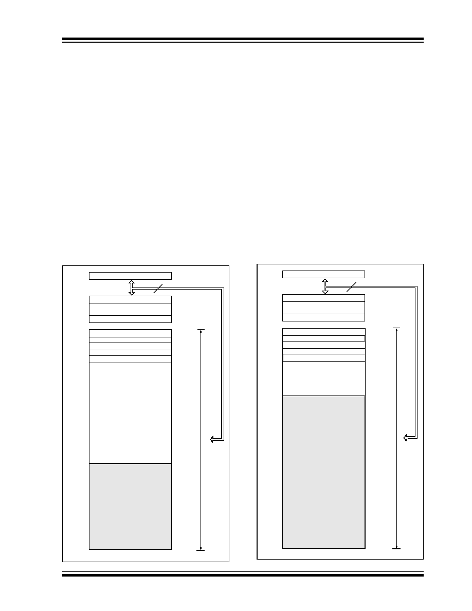
2002 Microchip Technology Inc.
Preliminary
DS41159B-page 37
PIC18FXX8
4.0
MEMORY ORGANIZATION
There are three memory blocks in Enhanced MCU
devices. These memory blocks are:
� Enhanced FLASH Program Memory
� Data Memory
� EEPROM Data Memory
Data and program memory use separate busses,
which allows concurrent access of these blocks. Addi-
tional detailed information on Data EEPROM and
FLASH program memory is provided in Section 5.0 and
Section 6.0, respectively.
4.1
Program Memory Organization
The PIC18F258/458 devices have a 21-bit program
counter that is capable of addressing a 2 Mbyte
program memory space.
The RESET vector address is at 0000h and the
interrupt vector addresses are at 0008h and 0018h.
FIGURE 4-1:
PROGRAM MEMORY MAP
AND STACK FOR
PIC18F258/458
Figure 4-1 shows the diagram for program memory
map and stack for the PIC18F258 and PIC18F458.
Figure 4-2 shows the the diagram for the program
memory map and stack for the PIC18F248 and
PIC18F448.
4.1.1
INTERNAL PROGRAM MEMORY
OPERATION
The PIC18F258 and the PIC18F458 have 32 Kbytes of
internal Enhanced FLASH program memory. This
means that the PIC18F258 and the PIC18F458 can
store up to 16K of single word instructions. The
PIC18F248 and PIC18F448 have 16 Kbytes of
Enhanced FLASH program memory. This translates
into 8192 single-word instructions, which can be stored
in the Program memory. Accessing a location between
the physically implemented memory and the 2 Mbyte
address will cause a read of all '
0
's (a
NOP
instruction).
FIGURE 4-2:
PROGRAM MEMORY MAP
AND STACK FOR
PIC18F248/448
PC<20:0>
Stack Level 1
�
Stack Level 31
RESET Vector
Low Priority Interrupt Vector
�
�
CALL,RCALL,RETURN
RETFIE,RETLW
21
0000h
0018h
8000h
7FFFh
On-Chip
Program Memory
High Priority Interrupt Vector 0008h
U
s
er
Me
m
o
ry
Sp
a
c
e
Read '0'
1FFFFFh
200000h
PC<20:0>
Stack Level 1
�
Stack Level 31
RESET Vector
Low Priority Interrupt Vector
�
�
CALL,RCALL,RETURN
RETFIE,RETLW
21
0000h
0018h
On-Chip
Program Memory
High Priority Interrupt Vector 0008h
User Mem
o
ry
Space
1FFFFFh
4000h
3FFFh
Read '0'
200000h

PIC18FXX8
DS41159B-page 38
Preliminary
2002 Microchip Technology Inc.
4.2
Return Address Stack
The return address stack allows any combination of up
to 31 program calls and interrupts to occur. The PC
(Program Counter) is pushed onto the stack when a
PUSH, CALL
or
RCALL
instruction is executed, or an
interrupt is acknowledged. The PC value is pulled off
the stack on a
RETURN, RETLW
or a
RETFIE
instruc-
tion. PCLATU and PCLATH are not affected by any of
the return instructions.
The stack operates as a 31-word by 21-bit stack mem-
ory and a 5-bit stack pointer, with the stack pointer ini-
tialized to
00000b
after all RESETS. There is no RAM
associated with stack pointer
00000b
. This is only a
RESET value. During a
CALL
type instruction causing
a push onto the stack, the stack pointer is first incre-
mented and the RAM location pointed to by the stack
pointer is written with the contents of the PC. During a
RETURN
type instruction causing a pop from the stack,
the contents of the RAM location indicated by the
STKPTR is transferred to the PC and then the stack
pointer is decremented.
The stack space is not part of either program or data
space. The stack pointer is readable and writable, and
the data on the top of the stack is readable and writable
through SFR registers. Status bits indicate if the stack
pointer is at or beyond the 31 levels provided.
4.2.1
TOP-OF-STACK ACCESS
The top of the stack is readable and writable. Three
register locations, TOSU, TOSH and TOSL allow
access to the contents of the stack location indicated by
the STKPTR register. This allows users to implement a
software stack, if necessary. After a
CALL, RCALL
or
interrupt, the software can read the pushed value by
reading the TOSU, TOSH and TOSL registers. These
values can be placed on a user defined software stack.
At return time, the software can replace the TOSU,
TOSH and TOSL and do a return.
The user should disable the global interrupt enable bits
during this time to prevent inadvertent stack
operations.
4.2.2
RETURN STACK POINTER
(STKPTR)
The STKPTR register contains the stack pointer value,
the STKFUL (stack full) status bit, and the STKUNF
(stack underflow) status bits. Register 4-1 shows the
STKPTR register. The value of the stack pointer can be
0 through 31. The stack pointer increments when val-
ues are pushed onto the stack and decrements when
values are popped off the stack. At RESET, the stack
pointer value will be 0. The user may read and write the
stack pointer value. This feature can be used by a Real
Time Operating System for return stack maintenance.
After the PC is pushed onto the stack 31 times (without
popping any values off the stack), the STKFUL bit is
set. The STKFUL bit can only be cleared in software or
by a POR.
The action that takes place when the stack becomes
full depends on the state of the STVREN (Stack Over-
flow Reset Enable) configuration bit. Refer to
Section 21.0 for a description of the device configura-
tion bits. If STVREN is set (default), the 31st push will
push the (PC + 2) value onto the stack, set the STKFUL
bit, and reset the device. The STKFUL bit will remain
set and the stack pointer will be set to 0.
If STVREN is cleared, the STKFUL bit will be set on the
31st push and the stack pointer will increment to 31.
The 32nd push will overwrite the 31st push (and so on),
while STKPTR remains at 31.
When the stack has been popped enough times to
unload the stack, the next pop will return a value of zero
to the PC and sets the STKUNF bit, while the stack
pointer remains at 0. The STKUNF bit will remain set
until cleared in software or a POR occurs.
Note:
Returning a value of zero to the PC on an
underflow has the effect of vectoring the
program to the RESET vector, where the
stack conditions can be verified and
appropriate actions can be taken.
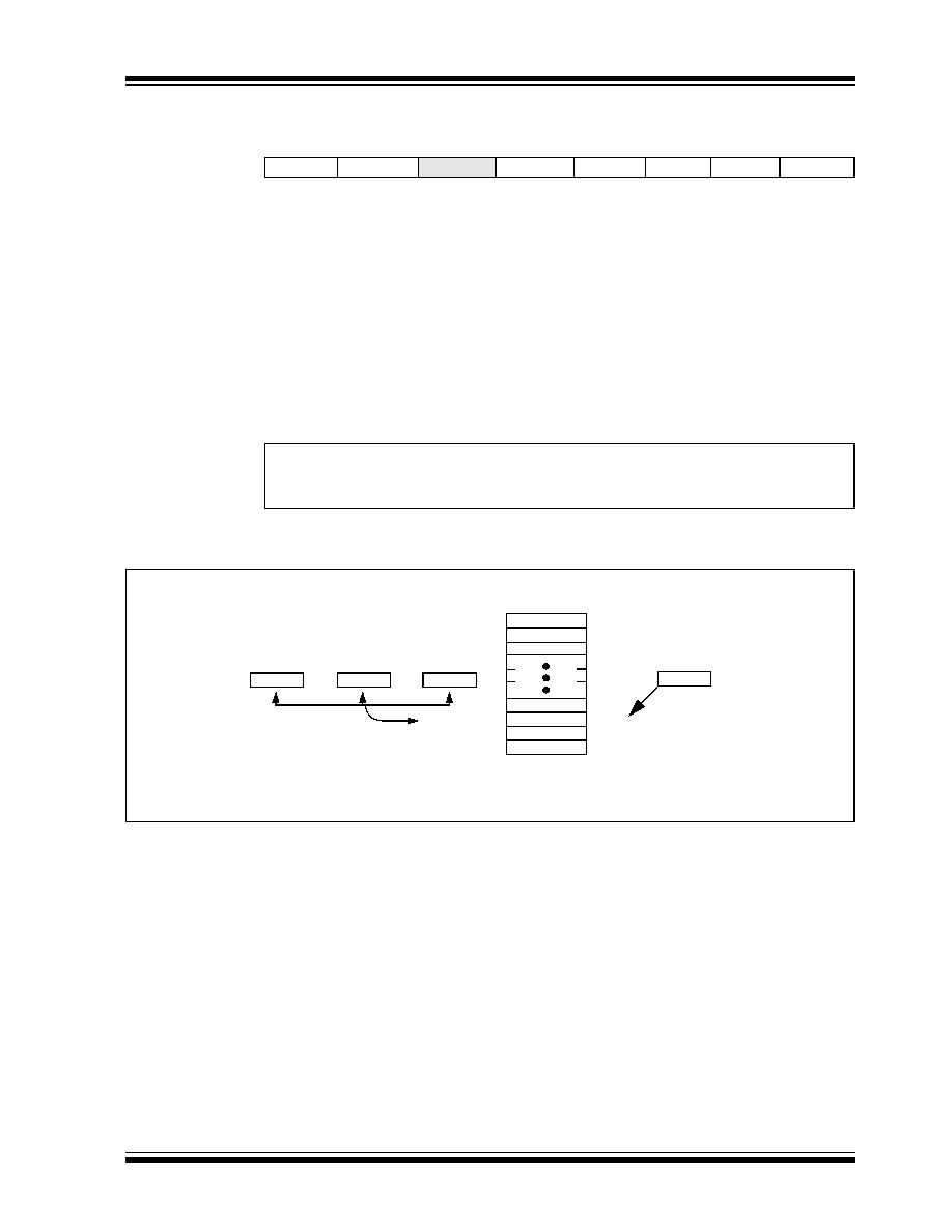
2002 Microchip Technology Inc.
Preliminary
DS41159B-page 39
PIC18FXX8
REGISTER 4-1:
STKPTR - STACK POINTER REGISTER
FIGURE 4-3:
RETURN ADDRESS STACK AND ASSOCIATED REGISTERS
R/C-0
R/C-0
U-0
R/W-0
R/W-0
R/W-0
R/W-0
R/W-0
STKFUL
STKUNF
--
SP4
SP3
SP2
SP1
SP0
bit 7
bit 0
bit 7
STKFUL: Stack Full Flag bit
1
= Stack became full or overflowed
0
= Stack has not become full or overflowed
bit 6
STKUNF: Stack Underflow Flag bit
1
= Stack underflow occurred
0
= Stack underflow did not occur
bit 5
Unimplemented: Read as '0'
bit 4-0
SP4:SP0: Stack Pointer Location bits
Note:
Bit 7 and bit 6 need to be cleared following a stack underflow or a stack overflow.
Legend:
R
= Readable bit
W = Writable bit
U = Unimplemented bit, read as `0'
- n = Value at POR
'1' = Bit is set
'0' = Bit is cleared
C = Clearable bit
00011
001A34h
11111
11110
11101
00010
00001
00000
(1)
00010
Return Address Stack
Top-of-Stack
000D58h
TOSL
TOSH
TOSU
34h
1Ah
00h
STKPTR<4:0>
000000h
Note 1: No RAM associated with this address; always maintained `0's.

PIC18FXX8
DS41159B-page 40
Preliminary
2002 Microchip Technology Inc.
4.2.3
PUSH
AND
POP
INSTRUCTIONS
Since the Top-of-Stack (TOS) is readable and writable,
the ability to push values onto the stack and pull values
off the stack without disturbing normal program execu-
tion is a desirable option. To push the current PC value
onto the stack, a
PUSH
instruction can be executed.
This will increment the stack pointer and load the cur-
rent PC value onto the stack. TOSU, TOSH and TOSL
can then be modified to place a return address on the
stack.
The
POP
instruction discards the current TOS by decre-
menting the stack pointer. The previous value pushed
onto the stack then becomes the TOS value.
4.2.4
STACK FULL/UNDERFLOW RESETS
These RESETS are enabled by programming the
STVREN configuration bit. When the STVREN bit is
disabled, a full or underflow condition will set the appro-
priate STKFUL or STKUNF bit, but not cause a device
RESET. When the STVREN bit is enabled, a full or
underflow condition will set the appropriate STKFUL or
STKUNF bit and then cause a device RESET. The
STKFUL or STKUNF bits are only cleared by the user
software or a POR.
4.3
Fast Register Stack
A "fast return" option is available for interrupts and
calls. A fast register stack is provided for the STATUS,
WREG and BSR registers and is only one layer in
depth. The stack is not readable or writable and is
loaded with the current value of the corresponding reg-
ister when the processor vectors for an interrupt. The
values in the fast register stack are then loaded back
into the working registers if the
fast return
instruction is used to return from the interrupt.
A low or high priority interrupt source will push values
into the stack registers. If both low and high priority
interrupts are enabled, the stack registers cannot be
used reliably for low priority interrupts. If a high priority
interrupt occurs while servicing a low priority interrupt,
the stack register values stored by the low priority
interrupt will be overwritten.
If high priority interrupts are not disabled during low pri-
ority interrupts, users must save the key registers in
software during a low priority interrupt.
If no interrupts are used, the fast register stack can be
used to restore the STATUS, WREG and BSR registers
at the end of a subroutine call. To use the fast register
stack for a subroutine call, a
fast call
instruction
must be executed.
Example 4-1 shows a source code example that uses
the fast register stack.
EXAMPLE 4-1:
FAST REGISTER STACK
CODE EXAMPLE
4.4
PCL, PCLATH and PCLATU
The program counter (PC) specifies the address of the
instruction to fetch for execution. The PC is 21-bits
wide. The low byte is called the PCL register. This reg-
ister is readable and writable. The high byte is called
the PCH register. This register contains the PC<15:8>
bits and is not directly readable or writable. Updates to
the PCH register may be performed through the
PCLATH register. The upper byte is called PCU. This
register contains the PC<20:16> bits and is not directly
readable or writable. Updates to the PCU register may
be performed through the PCLATU register.
The PC addresses bytes in the program memory. To
prevent the PC from becoming misaligned with word
instructions, the LSb of PCL is fixed to a value of '0'.
The PC increments by 2 to address sequential instruc-
tions in the program memory.
The
CALL, RCALL, GOTO
and program branch
instructions write to the program counter directly. For
these instructions, the contents of PCLATH and
PCLATU are not transferred to the program counter.
The contents of PCLATH and PCLATU will be trans-
ferred to the program counter by an operation that
writes PCL. Similarly, the upper two bytes of the pro-
gram counter will be transferred to PCLATH and
PCLATU by an operation that reads PCL. This is useful
for computed offsets to the PC (see Section 4.8.1).
CALL SUB1, FAST
;STATUS, WREG, BSR
;SAVED IN FAST REGISTER
;STACK
�
�
SUB1
�
�
�
RETURN FAST
;RESTORE VALUES SAVED
;IN FAST REGISTER STACK
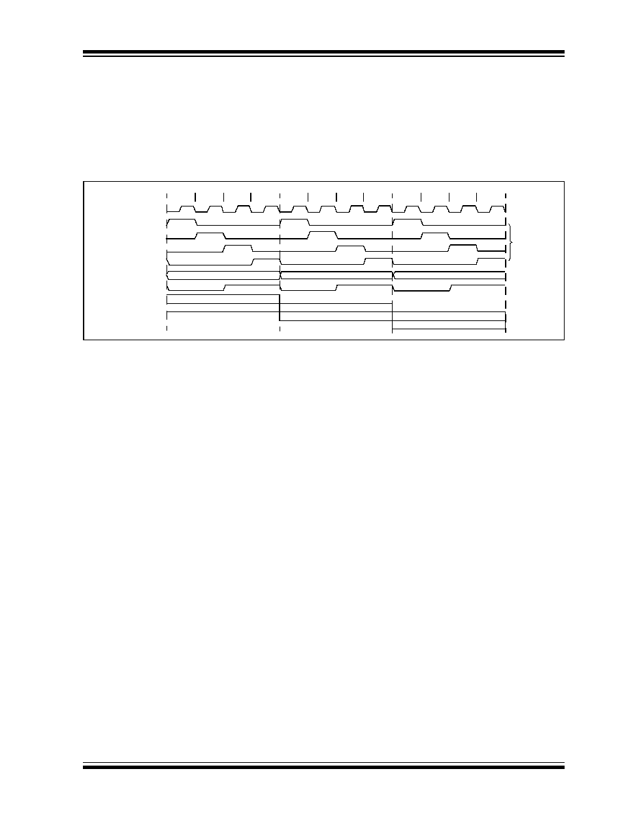
2002 Microchip Technology Inc.
Preliminary
DS41159B-page 41
PIC18FXX8
4.5
Clocking Scheme/Instruction
Cycle
The clock input (from OSC1) is internally divided by
four to generate four non-overlapping quadrature
clocks, namely Q1, Q2, Q3 and Q4. Internally, the pro-
gram counter (PC) is incremented every Q1, the
instruction is fetched from the program memory and
latched into the instruction register in Q4. The instruc-
tion is decoded and executed during the following Q1
through Q4. The clocks and instruction execution flow
are shown in Figure 4-4.
FIGURE 4-4:
CLOCK/INSTRUCTION CYCLE
4.6
Instruction Flow/Pipelining
An "Instruction Cycle" consists of four Q cycles (Q1,
Q2, Q3 and Q4). The instruction fetch and execute are
pipelined such that fetch takes one instruction cycle,
while decode and execute take another instruction
cycle. However, due to the pipelining, each instruction
effectively executes in one cycle. If an instruction
causes the program counter to change (e.g.,
GOTO
),
two cycles are required to complete the instruction
(Example 4-2).
A fetch cycle begins with the program counter (PC)
incrementing in Q1.
In the execution cycle, the fetched instruction is latched
into the "Instruction Register" (IR) in cycle Q1. This
instruction is then decoded and executed during the
Q2, Q3, and Q4 cycles. Data memory is read during Q2
(operand read) and written during Q4 (destination
write).
4.7
Instructions in Program Memory
The program memory is addressed in bytes. Instruc-
tions are stored as two bytes or four bytes in program
memory. The Least Significant Byte of an instruction
word is always stored in a program memory location
with an even address (LSB = '
0
'). Figure 4-3 shows an
example of how instruction words are stored in the pro-
gram memory. To maintain alignment with instruction
boundaries, the PC increments in steps of 2 and the
LSB will always read '
0
' (see Section 4.4).
The
CALL
and
GOTO
instructions have an absolute pro-
gram memory address embedded into the instruction.
Since instructions are always stored on word bound-
aries, the data contained in the instruction is a word
address. The word address is written to PC<20:1>,
which accesses the desired byte address in program
memory. Instruction #2 in Example 4-3 shows how the
instruction "
GOTO 000006h
" is encoded in the program
memory. Program branch instructions that encode a
relative address offset operate in the same manner.
The offset value stored in a branch instruction repre-
sents the number of single word instructions by which
the PC will be offset. Section 25.0 provides further
details of the instruction set.
Q1
Q2
Q3
Q4
Q1
Q2
Q3
Q4
Q1
Q2
Q3
Q4
OSC1
Q1
Q2
Q3
Q4
PC
OSC2/CLKO
(RC Mode)
PC
PC+2
PC+4
Fetch INST (PC)
Execute INST (PC-2)
Fetch INST (PC+2)
Execute INST (PC)
Fetch INST (PC+4)
Execute INST (PC+2)
Internal
Phase
Clock
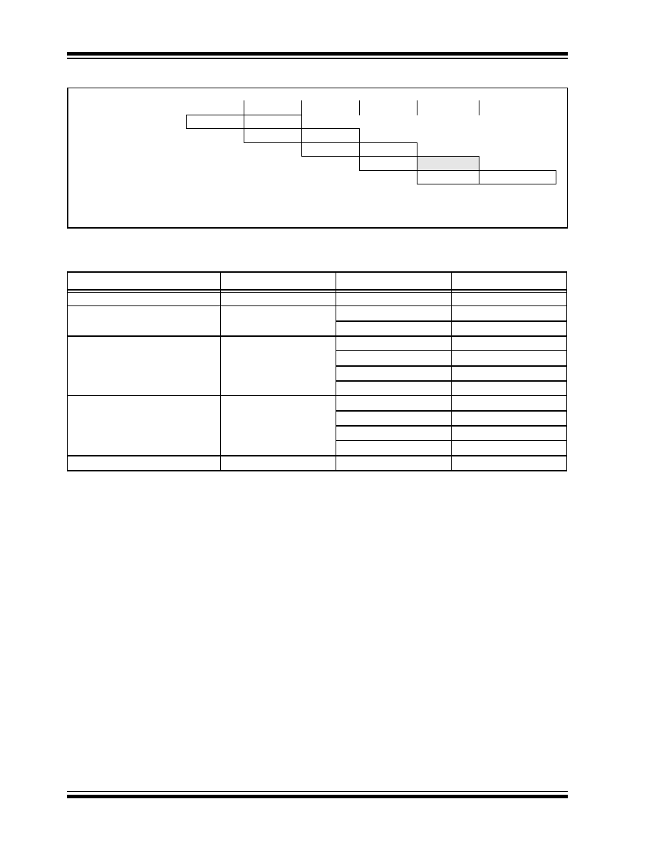
PIC18FXX8
DS41159B-page 42
Preliminary
2002 Microchip Technology Inc.
EXAMPLE 4-2:
INSTRUCTION PIPELINE FLOW
EXAMPLE 4-3:
INSTRUCTIONS IN PROGRAM MEMORY
Note:
All instructions are single cycle, except for any program branches. These take two cycles, since the fetch instruction
is "flushed" from the pipeline while the new instruction is being fetched and then executed.
T
CY
0
T
CY
1
T
CY
2
T
CY
3
T
CY
4
T
CY
5
1. MOVLW 55h
Fetch 1
Execute 1
2. MOVWF PORTB
Fetch 2
Execute 2
3. BRA SUB_1
Fetch 3
Execute 3
4. BSF PORTA, BIT3 (Forced NOP)
Fetch 4
Flush
5. Instruction @ address SUB_1
Fetch SUB_1
Execute SUB_1
Instruction
Opcode
Memory
Address
--
000007h
MOVLW 055h
0E55h
55h
000008h
0Eh
000009h
GOTO 000006h
EF03h, F000h
03h
00000Ah
EFh
00000Bh
00h
00000Ch
F0h
00000Dh
MOVFF 123h, 456h
C123h, F456h
23h
00000Eh
C1h
00000Fh
56h
000010h
F4h
000011h
--
000012h
2002 Microchip Technology Inc.
Preliminary
DS41159B-page 43
PIC18FXX8
4.7.1
TWO-WORD INSTRUCTIONS
The PIC18FXX8 devices have 4 two-word instructions:
MOVFF, CALL, GOTO
and
LFSR
. The 4 Most Signifi-
cant bits of the second word are set to `
1
's, and indicate
a special
NOP
instruction. The lower 12 bits of the sec-
ond word contain the data to be used by the instruction.
If the first word of the instruction is executed, the data
in the second word is accessed. If the second word of
the instruction is executed by itself (first word was
skipped), it will execute as a
NOP
. This action is neces-
sary when the two-word instruction is preceded by a
conditional instruction that changes the PC. A program
example that demonstrates this concept is shown in
Example 4-4. Refer to Section 25.0 for further details of
the instruction set.
4.8
Lookup Tables
Lookup tables are implemented two ways. These are:
� Computed
GOTO
� Table Reads
4.8.1
COMPUTED
GOTO
A computed
GOTO
is accomplished by adding an offset
to the program counter (
ADDWF PCL
).
The
ADDWF PCL
instruction does not update PCLATH/
PCLATU. A read operation on PCL must be performed
prior to the
ADDWF PCL
.
A lookup table can be formed with an
ADDWF PCL
instruction and a group of
RETLW 0xnn
instructions.
WREG is loaded with an offset into the table before
executing a call to that table. The first instruction of the
called routine is the
ADDWF PCL
instruction. The next
instruction executed will be one of the
RETLW 0xnn
instructions that returns the value
0xnn
to the calling
function.
The offset value (value in WREG) specifies the number
of bytes that the program counter should advance.
In this method, only one data byte may be stored in
each instruction location and room on the return
address stack is required.
4.8.2
TABLE READS/TABLE WRITES
A better method of storing data in program memory
allows 2 bytes of data to be stored in each instruction
location.
Lookup table data may be stored as 2 bytes per pro-
gram word by using table reads and writes. The table
pointer (TBLPTR) specifies the byte address and the
table latch (TABLAT) contains the data that is read
from, or written to, program memory. Data is
transferred to/from program memory, one byte at a
time.
A description of the Table Read/Table Write operation
is shown in Section 6.1.
EXAMPLE 4-4:
TWO-WORD INSTRUCTIONS
Warning: The LSb of PCL is fixed to a value of `0'.
Hence, computed
GOTO
to an odd
address is not possible.
CASE 1:
Object Code
Source Code
0110 0110 0000 0000
TSTFSZ
REG1
; is RAM location 0?
1100 0001 0010 0011
MOVFF
REG1, REG2 ; No, execute 2-word instruction
1111 0100 0101 0110
; 2nd operand holds address of REG2
0010 0100 0000 0000
ADDWF
REG3
; continue code
CASE 2:
Object Code
Source Code
0110 0110 0000 0000
TSTFSZ
REG1
; is RAM location 0?
1100 0001 0010 0011
MOVFF
REG1, REG2 ; Yes
1111 0100 0101 0110
; 2nd operand becomes NOP
0010 0100 0000 0000
ADDWF
REG3
; continue code

PIC18FXX8
DS41159B-page 44
Preliminary
2002 Microchip Technology Inc.
4.9
Data Memory Organization
The data memory is implemented as static RAM. Each
register in the data memory has a 12-bit address,
allowing up to 4096 bytes of data memory. Figure 4-6
shows the data memory organization for the
PIC18FXX8 devices.
The data memory map is divided into as many as 16
banks that contain 256 bytes each. The lower 4 bits of
the Bank Select Register (BSR<3:0>) select which
bank will be accessed. The upper 4 bits for the BSR are
not implemented.
The data memory contains Special Function Registers
(SFRs) and General Purpose Registers (GPRs). The
SFRs are used for control and status of the controller
and peripheral functions, while GPR's are used for data
storage and scratch pad operations in the user's appli-
cation. The SFR's start at the last location of Bank 15
(FFFh) and grow downwards. GPRs start at the first
location of Bank 0 and grow upwards. Any read of an
unimplemented location will read as '
0
's.
The entire data memory may be accessed directly, or
indirectly. Direct addressing may require the use of the
BSR register. Indirect addressing requires the use of
the File Select Register (FSR). Each FSR holds a
12-bit address value that can be used to access any
location in the Data Memory map without banking.
The instruction set and architecture allow operations
across all banks. This may be accomplished by indirect
addressing or by the use of the
MOVFF
instruction. The
MOVFF
instruction is a two-word/two-cycle instruction,
that moves a value from one register to another.
To ensure that commonly used registers (SFRs and
select GPRs) can be accessed in a single cycle,
regardless of the current BSR values, an Access Bank
is implemented. A segment of Bank 0 and a segment of
Bank 15 comprise the Access RAM. Section 4.10
provides a detailed description of the Access RAM.
4.9.1
GENERAL PURPOSE REGISTER
FILE
The register file can be accessed either directly, or indi-
rectly. Indirect addressing operates through the File
Select Registers (FSR). The operation of indirect
addressing is shown in Section 4.12.
Enhanced MCU devices may have banked memory in
the GPR area. GPRs are not initialized by a Power-on
Reset and are unchanged on all other RESETS.
Data RAM is available for use as GPR registers by all
instructions. Bank 15 (F00h to FFFh) contains SFRs.
All other banks of data memory contain GPR registers,
starting with bank 0.
4.9.2
SPECIAL FUNCTION REGISTERS
The Special Function Registers (SFRs) are registers
used by the CPU and Peripheral Modules for control-
ling the desired operation of the device. These regis-
ters are implemented as static RAM. A list of these
registers is given in Table 4-1.
The SFRs can be classified into two sets: those asso-
ciated with the "core" function and those related to the
peripheral functions. Those registers related to the
"core" are described in this section, while those related
to the operation of the peripheral features are
described in the section of that peripheral feature.
The SFRs are typically distributed among the
peripherals whose functions they control.
The unused SFR locations will be unimplemented and
read as '
0
's. See Table 4-1 for addresses for the SFRs.
2002 Microchip Technology Inc.
Preliminary
DS41159B-page 45
PIC18FXX8
FIGURE 4-5:
DATA MEMORY MAP FOR PIC18F248/448
Bank 0
Bank 1
Bank 14
Bank 15
Data Memory Map
BSR<3:0>
= 0000
= 0001
=
1111
060h
05Fh
F60h
FFFh
00h
5Fh
60h
FFh
Access Bank
F5Fh
F00h
EFFh
1FFh
100h
0FFh
000h
Access RAM
FFh
00h
FFh
00h
FFh
00h
GPR
GPR
SFR
Unused
SFR
Access RAM
Bank 2
to
200h
Unused
Read '00h'
= 1110
= 0010
When a = 0,
the BSR is ignored and
the Access Bank is used.
The first 96 bytes are
General Purpose RAM
(from Bank 0).
The next 160 bytes are
Special Function
Registers (from Bank 15).
When a = 1,
the BSR is used to specify
the RAM location that the
instruction uses.
GPR
FFh
00h
300h
PIC18FXX8
DS41159B-page 46
Preliminary
2002 Microchip Technology Inc.
FIGURE 4-6:
DATA MEMORY MAP FOR PIC18F258/458
Bank 0
Bank 1
Bank 14
Bank 15
Data Memory Map
BSR<3:0>
= 0000
= 0001
= 1110
= 1111
060h
05Fh
F60h
FFFh
00h
5Fh
60h
FFh
Access Bank
Bank 4
Bank 3
Bank 2
F5Fh
F00h
EFFh
3FFh
300h
2FFh
200h
1FFh
100h
0FFh
000h
= 0110
= 0101
= 0011
= 0010
Access RAM
FFh
00h
FFh
00h
FFh
00h
FFh
00h
FFh
00h
FFh
00h
GPR
GPR
GPR
GPR
SFR
SFR
Access Bank high
Access Bank low
Bank 5
GPR
GPR
Bank 6
to
4FFh
400h
5FFh
500h
600h
Unused
Read `00h'
= 0100
(SFR)
When a = 0,
the BSR is ignored and the
Access Bank is used.
The first 96 bytes are
General Purpose RAM
(from Bank 0).
The next 160 bytes are
Special Function Registers
(from Bank 15).
When a = 1,
the BSR is used to specify
the RAM location that the
instruction uses.
(GPR)

2002 Microchip Technology Inc.
Preliminary
DS41159B-page 47
PIC18FXX8
TABLE 4-1:
SPECIAL FUNCTION REGISTER MAP
Address
Name
Address
Name
Address
Name
Address
Name
FFFh TOSU
FDFh INDF2
(2)
FBFh CCPR1H
F9Fh IPR1
FFEh TOSH
FDEh POSTINC2
(2)
FBEh CCPR1L
F9Eh PIR1
FFDh TOSL
FDDh POSTDEC2
(2)
FBDh CCP1CON
F9Dh PIE1
FFCh STKPTR
FDCh PREINC2
(2)
FBCh ECCPR1H
(5)
F9Ch
--
FFBh PCLATU
FDBh PLUSW2
(2)
FBBh ECCPR1L
(5)
F9Bh
--
FFAh PCLATH
FDAh FSR2H
FBAh ECCP1CON
(5)
F9Ah
--
FF9h PCL
FD9h FSR2L
FB9h
--
F99h
--
FF8h TBLPTRU
FD8h STATUS
FB8h
--
F98h
--
FF7h TBLPTRH
FD7h TMR0H
FB7h ECCP1DEL
(5)
F97h
--
FF6h TBLPTRL
FD6h TMR0L
FB6h ECCPAS
(5)
F96h TRISE
(5)
FF5h TABLAT
FD5h T0CON
FB5h CVRCON
(5)
F95h TRISD
(5)
FF4h PRODH
FD4h
--
FB4h CMCON
(5)
F94h TRISC
FF3h PRODL
FD3h OSCCON
FB3h TMR3H
F93h TRISB
FF2h INTCON
FD2h LVDCON
FB2h TMR3L
F92h TRISA
FF1h INTCON2
FD1h WDTCON
FB1h T3CON
F91h
--
FF0h INTCON3
FD0h RCON
FB0h
--
F90h
--
FEFh INDF0
(2)
FCFh TMR1H
FAFh SPBRG
F8Fh
--
FEEh POSTINC0
(2)
FCEh TMR1L
FAEh RCREG
F8Eh
--
FEDh POSTDEC0
(2)
FCDh T1CON
FADh TXREG
F8Dh LATE
(5)
FECh PREINC0
(2)
FCCh TMR2
FACh TXSTA
F8Ch LATD
(5)
FEBh PLUSW0
(2)
FCBh PR2
FABh RCSTA
F8Bh LATC
FEAh FSR0H
FCAh T2CON
FAAh
--
F8Ah LATB
FE9h FSR0L
FC9h SSPBUF
FA9h
EEADR
F89h LATA
FE8h WREG
FC8h SSPADD
FA8h
EEDATA
F88h
--
FE7h INDF1
(2)
FC7h SSPSTAT
FA7h
EECON2
F87h
--
FE6h POSTINC1
(2)
FC6h SSPCON1
FA6h
EECON1
F86h
--
FE5h POSTDEC1
(2)
FC5h SSPCON2
FA5h
IPR3
F85h
--
FE4h PREINC1
(2)
FC4h ADRESH
FA4h
PIR3
F84h PORTE
(5)
FE3h PLUSW1
(2)
FC3h ADRESL
FA3h
PIE3
F83h PORTD
(5)
FE2h FSR1H
FC2h ADCON0
FA2h
IPR2
F82h PORTC
FE1h FSR1L
FC1h ADCON1
FA1h
PIR2
F81h PORTB
FE0h BSR
FC0h
--
FA0h
PIE2
F80h PORTA
Note 1: Unimplemented registers are read as '0'.
2: This is not a physical register.
3: Contents of register are dependent on WIN2:WIN0 bits in CANCON register.
4: CANSTAT register is repeated in these locations to simplify application firmware. Unique names are given
for each instance of the CANSTAT register, due to the Microchip Header file requirement.
5: These registers are not implemented on the PIC18F248 and PIC18F258.
PIC18FXX8
DS41159B-page 48
Preliminary
2002 Microchip Technology Inc.
F7Fh
--
F5Fh
--
F3Fh
--
F1Fh RXM1EIDL
F7Eh
--
F5Eh CANSTATRO1
(4)
F3Eh CANSTATRO3
(4)
F1Eh RXM1EIDH
F7Dh
--
F5Dh RXB1D7
F3Dh TXB1D7
F1Dh RXM1SIDL
F7Ch
--
F5Ch RXB1D6
F3Ch TXB1D6
F1Ch RXM1SIDH
F7Bh
--
F5Bh RXB1D5
F3Bh TXB1D5
F1Bh RXM0EIDL
F7Ah
--
F5Ah RXB1D4
F3Ah TXB1D4
F1Ah RXM0EIDH
F79h
--
F59h
RXB1D3
F39h
TXB1D3
F19h RXM0SIDL
F78h
--
F58h
RXB1D2
F38h
TXB1D2
F18h RXM0SIDH
F77h
--
F57h
RXB1D1
F37h
TXB1D1
F17h RXF5EIDL
F76h TXERRCNT
F56h
RXB1D0
F36h
TXB1D0
F16h RXF5EIDH
F75h RXERRCNT
F55h
RXB1DLC
F35h
TXB1DLC
F15h RXF5SIDL
F74h COMSTAT
F54h
RXB1EIDL
F34h
TXB1EIDL
F14h RXF5SIDH
F73h CIOCON
F53h
RXB1EIDH
F33h
TXB1EIDH
F13h RXF4EIDL
F72h BRGCON3
F52h
RXB1SIDL
F32h
TXB1SIDL
F12h RXF4EIDH
F71h BRGCON2
F51h
RXB1SIDH
F31h
TXB1SIDH
F11h RXF4SIDL
F70h BRGCON1
F50h
RXB1CON
F30h
TXB1CON
F10h RXF4SIDH
F6Fh CANCON
F4Fh
--
F2Fh
--
F0Fh RXF3EIDL
F6Eh CANSTAT
F4Eh CANSTATRO2
(4)
F2Eh CANSTATRO4
(4)
F0Eh RXF3EIDH
F6Dh RXB0D7
(3)
F4Dh TXB0D7
F2Dh TXB2D7
F0Dh RXF3SIDL
F6Ch RXB0D6
(3)
F4Ch TXB0D6
F2Ch TXB2D6
F0Ch RXF3SIDH
F6Bh RXB0D5
(3)
F4Bh TXB0D5
F2Bh TXB2D5
F0Bh RXF2EIDL
F6Ah RXB0D4
(3)
F4Ah TXB0D4
F2Ah TXB2D4
F0Ah RXF2EIDH
F69h RXB0D3
(3)
F49h
TXB0D3
F29h
TXB2D3
F09h RXF2SIDL
F68h RXB0D2
(3)
F48h
TXB0D2
F28h
TXB2D2
F08h RXF2SIDH
F67h RXB0D1
(3)
F47h
TXB0D1
F27h
TXB2D1
F07h RXF1EIDL
F66h RXB0D0
(3)
F46h
TXB0D0
F26h
TXB2D0
F06h RXF1EIDH
F65h RXB0DLC
(3)
F45h
TXB0DLC
F25h
TXB2DLC
F05h RXF1SIDL
F64h RXB0EIDL
(3)
F44h
TXB0EIDL
F24h
TXB2EIDL
F04h RXF1SIDH
F63h RXB0EIDH
(3)
F43h
TXB0EIDH
F23h
TXB2EIDH
F03h RXF0EIDL
F62h RXB0SIDL
(3)
F42h
TXB0SIDL
F22h
TXB2SIDL
F02h RXF0EIDH
F61h RXB0SIDH
(3)
F41h
TXB0SIDH
F21h
TXB2SIDH
F01h RXF0SIDL
F60h RXB0CON
(3)
F40h
TXB0CON
F20h
TXB2CON
F00h RXF0SIDH
Note:
Shaded registers are available in Bank 15, while the rest are in Access Bank low.
TABLE 4-1:
SPECIAL FUNCTION REGISTER MAP (CONTINUED)
Address
Name Address
Name
Address
Name
Address
Name
Note 1: Unimplemented registers are read as '0'.
2: This is not a physical register.
3: Contents of register are dependent on WIN2:WIN0 bits in CANCON register.
4: CANSTAT register is repeated in these locations to simplify application firmware. Unique names are given
for each instance of the CANSTAT register, due to the Microchip Header file requirement.
5: These registers are not implemented on the PIC18F248 and PIC18F258.
2002 Microchip Technology Inc.
Preliminary
DS41159B-page 49
PIC18FXX8
TABLE 4-2:
REGISTER FILE SUMMARY
File Name
Bit 7
Bit 6
Bit 5
Bit 4
Bit 3
Bit 2
Bit 1
Bit 0
Value on
POR, BOR
Details on
Page:
TOSU
--
--
--
Top-of-Stack Upper Byte (TOS<20:16>)
---0 0000
30, 38
TOSH
Top-of-Stack High Byte (TOS<15:8>)
0000 0000
30, 38
TOSL
Top-of-Stack Low Byte (TOS<7:0>)
0000 0000
30, 38
STKPTR
STKFUL
STKUNF
--
Return Stack Pointer
00-0 0000
30, 39
PCLATU
--
--
bit21
(2)
Holding Register for PC<20:16>
---0 0000
30, 40
PCLATH
Holding Register for PC<15:8>
0000 0000
30, 40
PCL
PC Low Byte (PC<7:0>)
0000 0000
30, 40
TBLPTRU
--
--
bit21
(2)
Program Memory Table Pointer Upper Byte (TBLPTR<20:16>)
--00 0000
30, 68
TBLPTRH
Program Memory Table Pointer High Byte (TBLPTR<15:8>)
0000 0000
30, 68
TBLPTRL
Program Memory Table Pointer Low Byte (TBLPTR<7:0>)
0000 0000
30, 68
TABLAT
Program Memory Table Latch
0000 0000
30, 68
PRODH
Product Register High Byte
xxxx xxxx
30, 75
PRODL
Product Register Low Byte
xxxx xxxx
30, 75
INTCON
GIE/GIEH
PEIE/GIEL
TMR0IE
INT0IE
RBIE
TMR0IF
INT0IF
RBIF
0000 000x
30, 79
INTCON2
RBPU
INTEDG0
INTEDG1
--
--
TMR0IP
--
RBIP
111- -1-1
30, 80
INTCON3
INT2IP
INT1IP
--
INT2IE
INT1IE
--
INT2IF
INT1IF
11-1 0-00
30, 81
INDF0
Uses contents of FSR0 to address data memory - value of FSR0 not changed (not a physical register)
n/a
30, 55
POSTINC0
Uses contents of FSR0 to address data memory - value of FSR0 post-incremented (not a physical register)
n/a
30, 55
POSTDEC0
Uses contents of FSR0 to address data memory - value of FSR0 post-incremented (not a physical register)
n/a
30, 55
PREINC0
Uses contents of FSR0 to address data memory - value of FSR0 pre-incremented (not a physical register)
n/a
30, 55
PLUSW0
Uses contents of FSR0 to address data memory - value of FSR0 offset by W (not a physical register)
n/a
30, 55
FSR0H
--
--
--
--
Indirect Data Memory Address Pointer 0 High
---- xxxx
30, 55
FSR0L
Indirect Data Memory Address Pointer 0 Low Byte
xxxx xxxx
30, 55
WREG
Working Register
uuuu uuuu
30, 55
INDF1
Uses contents of FSR1 to address data memory - value of FSR1 not changed (not a physical register)
n/a
30, 55
POSTINC1
Uses contents of FSR1 to address data memory - value of FSR1 post-incremented (not a physical register)
n/a
30, 55
POSTDEC1
Uses contents of FSR1 to address data memory - value of FSR1 post-incremented (not a physical register)
n/a
30, 55
PREINC1
Uses contents of FSR1 to address data memory - value of FSR1 pre-incremented (not a physical register)
n/a
30, 55
PLUSW1
Uses contents of FSR1 to address data memory - value of FSR1 offset by W (not a physical register) -
n/a
30, 55
FSR1H
--
--
--
--
Indirect Data Memory Address Pointer 1 High
---- xxxx
31, 55
FSR1L
Indirect Data Memory Address Pointer 1 Low Byte
xxxx xxxx
31, 55
BSR
--
--
--
--
Bank Select Register
---- 0000
31, 54
INDF2
Uses contents of FSR2 to address data memory - value of FSR2 not changed (not a physical register)
n/a
31, 55
POSTINC2
Uses contents of FSR2 to address data memory - value of FSR2 post-incremented (not a physical register)
n/a
31, 55
POSTDEC2
Uses contents of FSR2 to address data memory - value of FSR2 post-incremented (not a physical register)
n/a
31, 55
PREINC2
Uses contents of FSR2 to address data memory - value of FSR2 pre-incremented (not a physical register)
n/a
31, 55
PLUSW2
Uses contents of FSR2 to address data memory - value of FSR2 offset by W (not a physical register) -
n/a
31, 55
FSR2H
--
--
--
--
Indirect Data Memory Address Pointer 2 High
---- xxxx
31, 55
FSR2L
Indirect Data Memory Address Pointer 2 Low Byte
xxxx xxxx
31, 55
STATUS
--
--
--
N
OV
Z
DC
C
---x xxxx
31, 57
TMR0H
Timer0 Register High Byte
0000 0000
31, 109
TMR0L
Timer0 Register Low Byte
xxxx xxxx
31, 109
T0CON
TMR0ON
T08BIT
T0CS
T0SE
PSA
T0PS2
T0PS1
T0PS0
1111 1111
31, 107
OSCCON
--
--
--
--
--
--
--
SCS
---- ---0
31, 20
LVDCON
--
--
IRVST
LVDEN
LVDL3
LVDL2
LVDL1
LVDL0
--00 0101
31, 257
WDTCON
--
--
--
--
--
--
--
SWDTEN
---- ---0
31, 268
RCON
IPEN
--
--
RI
TO
PD
POR
BOR
0--1 11qq
31, 58, 91
Legend:
x
= unknown,
u
= unchanged, - = unimplemented,
q
= value depends on condition
Note
1:
These registers or register bits are not implemented on the PIC18F248 and PIC18F258 and read as '0's.
2:
Bit21 of the TBLPTRU allows access to the device configuration bits.
3:
RA6 and associated bits are configured as port pins in RCIO and ECIO Oscillator mode only and read `0' in all other Oscillator
modes.
PIC18FXX8
DS41159B-page 50
Preliminary
2002 Microchip Technology Inc.
TMR1H
Timer1 Register High Byte
xxxx xxxx
31, 113
TMR1L
Timer1 Register Low Byte
xxxx xxxx
31, 113
T1CON
RD16
--
T1CKPS1
T1CKPS0
T1OSCEN
T1SYNC
TMR1CS
TMR1ON
0-00 0000
31, 111
TMR2
Timer2 Register
0000 0000
31, 116
PR2
Timer2 Period Register
1111 1111
31, 116
T2CON
--
TOUTPS3
TOUTPS2
TOUTPS1
TOUTPS0
TMR2ON
T2CKPS1
T2CKPS0
-000 0000
31, 115
SSPBUF
SSP Receive Buffer/Transmit Register
xxxx xxxx
31, 144
SSPADD
SSP Address Register in I
2
C Slave mode. SSP Baud Rate Reload Register in I
2
C Master mode.
0000 0000
31, 150
SSPSTAT
SMP
CKE
D/A
P
S
R/W
UA
BF
0000 0000
31, 142, 151
SSPCON1
WCOL
SSPOV
SSPEN
CKP
SSPM3
SSPM2
SSPM1
SSPM0
0000 0000
31, 143, 152
SSPCON2
GCEN
ACKSTAT
ACKDT
ACKEN
RCEN
PEN
RSEN
SEN
0000 0000
31, 153
ADRESH
A/D Result Register High Byte
xxxx xxxx
32, 239
ADRESL
A/D Result Register Low Byte
xxxx xxxx
32, 239
ADCON0
ADCS1
ADCS0
CHS2
CHS1
CHS0
GO/DONE
--
ADON
0000 00-0
32, 237
ADCON1
ADFM
ADCS2
--
--
PCFG3
PCFG2
PCFG1
PCFG0
00-- 0000
32, 238
CCPR1H
Capture/Compare/PWM Register1 High Byte
xxxx xxxx
32, 122
CCPR1L
Capture/Compare/PWM Register1 Low Byte
xxxx xxxx
32, 122
CCP1CON
--
--
DC1B1
DC1B0
CCP1M3
CCP1M2
CCP1M1
CCP1M0
--00 0000
32, 121
ECCPR1H
(1)
Enhanced Capture/Compare/PWM Register1 High Byte
xxxx xxxx
32, 131
ECCPR1L
(1)
Enhanced Capture/Compare/PWM Register1 Low Byte
xxxx xxxx
32, 131
ECCP1CON
(1)
EPWM1M1
EPWM1M0
EDC1B1
EDC1B0
ECCP1M3 ECCP1M2 ECCP1M1 ECCP1M0
0000 0000
32, 129
ECCP1DEL
(1)
EPDC7
EPDC6
EPDC5
EPDC4
EPDC3
EPDC2
EPDC1
EPDC0
0000 0000
32, 138
ECCPAS
(1)
ECCPASE
ECCPAS2
ECCPAS1
ECCPAS0
PSSAC1
PSSAC0
PSSBD1
PSSBD0
0000 0000
32, 140
CVRCON
(1)
CVREN
CVROE
CVRR
CVRSS
CVR3
CVR2
CVR1
CVR0
0000 0000
32, 251
CMCON
(1)
C2OUT
C1OUT
C2INV
C1INV
CIS
CM2
CM1
CM0
0000 0000
32, 245
TMR3H
Timer3 Register High Byte
xxxx xxxx
32, 119
TMR3L
Timer3 Register Low Byte
xxxx xxxx
32, 119
T3CON
RD16
T3ECCP1
T3CKPS1
T3CKPS0
T3CCP1
T3SYNC
TMR3CS
TMR3ON
0000 0000
32, 117
SPBRG
USART1 Baud Rate Generator
0000 0000
32, 183
RCREG
USART1 Receive Register
0000 0000
32, 189
TXREG
USART1 Transmit Register
0000 0000
32, 187
TXSTA
CSRC
TX9
TXEN
SYNC
--
BRGH
TRMT
TX9D
0000 -010
32, 181
RCSTA
SPEN
RX9
SREN
CREN
ADDEN
FERR
OERR
RX9D
0000 000X
32, 182
EEADR
EEPROM Address Register
xxxx xxxx
32, 59
EEDATA
EEPROM Data Register
xxxx xxxx
32, 59
EECON2
EEPROM Control Register2 (not a physical register)
xxxx xxxx
32, 59
EECON1
EEPGD
CFGS
--
FREE
WRERR
WREN
WR
RD
xx-0 x000
32, 60, 67
IPR3
IRXIP
WAKIP
ERRIP
TXB2IP
TXB1IP
TXB0IP
RXB1IP
RXB0IP
1111 1111
32, 90
PIR3
IRXIF
WAKIF
ERRIF
TXB2IF
TXB1IF
TXB0IF
RXB1IF
RXB0IF
0000 0000
32, 84
PIE3
IRXIE
WAKIE
ERRIE
TXB2IE
TXB1IE
TXB0IE
RXB1IE
RXB0IE
0000 0000
32, 87
IPR2
--
CMIP
--
EEIP
BCLIP
LVDIP
TMR3IP
ECCP1IP
(1)
-1-1 1111
33, 89
PIR2
--
CMIF
--
EEIF
BCLIF
LVDIF
TMR3IF
ECCP1IF
(1)
-0-0 0000
33, 83
PIE2
--
CMIE
--
EEIE
BCLIE
LVDIE
TMR3IE
ECCP1IE
(1)
-0-0 0000
33, 86
TABLE 4-2:
REGISTER FILE SUMMARY (CONTINUED)
File Name
Bit 7
Bit 6
Bit 5
Bit 4
Bit 3
Bit 2
Bit 1
Bit 0
Value on
POR, BOR
Details on
Page:
Legend:
x
= unknown,
u
= unchanged, - = unimplemented,
q
= value depends on condition
Note
1:
These registers or register bits are not implemented on the PIC18F248 and PIC18F258 and read as '0's.
2:
Bit21 of the TBLPTRU allows access to the device configuration bits.
3:
RA6 and associated bits are configured as port pins in RCIO and ECIO Oscillator mode only and read `0' in all other Oscillator
modes.
2002 Microchip Technology Inc.
Preliminary
DS41159B-page 51
PIC18FXX8
IPR1
PSPIP
ADIP
RCIP
TXIP
SSPIP
CCP1IP
TMR2IP
TMR1IP
1111 1111
33, 88
PIR1
PSPIF
ADIF
RCIF
TXIF
SSPIF
CCP1IF
TMR2IF
TMR1IF
0000 0000
33, 82
PIE1
PSPIE
ADIE
RCIE
TXIE
SSPIE
CCP1IE
TMR2IE
TMR1IE
0000 0000
33, 85
TRISE
(1)
IBF
OBF
IBOV
PSPMODE
--
Data Direction bits for PORTE
(1)
0000 -111
33, 103
TRISD
(1)
Data Direction Control Register for PORTD
(1)
1111 1111
33, 100
TRISC
Data Direction Control Register for PORTC
1111 1111
33, 98
TRISB
Data Direction Control Register for PORTB
1111 1111
33, 95
TRISA
(3)
--
Data Direction Control Register for PORTA
--11 1111
33, 93
LATE
(1)
--
--
--
--
--
Read PORTE Data Latch, Write
PORTE Data Latch
(1)
---- -xxx
33, 102
LATD
(1)
Read PORTD Data Latch, Write PORTD Data Latch
(1)
xxxx xxxx
33, 100
LATC
Read PORTC Data Latch, Write PORTC Data Latch
xxxx xxxx
33, 98
LATB
Read PORTB Data Latch, Write PORTB Data Latch
xxxx xxxx
33, 95
LATA
(3)
--
Read PORTA Data Latch, Write PORTA Data Latch
-xxx xxxx
33, 93
PORTE
(1)
--
--
--
--
--
Read PORTE pins, Write PORTE
Data Latch
(1)
---- -000
33, 102
PORTD
(1)
Read PORTD pins, Write PORTD Data Latch
(1)
xxxx xxxx
33, 100
PORTC
Read PORTC pins, Write PORTC Data Latch
xxxx xxxx
33, 98
PORTB
Read PORTB pins, Write PORTB Data Latch
xxxx xxxx
33, 95
PORTA
(3)
--
Read PORTA pins, Write PORTA Data Latch
-x0x 0000
33, 93
TXERRCNT
TEC7
TEC6
TEC5
TEC4
TEC3
TEC2
TEC1
TEC0
0000 0000
33, 207
RXERRCNT
REC7
REC6
REC5
REC4
REC3
REC2
REC1
REC0
0000 0000
33, 212
COMSTAT
RXB0OVFL RXB1OVFL
TXBO
TXBP
RXBP
TXWARN
RXWARN
EWARN
0000 0000
33, 203
CIOCON
--
--
ENDRHI
CANCAP
--
--
--
--
--00 ----
33, 217
BRGCON3
--
WAKFIL
--
--
--
SEG2PH2 SEG2PH1 SEG2PH0
-0-- -000
33, 217
BRGCON2
SEG2PHTS
SAM
SEG1PH2
SEG1PH1
SEG1PH0
PRSEG2
PRSEG1
PRSEG0
0000 0000
33, 216
BRGCON1
SJW1
SJW0
BRP5
BRP4
BRP3
BRP2
BRP1
BRP0
0000 0000
33, 215
CANCON
REQOP2
REQOP1
REQOP0
ABAT
WIN2
WIN1
WIN0
--
xxxx xxx-
33, 199
CANSTAT
OPMODE2
OPMODE1
OPMODE0
--
ICODE2
ICODE1
ICODE0
--
xxx- xxx-
33, 200
RXB0D7
RXB0D77
RXB0D76
RXB0D75
RXB0D74
RXB0D73
RXB0D72
RXB0D71
RXB0D70
xxxx xxxx
34, 211
RXB0D6
RXB0D67
RXB0D66
RXB0D65
RXB0D64
RXB0D63
RXB0D62
RXB0D61
RXB0D60
xxxx xxxx
34, 211
RXB0D5
RXB0D57
RXB0D56
RXB0D55
RXB0D54
RXB0D53
RXB0D52
RXB0D51
RXB0D50
xxxx xxxx
34, 211
RXB0D4
RXB0D47
RXB0D46
RXB0D45
RXB0D44
RXB0D43
RXB0D42
RXB0D41
RXB0D40
xxxx xxxx
34, 211
RXB0D3
RXB0D37
RXB0D36
RXB0D35
RXB0D34
RXB0D33
RXB0D32
RXB0D31
RXB0D30
xxxx xxxx
34, 211
RXB0D2
RXB0D27
RXB0D26
RXB0D25
RXB0D24
RXB0D23
RXB0D22
RXB0D21
RXB0D20
xxxx xxxx
34, 211
RXB0D1
RXB0D17
RXB0D16
RXB0D15
RXB0D14
RXB0D13
RXB0D12
RXB0D11
RXB0D10
xxxx xxxx
34, 211
RXB0D0
RXB0D07
RXB0D06
RXB0D05
RXB0D04
RXB0D03
RXB0D02
RXB0D01
RXB0D00
xxxx xxxx
34, 211
RXB0DLC
--
RXRTR
RB1
RB0
DLC3
DLC2
DLC1
DLC0
-xxx xxxx
34, 211
RXB0EIDL
EID7
EID6
EID5
EID4
EID3
EID2
EID1
EID0
xxxx xxxx
34, 210
RXB0EIDH
EID15
EID14
EID13
EID12
EID11
EID10
EID9
EID8
xxxx xxxx
34, 210
RXB0SIDL
SID2
SID1
SID0
SRR
EXID
--
EID17
EID16
xxxx x-xx
34, 210
RXB0SIDH
SID10
SID9
SID8
SID7
SID6
SID5
SID4
SID3
xxxx xxxx
34, 209
RXB0CON
RXFUL
RXM1
RXM0
--
RXRTRRO RXB0DBEN
JTOFF
FILHIT0
000- 0000
34, 208
TABLE 4-2:
REGISTER FILE SUMMARY (CONTINUED)
File Name
Bit 7
Bit 6
Bit 5
Bit 4
Bit 3
Bit 2
Bit 1
Bit 0
Value on
POR, BOR
Details on
Page:
Legend:
x
= unknown,
u
= unchanged, - = unimplemented,
q
= value depends on condition
Note
1:
These registers or register bits are not implemented on the PIC18F248 and PIC18F258 and read as '0's.
2:
Bit21 of the TBLPTRU allows access to the device configuration bits.
3:
RA6 and associated bits are configured as port pins in RCIO and ECIO Oscillator mode only and read `0' in all other Oscillator
modes.

PIC18FXX8
DS41159B-page 52
Preliminary
2002 Microchip Technology Inc.
CANSTATRO1 OPMODE2
OPMODE1
OPMODE0
--
ICODE2
ICODE1
ICODE0
--
xxx- xxx-
33, 200
RXB1D7
RXB1D77
RXB1D76
RXB1D75
RXB1D74
RXB1D73
RXB1D72
RXB1D71
RXB1D70
xxxx xxxx
34, 211
RXB1D6
RXB1D67
RXB1D66
RXB1D65
RXB1D64
RXB1D63
RXB1D62
RXB1D61
RXB1D60
xxxx xxxx
34, 211
RXB1D5
RXB1D57
RXB1D56
RXB1D55
RXB1D54
RXB1D53
RXB1D52
RXB1D51
RXB1D50
xxxx xxxx
34, 211
RXB1D4
RXB1D47
RXB1D46
RXB1D45
RXB1D44
RXB1D43
RXB1D42
RXB1D41
RXB1D40
xxxx xxxx
34, 211
RXB1D3
RXB1D37
RXB1D36
RXB1D35
RXB1D34
RXB1D33
RXB1D32
RXB1D31
RXB1D30
xxxx xxxx
34, 211
RXB1D2
RXB1D27
RXB1D26
RXB1D25
RXB1D24
RXB1D23
RXB1D22
RXB1D21
RXB1D20
xxxx xxxx
34, 211
RXB1D1
RXB1D17
RXB1D16
RXB1D15
RXB1D14
RXB1D13
RXB1D12
RXB1D11
RXB1D10
xxxx xxxx
34, 211
RXB1D0
RXB1D07
RXB1D06
RXB1D05
RXB1D04
RXB1D03
RXB1D02
RXB1D01
RXB1D00
xxxx xxxx
34, 211
RXB1DLC
--
RXRTR
RB1
RB0
DLC3
DLC2
DLC1
DLC0
-xxx xxxx
34, 211
RXB1EIDL
EID7
EID6
EID5
EID4
EID3
EID2
EID1
EID0
xxxx xxxx
34, 210
RXB1EIDH
EID15
EID14
EID13
EID12
EID11
EID10
EID9
EID8
xxxx xxxx
34, 210
RXB1SIDL
SID2
SID1
SID0
SRR
EXID
--
EID17
EID16
xxxx x-xx
34, 210
RXB1SIDH
SID10
SID9
SID8
SID7
SID6
SID5
SID4
SID3
xxxx xxxx
34, 209
RXB1CON
RXFUL
RXM1
RXM0
--
RXRTRRO
FILHIT2
FILHIT1
FILHIT0
000- 0000
34, 209
CANSTATRO2 OPMODE2
OPMODE1
OPMODE0
--
ICODE2
ICODE1
ICODE0
--
xxx- xxx-
33, 200
TXB0D7
TXB0D77
TXB0D76
TXB0D75
TXB0D74
TXB0D73
TXB0D72
TXB0D71
TXB0D70
xxxx xxxx
34, 206
TXB0D6
TXB0D67
TXB0D66
TXB0D65
TXB0D64
TXB0D63
TXB0D62
TXB0D61
TXB0D60
xxxx xxxx
34, 206
TXB0D5
TXB0D57
TXB0D56
TXB0D55
TXB0D54
TXB0D53
TXB0D52
TXB0D51
TXB0D50
xxxx xxxx
34, 206
TXB0D4
TXB0D47
TXB0D46
TXB0D45
TXB0D44
TXB0D43
TXB0D42
TXB0D41
TXB0D40
xxxx xxxx
34, 206
TXB0D3
TXB0D37
TXB0D36
TXB0D35
TXB0D34
TXB0D33
TXB0D32
TXB0D31
TXB0D30
xxxx xxxx
34, 206
TXB0D2
TXB0D27
TXB0D26
TXB0D25
TXB0D24
TXB0D23
TXB0D22
TXB0D21
TXB0D20
xxxx xxxx
34, 206
TXB0D1
TXB0D17
TXB0D16
TXB0D15
TXB0D14
TXB0D13
TXB0D12
TXB0D11
TXB0D10
xxxx xxxx
34, 206
TXB0D0
TXB0D07
TXB0D06
TXB0D05
TXB0D04
TXB0D03
TXB0D02
TXB0D01
TXB0D00
xxxx xxxx
34, 206
TXB0DLC
--
TXRTR
--
--
DLC3
DLC2
DLC1
DLC0
-x-- xxxx
35, 207
TXB0EIDL
EID7
EID6
EID5
EID4
EID3
EID2
EID1
EID0
xxxx xxxx
35, 206
TXB0EIDH
EID15
EID14
EID13
EID12
EID11
EID10
EID9
EID8
xxxx xxxx
35, 205
TXB0SIDL
SID2
SID1
SID0
--
EXIDE
--
EID17
EID16
xxx- x-xx
35, 205
TXB0SIDH
SID10
SID9
SID8
SID7
SID6
SID5
SID4
SID3
xxxx xxxx
35, 205
TXB0CON
--
TXABT
TXLARB
TXERR
TXREQ
--
TXPRI1
TXPRI0
-000 0-00
35, 204
CANSTATRO3 OPMODE2
OPMODE1
OPMODE0
--
ICODE2
ICODE1
ICODE0
--
xxx- xxx-
33, 200
TXB1D7
TXB1D77
TXB1D76
TXB1D75
TXB1D74
TXB1D73
TXB1D72
TXB1D71
TXB1D70
xxxx xxxx
35, 206
TXB1D6
TXB1D67
TXB1D66
TXB1D65
TXB1D64
TXB1D63
TXB1D62
TXB1D61
TXB1D60
xxxx xxxx
35, 206
TXB1D5
TXB1D57
TXB1D56
TXB1D55
TXB1D54
TXB1D53
TXB1D52
TXB1D51
TXB1D50
xxxx xxxx
35, 206
TXB1D4
TXB1D47
TXB1D46
TXB1D45
TXB1D44
TXB1D43
TXB1D42
TXB1D41
TXB1D40
xxxx xxxx
35, 206
TXB1D3
TXB1D37
TXB1D36
TXB1D35
TXB1D34
TXB1D33
TXB1D32
TXB1D31
TXB1D30
xxxx xxxx
35, 206
TXB1D2
TXB1D27
TXB1D26
TXB1D25
TXB1D24
TXB1D23
TXB1D22
TXB1D21
TXB1D20
xxxx xxxx
35, 206
TXB1D1
TXB1D17
TXB1D16
TXB1D15
TXB1D14
TXB1D13
TXB1D12
TXB1D11
TXB1D10
xxxx xxxx
35, 206
TXB1D0
TXB1D07
TXB1D06
TXB1D05
TXB1D04
TXB1D03
TXB1D02
TXB1D01
TXB1D00
xxxx xxxx
35, 206
TXB1DLC
--
TXRTR
--
--
DLC3
DLC2
DLC1
DLC0
-x-- xxxx
35, 207
TXB1EIDL
EID7
EID6
EID5
EID4
EID3
EID2
EID1
EID0
xxxx xxxx
35, 206
TXB1EIDH
EID15
EID14
EID13
EID12
EID11
EID10
EID9
EID8
xxxx xxxx
35, 205
TXB1SIDL
SID2
SID1
SID0
--
EXIDE
--
EID17
EID16
xxx- x-xx
35, 205
TXB1SIDH
SID10
SID9
SID8
SID7
SID6
SID5
SID4
SID3
xxxx xxxx
35, 205
TXB1CON
--
TXABT
TXLARB
TXERR
TXREQ
--
TXPRI1
TXPRI0
0000 0000
35, 204
TABLE 4-2:
REGISTER FILE SUMMARY (CONTINUED)
File Name
Bit 7
Bit 6
Bit 5
Bit 4
Bit 3
Bit 2
Bit 1
Bit 0
Value on
POR, BOR
Details on
Page:
Legend:
x
= unknown,
u
= unchanged, - = unimplemented,
q
= value depends on condition
Note
1:
These registers or register bits are not implemented on the PIC18F248 and PIC18F258 and read as '0's.
2:
Bit21 of the TBLPTRU allows access to the device configuration bits.
3:
RA6 and associated bits are configured as port pins in RCIO and ECIO Oscillator mode only and read `0' in all other Oscillator
modes.

2002 Microchip Technology Inc.
Preliminary
DS41159B-page 53
PIC18FXX8
CANSTATRO4 OPMODE2
OPMODE1
OPMODE0
--
ICODE2
ICODE1
ICODE0
--
xxx- xxx-
33, 200
TXB2D7
TXB2D77
TXB2D76
TXB2D75
TXB2D74
TXB2D73
TXB2D72
TXB2D71
TXB2D70
xxxx xxxx
35, 206
TXB2D6
TXB2D67
TXB2D66
TXB2D65
TXB2D64
TXB2D63
TXB2D62
TXB2D61
TXB2D60
xxxx xxxx
35, 206
TXB2D5
TXB2D57
TXB2D56
TXB2D55
TXB2D54
TXB2D53
TXB2D52
TXB2D51
TXB2D50
xxxx xxxx
35, 206
TXB2D4
TXB2D47
TXB2D46
TXB2D45
TXB2D44
TXB2D43
TXB2D42
TXB2D41
TXB2D40
xxxx xxxx
35, 206
TXB2D3
TXB2D37
TXB2D36
TXB2D35
TXB2D34
TXB2D33
TXB2D32
TXB2D31
TXB2D30
xxxx xxxx
35, 206
TXB2D2
TXB2D27
TXB2D26
TXB2D25
TXB2D24
TXB2D23
TXB2D22
TXB2D21
TXB2D20
xxxx xxxx
35, 206
TXB2D1
TXB2D17
TXB2D16
TXB2D15
TXB2D14
TXB2D13
TXB2D12
TXB2D11
TXB2D10
xxxx xxxx
35, 206
TXB2D0
TXB2D07
TXB2D06
TXB2D05
TXB2D04
TXB2D03
TXB2D02
TXB2D01
TXB2D00
xxxx xxxx
35, 206
TXB2DLC
--
TXRTR
--
--
DLC3
DLC2
DLC1
DLC0
-x-- xxxx
35, 207
TXB2EIDL
EID7
EID6
EID5
EID4
EID3
EID2
EID1
EID0
xxxx xxxx
35, 206
TXB2EIDH
EID15
EID14
EID13
EID12
EID11
EID10
EID9
EID8
xxxx xxxx
35, 205
TXB2SIDL
SID2
SID1
SID0
--
EXIDE
--
EID17
EID16
xxx- x-xx
35, 205
TXB2SIDH
SID10
SID9
SID8
SID7
SID6
SID5
SID4
SID3
xxxx xxxx
35, 205
TXB2CON
--
TXABT
TXLARB
TXERR
TXREQ
--
TXPRI1
TXPRI0
-000 0-00
35, 204
RXM1EIDL
EID7
EID6
EID5
EID4
EID3
EID2
EID1
EID0
xxxx xxxx
36, 214
RXM1EIDH
EID15
EID14
EID13
EID12
EID11
EID10
EID9
EID8
xxxx xxxx
36, 214
RXM1SIDL
SID2
SID1
SID0
--
--
--
EID17
EID16
xxx- --xx
36, 214
RXM1SIDH
SID10
SID9
SID8
SID7
SID6
SID5
SID4
SID3
xxxx xxxx
36, 213
RXM0EIDL
EID7
EID6
EID5
EID4
EID3
EID2
EID1
EID0
xxxx xxxx
36, 214
RXM0EIDH
EID15
EID14
EID13
EID12
EID11
EID10
EID9
EID8
xxxx xxxx
36, 214
RXM0SIDL
SID2
SID1
SID0
--
--
--
EID17
EID16
xxx- --xx
36, 214
RXM0SIDH
SID10
SID9
SID8
SID7
SID6
SID5
SID4
SID3
xxxx xxxx
36, 213
RXF5EIDL
EID7
EID6
EID5
EID4
EID3
EID2
EID1
EID0
xxxx xxxx
36, 213
RXF5EIDH
EID15
EID14
EID13
EID12
EID11
EID10
EID9
EID8
xxxx xxxx
36, 213
RXF5SIDL
SID2
SID1
SID0
--
EXIDEN
--
EID17
EID16
xxx- x-xx
36, 212
RXF5SIDH
SID10
SID9
SID8
SID7
SID6
SID5
SID4
SID3
xxxx xxxx
36, 212
RXF4EIDL
EID7
EID6
EID5
EID4
EID3
EID2
EID1
EID0
xxxx xxxx
36, 213
RXF4EIDH
EID15
EID14
EID13
EID12
EID11
EID10
EID9
EID8
xxxx xxxx
36, 213
RXF4SIDL
SID2
SID1
SID0
--
EXIDEN
--
EID17
EID16
xxx- x-xx
36, 212
RXF4SIDH
SID10
SID9
SID8
SID7
SID6
SID5
SID4
SID3
xxxx xxxx
36, 212
RXF3EIDL
EID7
EID6
EID5
EID4
EID3
EID2
EID1
EID0
xxxx xxxx
36, 213
RXF3EIDH
EID15
EID14
EID13
EID12
EID11
EID10
EID9
EID8
xxxx xxxx
36, 213
RXF3SIDL
SID2
SID1
SID0
--
EXIDEN
--
EID17
EID16
xxx- x-xx
36, 212
RXF3SIDH
SID10
SID9
SID8
SID7
SID6
SID5
SID4
SID3
xxxx xxxx
36, 212
RXF2EIDL
EID7
EID6
EID5
EID4
EID3
EID2
EID1
EID0
xxxx xxxx
36, 213
RXF2EIDH
EID15
EID14
EID13
EID12
EID11
EID10
EID9
EID8
xxxx xxxx
36, 213
RXF2SIDL
SID2
SID1
SID0
--
EXIDEN
--
EID17
EID16
xxx- x-xx
36, 212
RXF2SIDH
SID10
SID9
SID8
SID7
SID6
SID5
SID4
SID3
xxxx xxxx
36, 212
RXF1EIDL
EID7
EID6
EID5
EID4
EID3
EID2
EID1
EID0
xxxx xxxx
36, 213
RXF1EIDH
EID15
EID14
EID13
EID12
EID11
EID10
EID9
EID8
xxxx xxxx
36, 213
RXF1SIDL
SID2
SID1
SID0
--
EXIDEN
--
EID17
EID16
xxx- x-xx
36, 212
RXF1SIDH
SID10
SID9
SID8
SID7
SID6
SID5
SID4
SID3
xxxx xxxx
36, 212
RXF0EIDL
EID7
EID6
EID5
EID4
EID3
EID2
EID1
EID0
xxxx xxxx
36, 213
RXF0EIDH
EID15
EID14
EID13
EID12
EID11
EID10
EID9
EID8
xxxx xxxx
36, 213
RXF0SIDL
SID2
SID1
SID0
--
EXIDEN
--
EID17
EID16
xxx- x-xx
36, 212
RXF0SIDH
SID10
SID9
SID8
SID7
SID6
SID5
SID4
SID3
xxxx xxxx
36, 212
TABLE 4-2:
REGISTER FILE SUMMARY (CONTINUED)
File Name
Bit 7
Bit 6
Bit 5
Bit 4
Bit 3
Bit 2
Bit 1
Bit 0
Value on
POR, BOR
Details on
Page:
Legend:
x
= unknown,
u
= unchanged, - = unimplemented,
q
= value depends on condition
Note
1:
These registers or register bits are not implemented on the PIC18F248 and PIC18F258 and read as '0's.
2:
Bit21 of the TBLPTRU allows access to the device configuration bits.
3:
RA6 and associated bits are configured as port pins in RCIO and ECIO Oscillator mode only and read `0' in all other Oscillator
modes.
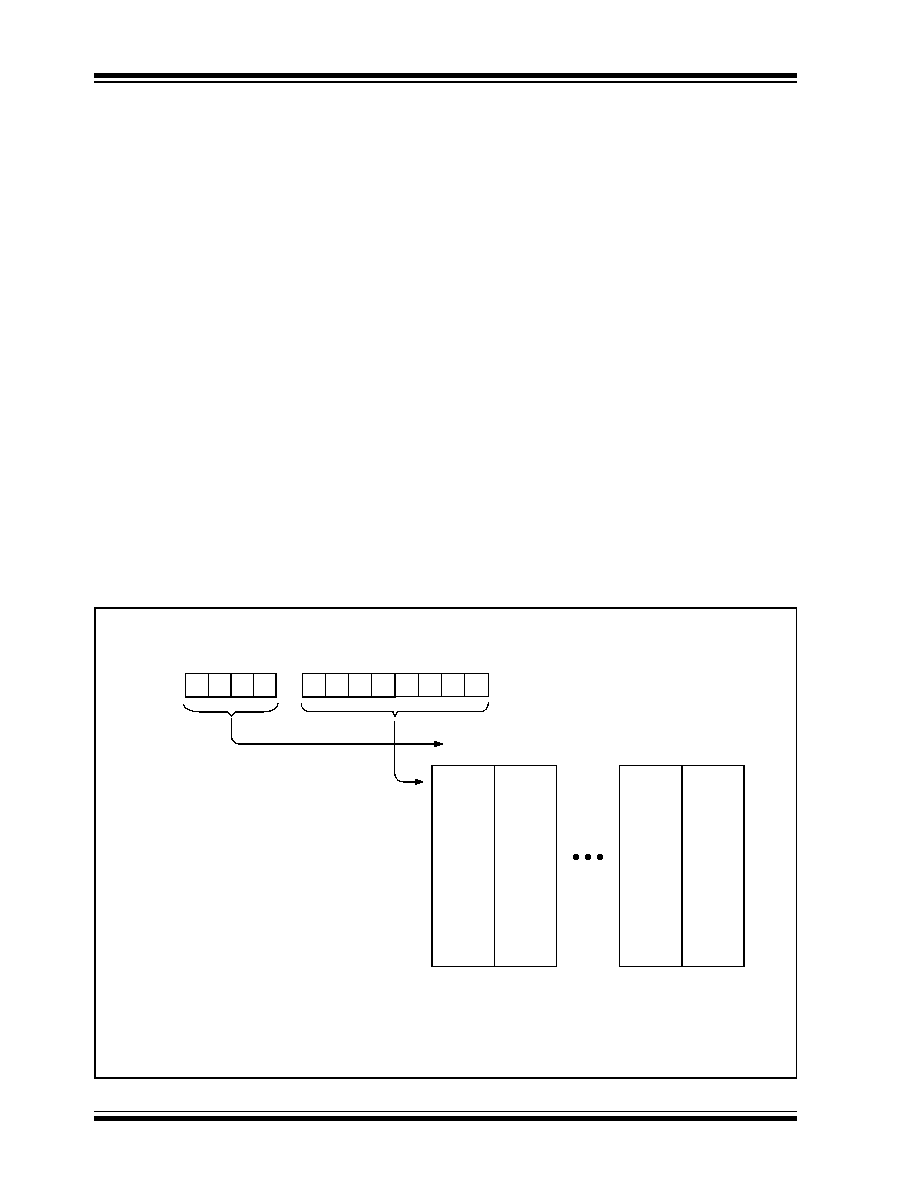
PIC18FXX8
DS41159B-page 54
Preliminary
2002 Microchip Technology Inc.
4.10
Access Bank
The Access Bank is an architectural enhancement that
is very useful for C compiler code optimization. The
techniques used by the C compiler are also useful for
programs written in assembly.
This data memory region can be used for:
� Intermediate computational values
� Local variables of subroutines
� Faster context saving/switching of variables
� Common variables
� Faster evaluation/control of SFRs (no banking)
The Access Bank is comprised of the upper 160 bytes
in Bank 15 (SFRs) and the lower 96 bytes in Bank 0.
These two sections will be referred to as Access Bank
High and Access Bank Low, respectively. Figure 4-6
indicates the Access Bank areas.
A bit in the instruction word specifies if the operation is
to occur in the bank specified by the BSR register, or in
the Access Bank.
When forced in the Access Bank (a = '
0
'), the last
address in Access Bank Low is followed by the first
address in Access Bank High. Access Bank High maps
most of the Special Function Registers so that these
registers can be accessed without any software
overhead.
4.11
Bank Select Register (BSR)
The need for a large general purpose memory space
dictates a RAM banking scheme. The data memory is
partitioned into sixteen banks. When using direct
addressing, the BSR should be configured for the
desired bank.
BSR<3:0> holds the upper 4 bits of the 12-bit RAM
address. The BSR<7:4> bits will always read '
0
's, and
writes will have no effect.
A
MOVLB
instruction has been provided in the
instruction set to assist in selecting banks.
If the currently selected bank is not implemented, any
read will return all '
0
's and all writes are ignored. The
STATUS register bits will be set/cleared as appropriate
for the instruction performed.
Each Bank extends up to FFh (256 bytes). All data
memory is implemented as static RAM.
A
MOVFF
instruction ignores the BSR, since the 12-bit
addresses are embedded into the instruction word.
Section 4.12 provides a description of indirect address-
ing, which allows linear addressing of the entire RAM
space.
FIGURE 4-7:
DIRECT ADDRESSING
Note
1: For register file map detail, see Table 4-1.
2: The access bit of the instruction can be used to force an override of the selected bank (BSR<3:0>) to the
registers of the Access Bank.
3: The
MOVFF
instruction embeds the entire 12-bit address in the instruction.
Data
Memory
(1)
Direct Addressing
Bank Select
(2)
Location Select
(3)
BSR<3:0>
7
0
From Opcode
(3)
00h
01h
0Eh
0Fh
Bank 0
Bank 1
Bank 14
Bank 15
1FFh
100h
0FFh
000h
EFFh
E00h
FFFh
F00h

2002 Microchip Technology Inc.
Preliminary
DS41159B-page 55
PIC18FXX8
4.12
Indirect Addressing, INDF and
FSR Registers
Indirect addressing is a mode of addressing data mem-
ory, where the data memory address in the instruction
is not fixed. A SFR register is used as a pointer to the
data memory location that is to be read or written. Since
this pointer is in RAM, the contents can be modified by
the program. This can be useful for data tables in the
data memory and for software stacks. Figure 4-8
shows the operation of indirect addressing. This shows
the moving of the value to the data memory address
specified by the value of the FSR register.
Indirect addressing is possible by using one of the INDF
registers. Any instruction using the INDF register actually
accesses the register indicated by the File Select Regis-
ter, FSR. Reading the INDF register itself, indirectly (FSR
= '
0
'), will read 00h. Writing to the INDF register indirectly,
results in a no operation. The FSR register contains a
12-bit address, which is shown in Figure 4-8.
The INDFn (0
n
2) register is not a physical register.
Addressing INDFn actually addresses the register
whose address is contained in the FSRn register
(FSRn is a pointer). This is indirect addressing.
Example 4-5 shows a simple use of indirect addressing
to clear the RAM in Bank 1 (locations 100h-1FFh) in a
minimum number of instructions.
EXAMPLE 4-5:
HOW TO CLEAR RAM
(BANK 1) USING
INDIRECT ADDRESSING
There are three indirect addressing registers. To
address the entire data memory space (4096 bytes),
these registers are 12-bits wide. To store the 12 bits of
addressing information, two 8-bit registers are
required. These indirect addressing registers are:
1.
FSR0: composed of FSR0H:FSR0L
2.
FSR1: composed of FSR1H:FSR1L
3.
FSR2: composed of FSR2H:FSR2L
In addition, there are registers INDF0, INDF1 and
INDF2, which are not physically implemented. Reading
or writing to these registers activates indirect address-
ing, with the value in the corresponding FSR register
being the address of the data.
If an instruction writes a value to INDF0, the value will
be written to the address indicated by FSR0H:FSR0L.
A read from INDF1 reads the data from the address
indicated by FSR1H:FSR1L. INDFn can be used in
code anywhere an operand can be used.
If INDF0, INDF1 or INDF2 are read indirectly via an
FSR, all '
0
's are read (zero bit is set). Similarly, if
INDF0, INDF1 or INDF2 are written to indirectly, the
operation will be equivalent to a
NOP
instruction and the
STATUS bits are not affected.
4.12.1
INDIRECT ADDRESSING
OPERATION
Each FSR register has an INDF register associated with
it, plus four additional register addresses. Performing an
operation on one of these five registers determines how
the FSR will be modified during indirect addressing.
� When data access is done to one of the five
INDFn locations, the address selected will
configure the FSRn register to:
- Do nothing to FSRn after an indirect access
(no change) - INDFn
- Auto-decrement FSRn after an indirect
access (post-decrement) - POSTDECn
- Auto-increment FSRn after an indirect
access (post-increment) - POSTINCn
- Auto-increment FSRn before an indirect
access (pre-increment) - PREINCn
- Use the value in the WREG register as an off-
set to FSRn. Do not modify the value of the
WREG or the FSRn register after an indirect
access (no change) - PLUSWn
When using the auto-increment or auto-decrement fea-
tures, the effect on the FSR is not reflected in the
STATUS register. For example, if the indirect address
causes the FSR to equal '0', the Z bit will not be set.
Incrementing or decrementing an FSR affects all 12
bits. That is, when FSRnL overflows from an increment,
FSRnH will be incremented automatically.
Adding these features allows the FSRn to be used as a
software stack pointer, in addition to its uses for table
operations in data memory.
Each FSR has an address associated with it that per-
forms an indexed indirect access. When a data access to
this INDFn location (PLUSWn) occurs, the FSRn is con-
figured to add the 2's complement value in the WREG
register and the value in FSR to form the address before
an indirect access. The FSR value is not changed.
If an FSR register contains a value that indicates one of
the INDFn, an indirect read will read 00h (zero bit is
set), while an indirect write will be equivalent to a
NOP
(STATUS bits are not affected).
If an indirect addressing operation is done where the
target address is an FSRnH or FSRnL register, the
write operation will dominate over the pre- or post-
increment/decrement functions.
LFSR
FSR0, 100h ;
NEXT
CLRF
POSTINC0
; Clear INDF
; register
; & inc pointer
BTFSS
FSR0H, 1
; All done
; w/ Bank1?
BRA
NEXT
; NO, clear next
CONTINUE
;
: ;
YES,
continue
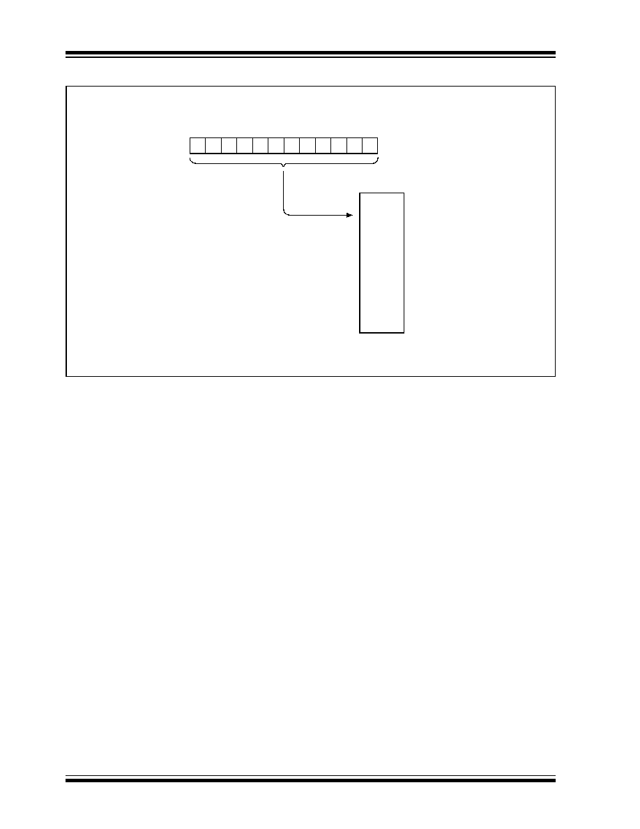
PIC18FXX8
DS41159B-page 56
Preliminary
2002 Microchip Technology Inc.
FIGURE 4-8:
INDIRECT ADDRESSING
Note
1: For register file map detail, see Table 4-1.
Data
Memory
(1)
Indirect Addressing
FSR Register
11
8
7
0
0FFFh
0000h
Location Select
FSRnH
FSRnL
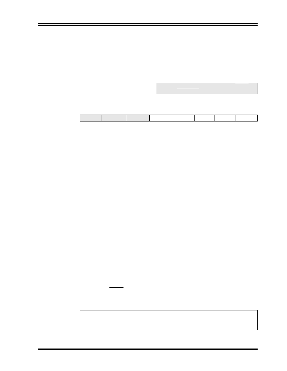
2002 Microchip Technology Inc.
Preliminary
DS41159B-page 57
PIC18FXX8
4.13
STATUS Register
The STATUS register, shown in Register 4-2, contains
the arithmetic status of the ALU. The STATUS register
can be the destination for any instruction, as with any
other register. If the STATUS register is the destination
for an instruction that affects the Z, DC, C, OV, or N bits,
then the write to these five bits is disabled. These bits
are set or cleared according to the device logic. There-
fore, the result of an instruction with the STATUS
register as destination may be different than intended.
For example,
CLRF STATUS
will clear the upper three
bits and set the Z bit. This leaves the STATUS register
as
000u u1uu
(where
u
= unchanged).
It is recommended, therefore, that only
BCF, BSF,
SWAPF, MOVFF
and
MOVWF
instructions are used to
alter the STATUS register, because these instructions
do not affect the Z, C, DC, OV, or N bits from the
STATUS register. For other instructions which do not
affect the status bits, see Table 25-2.
REGISTER 4-2:
STATUS REGISTER
Note:
The C and DC bits operate as a borrow and
digit borrow bit respectively, in subtraction.
U-0
U-0
U-0
R/W-x
R/W-x
R/W-x
R/W-x
R/W-x
--
--
--
N
OV
Z
DC
C
bit 7
bit 0
bit 7-5
Unimplemented: Read as '0'
bit 4
N: Negative bit
This bit is used for signed arithmetic (2's complement). It indicates whether the result of the ALU
operation was negative (ALU MSb = 1).
1
= Result was negative
0
= Result was positive
bit 3
OV: Overflow bit
This bit is used for signed arithmetic (2's complement). It indicates an overflow of the 7-bit
magnitude, which causes the sign bit (bit 7) to change state.
1
= Overflow occurred for signed arithmetic (in this arithmetic operation)
0
= No overflow occurred
bit 2
Z: Zero bit
1
= The result of an arithmetic or logic operation is zero
0
= The result of an arithmetic or logic operation is not zero
bit 1
DC: Digit carry/borrow bit
For
ADDWF, ADDLW, SUBLW,
and
SUBWF
instructions
1
= A carry-out from the 4th low order bit of the result occurred
0
= No carry-out from the 4th low order bit of the result
Note:
For borrow, the polarity is reversed. A subtraction is executed by adding the 2's com-
plement of the second operand. For rotate (
RRCF, RRNCF, RLCF,
and
RLNCF
)
instructions, this bit is loaded with either the bit 4 or bit 3 of the source register.
bit 0
C: Carry/borrow bit
For
ADDWF, ADDLW, SUBLW,
and
SUBWF
instructions
1
= A carry-out from the Most Significant bit of the result occurred
0
= No carry-out from the Most Significant bit of the result occurred
Note:
For borrow, the polarity is reversed. A subtraction is executed by adding the 2's com-
plement of the second operand. For rotate (
RRF, RLF
) instructions, this bit is
loaded with either the high or low order bit of the source register.
Legend:
R = Readable bit
W = Writable bit
U = Unimplemented bit, read as `0'
- n = Value at POR
'1' = Bit is set
'0' = Bit is cleared
x = Bit is unknown
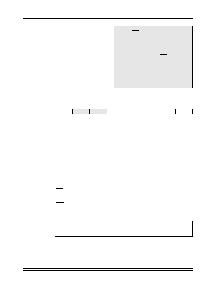
PIC18FXX8
DS41159B-page 58
Preliminary
2002 Microchip Technology Inc.
4.14
RCON Register
The Reset Control (RCON) register contains flag bits
that allow differentiation between the sources of a
device RESET. These flags include the TO, PD, POR,
BOR and RI bits. This register is readable and writable.
REGISTER 4-3:
RCON REGISTER
Note 1: If the BOREN configuration bit is set,
BOR is '1' on Power-on Reset. If the
BOREN configuration bit is clear, BOR is
unknown on Power-on Reset.
The BOR status bit is a "don't care" and is
not necessarily predictable if the brown-
out circuit is disabled (the BOREN config-
uration bit is clear). BOR must then be set
by the user and checked on subsequent
RESETS to see if it is clear, indicating a
brown-out has occurred.
2: It is recommended that the POR bit be set
after a Power-on Reset has been
detected, so that subsequent Power-on
Resets may be detected.
R/W-0
U-0
U-0
R/W-1
R-1
R-1
R/W-0
R/W-0
IPEN
--
--
RI
TO
PD
POR
BOR
bit 7
bit 0
bit 7
IPEN: Interrupt Priority Enable bit
1
= Enable priority levels on interrupts
0
= Disable priority levels on interrupts (16CXXX Compatibility mode)
bit 6-5
Unimplemented: Read as '0'
bit 4
RI:
RESET
Instruction Flag bit
1
= The
RESET
instruction was not executed
0
= The
RESET
instruction was executed causing a device RESET
(must be set in software after a Brown-out Reset occurs)
bit 3
TO: Watchdog Time-out Flag bit
1
= After power-up,
CLRWDT
instruction, or
SLEEP
instruction
0
= A WDT time-out occurred
bit 2
PD: Power-down Detection Flag bit
1
= After power-up or by the
CLRWDT
instruction
0
= By execution of the
SLEEP
instruction
bit 1
POR: Power-on Reset Status bit
1
= A Power-on Reset has not occurred
0
= A Power-on Reset occurred (must be set in software after a Power-on Reset occurs)
bit 0
BOR: Brown-out Reset Status bit
1
= A Brown-out Reset has not occurred
0
= A Brown-out Reset occurred (must be set in software after a Brown-out Reset occurs)
Legend:
R = Readable bit
W = Writable bit
U = Unimplemented bit, read as `0'
- n = Value at POR
'1' = Bit is set
'0' = Bit is cleared
x = Bit is unknown

2002 Microchip Technology Inc.
Preliminary
DS41159B-page 59
PIC18FXX8
5.0
DATA EEPROM MEMORY
The Data EEPROM is readable and writable during
normal operation over the entire V
DD
range. The data
memory is not directly mapped in the register file
space. Instead, it is indirectly addressed through the
Special Function Registers (SFR).
There are four SFRs used to read and write the
program and data EEPROM memory. These registers
are:
� EECON1
� EECON2
� EEDATA
� EEADR
The EEPROM data memory allows byte read and write.
When interfacing to the data memory block, EEDATA
holds the 8-bit data for read/write and EEADR holds the
address of the EEPROM location being accessed. The
PIC18FXX8 devices have 256 bytes of data EEPROM,
with an address range from 00h to FFh.
The EEPROM data memory is rated for high erase/
write cycles. A byte write automatically erases the loca-
tion and writes the new data (erase-before-write). The
write time is controlled by an on-chip timer. The write
time will vary with voltage and temperature, as well as
from chip-to-chip. Please refer to the specifications for
exact limits.
5.1
EEADR Register
The address register can address up to a maximum of
256 bytes of data EEPROM.
5.2
EECON1 and EECON2 Registers
EECON1 is the control register for EEPROM memory
accesses.
EECON2 is not a physical register. Reading EECON2
will read all '
0
's. The EECON2 register is used
exclusively in the EEPROM write sequence.
Control bits RD and WR initiate read and write opera-
tions, respectively. These bits cannot be cleared, only
set, in software. They are cleared in hardware at the
completion of the read or write operation. The inability
to clear the WR bit in software prevents the accidental
or premature termination of a write operation.
The WREN bit, when set, will allow a write operation.
On power-up, the WREN bit is clear. The WRERR bit is
set when a write operation is interrupted by a MCLR
Reset, or a WDT Time-out Reset, during normal oper-
ation. In these situations, following RESET, the user
can check the WRERR bit and rewrite the location. The
data and address registers (EEDATA and EEADR)
remain unchanged.
Note:
Interrupt flag bit EEIF in the PIR2 register
is set when write is complete. It must be
cleared in software.

PIC18FXX8
DS41159B-page 60
Preliminary
2002 Microchip Technology Inc.
REGISTER 5-1:
EECON1 REGISTER
R/W-x
R/W-x
U-0
R/W-0
R/W-x
R/W-0
R/S-0
R/S-0
EEPGD
CFGS
--
FREE
WRERR
WREN
WR
RD
bit 7
bit 0
bit 7
EEPGD: FLASH Program or Data EEPROM Memory Select bit
1
= Access program FLASH memory
0
= Access data EEPROM memory
bit 6
CFGS: FLASH Program/Data EE or Configuration Select bit
1
= Access configuration registers
0
= Access program FLASH or data EEPROM memory
bit 5
Unimplemented: Read as '0'
bit 4
FREE: FLASH Row Erase Enable bit
1
= Erase the program memory row addressed by TBLPTR on the next WR command
(reset by hardware)
0
= Perform write only
bit 3
WRERR: Write Error Flag bit
1
= A write operation is prematurely terminated
(any MCLR or any WDT Reset during self-timed programming in normal operation)
0
= The write operation completed
Note:
When a WRERR occurs, the EEPGD or FREE bits are not cleared. This allows tracing
of the error condition.
bit 2
WREN: Write Enable bit
1
= Allows write cycles
0
= Inhibits write to the EEPROM or FLASH memory
bit 1
WR: Write Control bit
1
= Initiates a data EEPROM erase/write cycle or a program memory erase cycle or write cycle
(The operation is self-timed and the bit is cleared by hardware once write is complete. The
WR bit can only be set (not cleared) in software.)
0
= Write cycle is complete
bit 0
RD: Read Control bit
1
= Initiates an EEPROM read
(Read takes one cycle. RD is cleared in hardware. The RD bit can only be set (not cleared)
in software. RD bit cannot be set when EEPGD = 1.)
0
= Does not initiate an EEPROM read
Legend:
R = Readable bit
W = Writable bit
U = Unimplemented bit, read as `0'
- n = Value at POR
'1' = Bit is set
'0' = Bit is cleared
x = Bit is unknown

2002 Microchip Technology Inc.
Preliminary
DS41159B-page 61
PIC18FXX8
5.3
Reading the Data EEPROM
Memory
To read a data memory location, the user must write the
address to the EEADR register, clear the EEPGD and
CFGS control bits (EECON1<7:6>) and then set con-
trol bit RD (EECON1<0>). The data is available in the
very next instruction cycle of the EEDATA register;
therefore, it can be read by the next instruction.
EEDATA will hold this value until another read opera-
tion, or until it is written to by the user (during a write
operation).
EXAMPLE 5-1:
DATA EEPROM READ
5.4
Writing to the Data EEPROM
Memory
To write an EEPROM data location, the address must
first be written to the EEADR register and the data writ-
ten to the EEDATA register. Then, the sequence in
Example 5-2 must be followed to initiate the write cycle.
The write will not initiate if the above sequence is not
exactly followed (write 55h to EECON2, write 0AAh to
EECON2, then set WR bit) for each byte. It is strongly
recommended that interrupts be disabled during this
code segment.
Additionally, the WREN bit in EECON1 must be set to
enable writes. This mechanism prevents accidental
writes to data EEPROM due to unexpected code exe-
cution (i.e., runaway programs). The WREN bit should
be kept clear at all times, except when updating the
EEPROM. The WREN bit is not cleared by hardware.
After a write sequence has been initiated, clearing the
WREN bit will not affect the current write cycle. The WR
bit will be inhibited from being set unless the WREN bit
is set. The WREN bit must be set on a previous instruc-
tion. Both WR and WREN cannot be set with the same
instruction.
At the completion of the write cycle, the WR bit is
cleared in hardware and the EEPROM Write Complete
Interrupt Flag bit (EEIF) is set. The user may either
enable this interrupt, or roll this bit. EEIF must be
cleared by software.
EXAMPLE 5-2:
DATA EEPROM WRITE
MOVLW
DATA_EE_ADDR
;
MOVWF
EEADR
;Data Memory Address
;to read
BCF
EECON1, EEPGD
;Point to DATA memory
BCS
EECON1, CFGS
;
BSF
EECON1, RD
;EEPROM Read
MOVF
EEDATA, W
;W = EEDATA
MOVLW
DATA_EE_ADDR
;
MOVWF
EEADR
; Data Memory Address to write
MOVLW
DATA_EE_DATA
;
MOVWF
EEDATA
; Data Memory Value to write
BCF
EECON1, EEPGD
; Point to DATA memory
BCS
EECON1, CFGS
;
BSF
EECON1, WREN
; Enable writes
BCF
INTCON, GIE
; Disable Interrupts
MOVLW
55h
;
Required
MOVWF
EECON2
; Write 55h
Sequence
MOVLW
0AAh
;
MOVWF
EECON2
; Write 0AAh
BSF
EECON1, WR
; Set WR bit to begin write
BSF
INTCON, GIE
; Enable Interrupts
; User code execution
BCF
EECON1, WREN
; Disable writes

PIC18FXX8
DS41159B-page 62
Preliminary
2002 Microchip Technology Inc.
5.5
Write Verify
Depending on the application, good programming
practice may dictate that the value written to the mem-
ory should be verified against the original value. This
should be used in applications where excessive writes
can stress bits near the specification limit.
Generally, a write failure will be a bit which was written
as a '
1
', but reads back as a '
0
' (due to leakage off the
cell).
5.6
Protection Against Spurious Write
There are conditions when the device may not want to
write to the data EEPROM memory. To protect against
spurious EEPROM writes, various mechanisms have
been built-in. On power-up, the WREN bit is cleared.
Also, the Power-up Timer (72 ms duration) prevents
EEPROM write.
The write initiate sequence and the WREN bit together
reduce the probability of an accidental write during
brown-out, power glitch, or software malfunction.
5.7
Operation During Code Protect
Data EEPROM memory has its own code protect
mechanism. External read and write operations are
disabled if either of these mechanisms are enabled.
The microcontroller itself can both read and write to the
internal data EEPROM, regardless of the state of the
code protect configuration bit. Refer to Section 24.0,
Special Features of the CPU for additional information.
5.8
Using the Data EEPROM
The data EEPROM is a high-endurance, byte address-
able array that has been optimized for the storage of
frequently changing information (e.g., program vari-
ables or other data that are updated often). Frequently
changing values will typically be updated more often
than specification D124 or D124A. If this is not the
case, an array refresh must be performed. For this rea-
son, variables that change infrequently (such as con-
stants, IDs, calibration, etc.) should be stored in FLASH
program memory. A simple data EEPROM refresh
routine is shown in Example 5-3.
EXAMPLE 5-3:
DATA EEPROM REFRESH ROUTINE
Note:
If Data EEPROM is only used to store con-
stants and/or data that changes rarely, an
array refresh is likely not required. See
specification D124 or D124A.
clrf
EEADR
; Start at address 0
bcf
EECON1,CFGS
; Set for memory
bcf
EECON1,EEPGD
; Set for Data EEPROM
bcf
INTCON,GIE
; Disable interrupts
bsf
EECON1,WREN
; Enable writes
Loop
; Loop to refresh array
bsf
EECON1,RD
; Read current address
movlw
55h
;
movwf
EECON2
; Write 55h
movlw
AAh
;
movwf
EECON2
; Write AAh
bsf
EECON1,WR
; Set WR bit to begin write
btfsc
EECON1,WR
; Wait for write to complete
bra
$-2
incfsz
EEADR,F
; Increment address
bra
Loop
; Not zero, do it again
bcf
EECON1,WREN
; Disable writes
bsf
INTCON,GIE
; Enable interrupts
2002 Microchip Technology Inc.
Preliminary
DS41159B-page 63
PIC18FXX8
TABLE 5-1:
REGISTERS ASSOCIATED WITH DATA EEPROM MEMORY
Name
Bit 7
Bit 6
Bit 5
Bit 4
Bit 3
Bit 2
Bit 1
Bit 0
Value on:
POR, BOR
Value on
all other
RESETS
INTCON
GIE/GIEH PEIE/GIEL
TMR0IE
INT0IE
RBIE
TMR0IF
INT0IF
RBIF
0000 000x
0000 000u
EEADR
EEPROM Address Register
xxxx xxxx
uuuu uuuu
EEDATA
EEPROM Data Register
xxxx xxxx
uuuu uuuu
EECON2
EEPROM Control Register2 (not a physical register)
--
--
EECON1
EEPGD
CFGS
--
FREE
WRERR
WREN
WR
RD
xx-0 x000
uu-0 u000
IPR2
--
CMIP
--
EEIP
BCLIP
LVDIP
TMR3IP
ECCP1IP
-1-1 1111
-1-1 1111
PIR2
--
CMIF
--
EEIF
BCLIF
LVDIF
TMR3IF
ECCP1IF
-0-0 0000
-0-0 0000
PIE2
--
CMIE
--
EEIE
BCLIE
LVDIE
TMR3IE
ECCP1IE
-0-0 0000
-0-0 0000
Legend:
x
= unknown,
u
= unchanged, r = reserved,
-
= unimplemented, read as '0'.
Shaded cells are not used during FLASH/EEPROM access.

PIC18FXX8
DS41159B-page 64
Preliminary
2002 Microchip Technology Inc.
NOTES:
2002 Microchip Technology Inc.
Preliminary
DS41159B-page 65
PIC18FXX8
6.0
FLASH PROGRAM MEMORY
The FLASH Program Memory is readable, writable,
and erasable during normal operation over the entire
V
DD
range.
A read from program memory is executed on one byte
at a time. A write to program memory is executed on
blocks of 8 bytes at a time. Program memory is erased
in blocks of 64 bytes at a time. A bulk erase operation
may not be issued from user code.
Writing or erasing program memory will cease instruc-
tion fetches until the operation is complete. The pro-
gram memory cannot be accessed during the write or
erase, therefore, code cannot execute. An internal pro-
gramming timer terminates program memory writes
and erases.
A value written to program memory does not need to be
a valid instruction. Executing a program memory
location that forms an invalid instruction results in a
NOP
.
6.1
Table Reads and Table Writes
In order to read and write program memory, there are
two operations that allow the processor to move bytes
between the program memory space and the data
RAM:
� Table Read (
TBLRD
)
� Table Write (
TBLWT
)
The program memory space is 16-bits wide, while the
data RAM space is 8-bits wide. Table Reads and Table
Writes move data between these two memory spaces
through an 8-bit register (TABLAT).
Table Read operations retrieve data from program
memory and places it into the data RAM space.
Figure 6-1 shows the operation of a Table Read with
program memory and data RAM.
Table Write operations store data from the data mem-
ory space into holding registers in program memory.
The procedure to write the contents of the holding reg-
isters into program memory is detailed in Section 6.5,
Writing to FLASH Program Memory. Figure 6-2 shows
the operation of a Table Write with program memory
and data RAM.
Table operations work with byte entities. A table block
containing data, rather than program instructions, is not
required to be word aligned. Therefore, a table block
can start and end at any byte address. If a Table Write
is being used to write executable code into program
memory, program instructions will need to be word
aligned.
FIGURE 6-1:
TABLE READ OPERATION
Table Pointer
(1)
Table Latch (8-bit)
Program Memory
TBLPTRH
TBLPTRL
TABLAT
TBLPTRU
Instruction:
TBLRD
*
Note
1: Table Pointer points to a byte in program memory.
Program Memory
(TBLPTR)
PIC18FXX8
DS41159B-page 66
Preliminary
2002 Microchip Technology Inc.
FIGURE 6-2:
TABLE WRITE OPERATION
6.2
Control Registers
Several control registers are used in conjunction with
the
TBLRD
and
TBLWT
instructions. These include the:
� EECON1 register
� EECON2 register
� TABLAT register
� TBLPTR registers
6.2.1
EECON1 AND EECON2 REGISTERS
EECON1 is the control register for memory accesses.
EECON2 is not a physical register. Reading EECON2
will read all '
0
's. The EECON2 register is used
exclusively in the memory write and erase sequences.
Control bit EEPGD determines if the access will be a
program or data EEPROM memory access. When
clear, any subsequent operations will operate on the
data EEPROM memory. When set, any subsequent
operations will operate on the program memory.
Control bit CFGS determines if the access will be to the
configuration/calibration registers or to program
memory/data EEPROM memory. When set, subse-
quent operations will operate on configuration regis-
ters, regardless of EEPGD (see Section 24.0, Special
Features of the CPU). When clear, memory selection
access is determined by EEPGD.
The FREE bit, when set, will allow a program memory
erase operation. When the FREE bit is set, the erase
operation is initiated on the next WR command. When
FREE is clear, only writes are enabled.
The WREN bit, when set, will allow a write operation.
On power-up, the WREN bit is clear. The WRERR bit is
set when a write operation is interrupted by a MCLR
Reset or a WDT Time-out Reset during normal opera-
tion. In these situations, the user can check the
WRERR bit and rewrite the location. It is necessary to
reload the data and address registers (EEDATA and
EEADR), due to RESET values of zero.
Control bits RD and WR initiate read and write opera-
tions, respectively. These bits cannot be cleared, only
set, in software. They are cleared in hardware at the
completion of the read or write operation. The inability
to clear the WR bit in software prevents the accidental
or premature termination of a write operation. The RD
bit cannot be set when accessing program memory
(EEPGD = 1).
Table Pointer
(1)
Table Latch (8-bit)
TBLPTRH
TBLPTRL
TABLAT
Program Memory
(TBLPTR)
TBLPTRU
Instruction:
TBLWT
*
Note
1: Table Pointer actually points to one of eight holding registers, the address of which is determined by TBLPTRL<2:0>.
The process for physically writing data to the Program Memory Array is discussed in Section 6.5.
Holding Registers
Program Memory
Note:
If interrupts are enabled before the WR
command, interrupt flag bit EEIF in the
PIR2 register, is set when the write is com-
plete. It must be cleared in software. This
interrupt is not required to determine the
end of a FLASH program memory write
cycle.

2002 Microchip Technology Inc.
Preliminary
DS41159B-page 67
PIC18FXX8
REGISTER 6-1:
EECON1 REGISTER
R/W-x
R/W-x
U-0
R/W-0
R/W-x
R/W-0
R/S-0
R/S-0
EEPGD
CFGS
--
FREE
WRERR
WREN
WR
RD
bit 7
bit 0
bit 7
EEPGD: FLASH Program or Data EEPROM Memory Select bit
1
= Access program FLASH memory
0
= Access data EEPROM memory
bit 6
CFGS: FLASH Program/Data EE or Configuration Select bit
1
= Access configuration registers
0
= Access program FLASH or data EEPROM memory
bit 5
Unimplemented: Read as '0'
bit 4
FREE: FLASH Row Erase Enable bit
1
= Erase the program memory row addressed by TBLPTR on the next WR command
(cleared by completion of erase operation)
0
= Perform write only
bit 3
WRERR: Write Error Flag bit
1
= A write operation is prematurely terminated
(any MCLR or any WDT Reset during self-timed programming in normal operation)
0
= The write operation completed
Note:
When a WRERR occurs, the EEPGD and CFGS bits are not cleared. This allows
tracing of the error condition.
bit 2
WREN: Write Enable bit
1
= Allows write cycles
0
= Inhibits write to the EEPROM or FLASH memory
bit 1
WR: Write Control bit
1
= Initiates a data EEPROM erase/write cycle or a program memory erase cycle or write cycle.
(The operation is self timed and the bit is cleared by hardware once write is complete. The
WR bit can only be set (not cleared) in software.)
0
= Write cycle to the EEPROM is complete
bit 0
RD: Read Control bit
1
= Initiates an EEPROM read
(Read takes one cycle. RD is cleared in hardware. The RD bit can only be set (not cleared)
in software. RD bit cannot be set when EEPGD = 1.)
0
= Does not initiate an EEPROM read
Legend:
R = Readable bit
W = Writable bit
U = Unimplemented bit, read as `0'
- n = Value at POR
'1' = Bit is set
'0' = Bit is cleared
x = Bit is unknown
PIC18FXX8
DS41159B-page 68
Preliminary
2002 Microchip Technology Inc.
6.2.2
TABLAT - TABLE LATCH REGISTER
The Table Latch (TABLAT) is an 8-bit register mapped
into the SFR space. The Table Latch is used to hold
8-bit data during data transfers between program
memory and data RAM.
6.2.3
TBLPTR - TABLE POINTER
REGISTER
The Table Pointer (TBLPTR) addresses a byte within
the program memory. The TBLPTR is comprised of
three SFR registers: Table Pointer Upper Byte, Table
Pointer High Byte and Table Pointer Low Byte
(TBLPTRU:TBLPTRH:TBLPTRL). These three regis-
ters join to form a 22-bit wide pointer. The low order 21
bits allow the device to address up to 2 Mbytes of pro-
gram memory space. The 22nd bit allows access to the
Device ID, the User ID and the Configuration bits.
The table pointer, TBLPTR, is used by the
TBLRD
and
TBLWT
instructions. These instructions can update the
TBLPTR in one of four ways, based on the table oper-
ation. These operations are shown in Table 6-1. These
operations on the TBLPTR only affect the low order 21
bits.
6.2.4
TABLE POINTER BOUNDARIES
TBLPTR is used in reads, writes, and erases of the
FLASH program memory.
When a
TBLRD
is executed, all 22 bits of the Table
Pointer determine which byte is read from program
memory into TABLAT.
When a
TBLWT
is executed, the three LSbs of the Table
Pointer (TBLPTR<2:0>) determine which of the eight
program memory holding registers is written to. When
the timed write to program memory (long write) begins,
the 19 MSbs of the Table Pointer, TBLPTR
(TBLPTR<21:3>), will determine which program mem-
ory block of 8 bytes is written to. For more detail, see
Section 6.5,Writing to FLASH Program Memory.
When an erase of program memory is executed, the 16
MSbs of the Table Pointer (TBLPTR<21:6>) point to the
64-byte block that will be erased. The Least Significant
bits (TBLPTR<5:0>) are ignored.
Figure 6-3 describes the relevant boundaries of
TBLPTR based on FLASH program memory
operations.
TABLE 6-1:
TABLE POINTER OPERATIONS WITH
TBLRD
AND
TBLWT
INSTRUCTIONS
FIGURE 6-3:
TABLE POINTER BOUNDARIES BASED ON OPERATION
Example
Operation on Table Pointer
TBLRD*
TBLWT*
TBLPTR is not modified
TBLRD*+
TBLWT*+
TBLPTR is incremented after the read/write
TBLRD*-
TBLWT*-
TBLPTR is decremented after the read/write
TBLRD+*
TBLWT+*
TBLPTR is incremented before the read/write
21
16
15
8
7
0
ERASE - TBLPTR<21:6>
WRITE - TBLPTR<21:3>
READ - TBLPTR<21:0>
TBLPTRL
TBLPTRH
TBLPTRU
2002 Microchip Technology Inc.
Preliminary
DS41159B-page 69
PIC18FXX8
6.3
Reading the FLASH Program
Memory
The
TBLRD
instruction is used to retrieve data from pro-
gram memory and place into data RAM. Table Reads
from program memory are performed one byte at a
time.
TBLPTR points to a byte address in program space.
Executing
TBLRD
places the byte pointed to into
TABLAT. In addition, TBLPTR can be modified
automatically for the next Table Read operation.
The internal program memory is typically organized by
words. The Least Significant bit of the address selects
between the high and low bytes of the word. Figure 6-4
shows the interface between the internal program
memory and the TABLAT.
FIGURE 6-4:
READS FROM FLASH PROGRAM MEMORY
EXAMPLE 6-1:
READING A FLASH PROGRAM MEMORY WORD
(Even Byte Address)
Program Memory
(Odd Byte Address)
TBLRD
TABLAT
TBLPTR
= xxxxx1
FETCH
Instruction Register
(IR)
Read Register
TBLPTR
= xxxxx0
MOVLW CODE_ADDR_UPPER
; Load TBLPTR with the base
MOVWF TBLPTRU
; address of the word
MOVLW CODE_ADDR_HIGH
MOVWF TBLPTRH
MOVLW CODE_ADDR_LOW
MOVWF TBLPTRL
READ_WORD
TBLRD*+
; read into TABLAT and increment
MOVF TABLAT, W
; get data
MOVWF WORD_LSB
TBLRD*+
; read into TABLAT and increment
MOVF TABLAT, W
; get data
MOVWF WORD_MSB

PIC18FXX8
DS41159B-page 70
Preliminary
2002 Microchip Technology Inc.
6.4
Erasing FLASH Program memory
The minimum erase block is 32 words or 64 bytes. Only
through the use of an external programmer, or through
ICSP control, can larger blocks of program memory be
bulk erased. Word erase in the FLASH array is not
supported.
When initiating an erase sequence from the micro-
controller itself, a block of 64 bytes of program memory
is erased. The Most Significant 16 bits of the
TBLPTR<21:6> point to the block being erased.
TBLPTR<5:0> are ignored.
The EECON1 register commands the erase operation.
The EEPGD bit must be set to point to the FLASH pro-
gram memory. The WREN bit must be set to enable
write operations. The FREE bit is set to select an erase
operation.
For protection, the write initiate sequence for EECON2
must be used.
A long write is necessary for erasing the internal
FLASH. Instruction execution is halted while in a long
write cycle. The long write will be terminated by the
internal programming timer.
6.4.1
FLASH PROGRAM MEMORY
ERASE SEQUENCE
The sequence of events for erasing a block of internal
program memory location is:
1.
Load table pointer with address of row being
erased.
2.
Set the EECON1 register for the erase operation:
� set the EEPGD bit to point to program memory;
� clear the CFGS bit to access program memory;
� set the WREN bit to enable writes;
� set the FREE bit to enable the erase.
3.
Disable interrupts.
4.
Write 55h to EECON2.
5.
Write 0AAh to EECON2.
6.
Set the WR bit. This will begin the row erase
cycle.
7.
The CPU will stall for duration of the erase
(about 2 ms using internal timer).
8.
Execute a
NOP
.
9.
Re-enable interrupts.
EXAMPLE 6-2:
ERASING A FLASH PROGRAM MEMORY ROW
Note:
A
NOP
is needed after the WR command to
ensure proper code execution.
MOVLW
upper (CODE_ADDR)
; load TBLPTR with the base
MOVWF
TBLPTRU
; address of the memory block
MOVLW
high (CODE_ADDR)
MOVWF
TBLPTRH
MOVLW
low (CODE_ADDR)
MOVWF
TBLPTRL
ERASE_ROW
BSF
EECON1,EEPGD
; point to FLASH program memory
BCF
EECON1,CFGS
; access FLASH program memory
BSF
EECON1,WREN
; enable write to memory
BSF
EECON1,FREE
; enable Row Erase operation
BCF
INTCON,GIE
; disable interrupts
MOVLW
55h
MOVWF
EECON2
; write 55H
Required
MOVLW
0AAh
Sequence
MOVWF
EECON2
; write 0AAH
BSF
EECON1,WR
; start erase (CPU stall)
NOP
; NOP needed for proper code execution
BSF
INTCON,GIE
; re-enable interrupts
2002 Microchip Technology Inc.
Preliminary
DS41159B-page 71
PIC18FXX8
6.5
Writing to FLASH Program
Memory
The minimum programming block is 4 words or 8 bytes.
Word or byte programming is not supported.
Table Writes are used internally to load the holding reg-
isters needed to program the FLASH memory. There
are 8 holding registers used by the Table Writes for
programming.
Since the Table Latch (TABLAT) is only a single byte,
the
TBLWT
instruction has to be executed 8 times for
each programming operation. All of the Table Write
operations will essentially be short writes, because only
the holding registers are written. At the end of updating
8 registers, the EECON1 register must be written to, to
start the programming operation with a long write.
The long write is necessary for programming the inter-
nal FLASH. Instruction execution is halted while in a
long write cycle. The long write will be terminated by
the internal programming timer.
The EEPROM on-chip timer controls the write time.
The write/erase voltages are generated by an on-chip
charge pump rated to operate over the voltage range of
the device for byte or word operations.
6.5.1
FLASH PROGRAM MEMORY WRITE
SEQUENCE
The sequence of events for programming an internal
program memory location should be:
1.
Read 64 bytes into RAM.
2.
Update data values in RAM as necessary.
3.
Load Table Pointer with address being erased.
4.
Do the row erase procedure.
5.
Load Table Pointer with address of first byte
being written.
6.
Write the first 8 bytes into the holding registers
using the
TBLWT
instruction, auto-increment
may be used.
7.
Set the EECON1 register for the write operation:
� set the EEPGD bit to point to program memory;
� clear the CFGS bit to access program memory;
� set the WREN to enable byte writes.
8.
Disable interrupts.
9.
Write 55h to EECON2.
10. Write AAh to EECON2.
11. Set the WR bit. This will begin the write cycle.
12. The CPU will stall for duration of the write (about
2 ms using internal timer).
13. Execute a
NOP
.
14. Re-enable interrupts.
15. Repeat steps 6-14 seven times, to write 64
bytes.
16. Verify the memory (Table Read).
This procedure will require about 18 ms to update one
row of 64 bytes of memory. An example of the required
code is given in Example 6-3.
FIGURE 6-5:
TABLE WRITES TO FLASH PROGRAM MEMORY
Note 1: A
NOP
is needed after the WR command
to ensure proper code execution.
2: Before setting the WR bit, the Table
Pointer address needs to be within the
range of addresses of the 8 bytes in the
holding registers.
3: Holding registers are cleared on RESET
and at the completion of each write cycle.
Holding Register
TABLAT
Holding Register
TBLPTR =
xxxxx7
Holding Register
TBLPTR =
xxxxx1
Holding Register
TBLPTR =
xxxxx0
8
8
8
8
Write Register
TBLPTR =
xxxxx2
Program Memory

PIC18FXX8
DS41159B-page 72
Preliminary
2002 Microchip Technology Inc.
EXAMPLE 6-3:
WRITING TO FLASH PROGRAM MEMORY
MOVLW
D'64
; number of bytes in erase block
MOVWF
COUNTER
MOVLW
high (BUFFER_ADDR)
; point to buffer
MOVWF
FSR0H
MOVLW
low (BUFFER_ADDR)
MOVWF
FSR0L
MOVLW
upper (CODE_ADDR)
; Load TBLPTR with the base
MOVWF
TBLPTRU
; address of the memory block
MOVLW
high (CODE_ADDR)
MOVWF
TBLPTRH
MOVLW
low (CODE_ADDR)
MOVWF
TBLPTRL
READ_BLOCK
TBLRD*+
; read into TABLAT, and inc
MOVF
TABLAT, W
; get data
MOVWF
POSTINC0
; store data
DECFSZ
COUNTER ;
done?
BRA
READ_BLOCK
; repeat
MODIFY_WORD
MOVLW
DATA_ADDR_HIGH
; point to buffer
MOVWF
FSR0H
MOVLW
DATA_ADDR_LOW
MOVWF
FSR0L
MOVLW
NEW_DATA_LOW
; update buffer word
MOVWF
POSTINC0
MOVLW
NEW_DATA_HIGH
MOVWF
INDF0
ERASE_BLOCK
MOVLW
upper (CODE_ADDR)
; load TBLPTR with the base
MOVWF
TBLPTRU
; address of the memory block
MOVLW
high (CODE_ADDR)
MOVWF
TBLPTRH
MOVLW
low (CODE_ADDR)
MOVWF
TBLPTRL
BSF
EECON1,EEPGD
; point to FLASH program memory
BCF
EECON1,CFGS
; access FLASH program memory
BSF
EECON1,WREN
; enable write to memory
BSF
EECON1,FREE
; enable Row Erase operation
BCF
INTCON,GIE
; disable interrupts
MOVLW
55h
Required
MOVWF
EECON2
; write 55H
Sequence
MOVLW
AAh
MOVWF
EECON2
; write AAH
BSF
EECON1,WR
; start erase (CPU stall)
NOP
BSF
INTCON,GIE
; re-enable interrupts
TBLRD*-
; dummy read decrement
WRITE_BUFFER_BACK
MOVLW
8
; number of write buffer groups of 8 bytes
MOVWF
COUNTER_HI
MOVLW
high (BUFFER_ADDR)
; point to buffer
MOVWF
FSR0H
MOVLW
low (BUFFER_ADDR)
MOVWF
FSR0L
PROGRAM_LOOP
MOVLW
8
; number of bytes in holding register
MOVWF
COUNTER
WRITE_WORD_TO_HREGS
MOVFW
POSTINC0, W
; get low byte of buffer data
MOVWF
TABLAT
; present data to table latch
TBLWT+*
; write data, perform a short write
; to internal TBLWT holding register.
DECFSZ
COUNTER
; loop until buffers are full
BRA
WRITE_WORD_TO_HREGS

2002 Microchip Technology Inc.
Preliminary
DS41159B-page 73
PIC18FXX8
EXAMPLE 6-3:
WRITING TO FLASH PROGRAM MEMORY (CONTINUED)
6.5.2
WRITE VERIFY
Depending on the application, good programming
practice may dictate that the value written to the mem-
ory should be verified against the original value. This
should be used in applications where excessive writes
can stress bits near the specification limit.
6.5.3
UNEXPECTED TERMINATION OF
WRITE OPERATION
If a write is terminated by an unplanned event, such as
loss of power or an unexpected RESET, the memory
location just programmed should be verified and repro-
grammed if needed.The WRERR bit is set when a write
operation is interrupted by a MCLR Reset, or a WDT
Time-out Reset during normal operation. In these situ-
ations, users can check the WRERR bit and rewrite the
location.
6.5.4
PROTECTION AGAINST SPURIOUS
WRITES
To reduce the probability against spurious writes to
FLASH program memory, the write initiate sequence
must also be followed. See Section 24.0, Special
Features of the CPU for more detail.
6.6
FLASH Program Operation During
Code Protection
See Section 24.0, Special Features of the CPU for
details on code protection of FLASH program memory.
WRITE_WORD_TO_HREGS
MOVFW
POSTINC0, W
; get low byte of buffer data
MOVWF
TABLAT
; present data to table latch
TBLWT+*
; write data, perform a short write
; to internal TBLWT holding register.
DECFSZ
COUNTER
; loop until buffers are full
BRA
WRITE_WORD_TO_HREGS
PROGRAM_MEMORY
BSF
EECON1,EEPGD
; point to FLASH program memory
BCF
EECON1,CFGS
; access FLASH program memory
BSF
EECON1,WREN
; enable write to memory
BCF
INTCON,GIE
; disable interrupts
MOVLW
55h
; write 55H
Required
MOVWF
EECON2
Sequence
MOVLW
0AAh
; write 0AAH
MOVWF
EECON2
; start program (CPU stall)
BSF
EECON1,WR
NOP
BSF
INTCON,GIE
; re-enable interrupts
DECFSZ
COUNTER_HI
; loop until done
BRA PROGRAM_LOOP
BCF
EECON1,WREN
; disable write to memory
PIC18FXX8
DS41159B-page 74
Preliminary
2002 Microchip Technology Inc.
TABLE 6-2:
REGISTERS ASSOCIATED WITH PROGRAM FLASH MEMORY
Name
Bit 7
Bit 6
Bit 5
Bit 4
Bit 3
Bit 2
Bit 1
Bit 0
Value on:
POR, BOR
Value on
all other
RESETS
TBLPTRU
--
--
bit21
Program Memory Table Pointer Upper Byte
(TBLPTR<20:16>)
--00 0000
--00 0000
TBPLTRH Program Memory Table Pointer High Byte (TBLPTR<15:8>)
0000 0000
0000 0000
TBLPTRL Program Memory Table Pointer High Byte (TBLPTR<7:0>)
0000 0000
0000 0000
TABLAT
Program Memory Table Latch
0000 0000
0000 0000
INTCON
GIE/GIEH PEIE/GIEL
TMR0IE
INTE
RBIE
TMR0IF
INTF
RBIF
0000 000x
0000 000u
EECON2
EEPROM Control Register2 (not a physical register)
--
--
EECON1
EEPGD
CFGS
--
FREE
WRERR
WREN
WR
RD
xx-0 x000
uu-0 u000
IPR2
--
--
--
EEIP
BCLIP
LVDIP
TMR3IP
CCP2IP
---1 1111
---1 1111
PIR2
--
--
--
EEIF
BCLIF
LVDIF
TMR3IF
CCP2IF
---0 0000
---0 0000
PIE2
--
--
--
EEIE
BCLIE
LVDIE
TMR3IE
CCP2IE
---0 0000
---0 0000
Legend:
x
= unknown,
u
= unchanged, r = reserved,
-
= unimplemented read as '0'.
Shaded cells are not used during FLASH/EEPROM access.

2002 Microchip Technology Inc.
DS41159B-page 75
PIC18FXX8
7.0
8 X 8 HARDWARE MULTIPLIER
7.1
Introduction
An 8 x 8 hardware multiplier is included in the ALU of
the PIC18FXX8 devices. By making the multiply a
hardware operation, it completes in a single instruction
cycle. This is an unsigned multiply that gives a 16-bit
result. The result is stored into the 16-bit product regis-
ter pair (PRODH:PRODL). The multiplier does not
affect any flags in the ALUSTA register.
Making the 8 x 8 multiplier execute in a single cycle
gives the following advantages:
� Higher computational throughput
� Reduces code size requirements for multiply
algorithms
The performance increase allows the device to be used
in applications previously reserved for Digital Signal
Processors.
Table 7-1 shows a performance comparison between
enhanced devices using the single cycle hardware mul-
tiply, and performing the same function without the
hardware multiply.
7.2
Operation
Example 7-1 shows the sequence to do an 8 x 8
unsigned multiply. Only one instruction is required
when one argument of the multiply is already loaded in
the WREG register.
Example 7-2 shows the sequence to do an 8 x 8 signed
multiply. To account for the sign bits of the arguments,
each argument's Most Significant bit (MSb) is tested
and the appropriate subtractions are done.
EXAMPLE 7-1:
8 x 8 UNSIGNED
MULTIPLY ROUTINE
EXAMPLE 7-2:
8 x 8 SIGNED MULTIPLY
ROUTINE
TABLE 7-1:
PERFORMANCE COMPARISON
MOVF ARG1, W ;
MULWF ARG2 ; ARG1 * ARG2 ->
; PRODH:PRODL
MOVF ARG1, W
MULWF ARG2 ; ARG1 * ARG2 ->
; PRODH:PRODL
BTFSC ARG2, SB ; Test Sign Bit
SUBWF PRODH ; PRODH = PRODH
; - ARG1
MOVF ARG2, W
BTFSC ARG1, SB ; Test Sign Bit
SUBWF PRODH ; PRODH = PRODH
; - ARG2
Routine
Multiply Method
Program
Memory
(Words)
Cycles
(Max)
Time
@ 40 MHz
@ 10 MHz
@ 4 MHz
8 x 8 unsigned
Without hardware multiply
13
69
6.9
�
s
27.6
�
s
69
�
s
Hardware multiply
1
1
100 ns
400 ns
1
�
s
8 x 8 signed
Without hardware multiply
33
91
9.1
�
s
36.4
�
s
91
�
s
Hardware multiply
6
6
600 ns
2.4
�
s
6
�
s
16 x 16 unsigned
Without hardware multiply
21
242
24.2
�
s
96.8
�
s
242
�
s
Hardware multiply
24
24
2.4
�
s
9.6
�
s
24
�
s
16 x 16 signed
Without hardware multiply
52
254
25.4
�
s
102.6
�
s
254
�
s
Hardware multiply
36
36
3.6
�
s
14.4
�
s
36
�
s

PIC18FXX8
DS41159B-page 76
2002 Microchip Technology Inc.
Example 7-3 shows the sequence to do a 16 x 16
unsigned multiply. Equation 7-1 shows the algorithm
that is used. The 32-bit result is stored in four registers,
RES3:RES0.
EQUATION 7-1:
16 x 16 UNSIGNED
MULTIPLICATION
ALGORITHM
EXAMPLE 7-3:
16 x 16 UNSIGNED
MULTIPLY ROUTINE
Example 7-4 shows the sequence to do a 16 x 16
signed multiply. Equation 7-2 shows the algorithm
used. The 32-bit result is stored in four registers,
RES3:RES0. To account for the sign bits of the argu-
ments, each argument pairs Most Significant bit (MSb)
is tested and the appropriate subtractions are done.
EQUATION 7-2:
16 x 16 SIGNED
MULTIPLICATION
ALGORITHM
EXAMPLE 7-4:
16 x 16 SIGNED
MULTIPLY ROUTINE
MOVF
ARG1L, W
MULWF
ARG2L
; ARG1L * ARG2L ->
; PRODH:PRODL
MOVFF
PRODH,
RES1
;
MOVFF
PRODL,
RES0
;
;
MOVF
ARG1H,
W
MULWF
ARG2H
; ARG1H * ARG2H ->
; PRODH:PRODL
MOVFF
PRODH,
RES3
;
MOVFF
PRODL,
RES2
;
;
MOVF
ARG1L,
W
MULWF
ARG2H
; ARG1L * ARG2H ->
; PRODH:PRODL
MOVF
PRODL,
W
;
ADDWF
RES1
; Add cross
MOVF
PRODH,
W
; products
ADDWFC
RES2
;
CLRF
WREG
;
ADDWFC
RES3
;
;
MOVF
ARG1H,
W
;
MULWF
ARG2L
; ARG1H * ARG2L ->
; PRODH:PRODL
MOVF
PRODL,
W
;
ADDWF
RES1
; Add cross
MOVF
PRODH,
W
; products
ADDWFC
RES2
;
CLRF
WREG
;
ADDWFC
RES3
;
RES3:RES0
=
ARG1H:ARG1L
� ARG2H:ARG2L
=
(ARG1H
� ARG2H � 2
16
)+
(ARG1H
� ARG2L � 2
8
)+
(ARG1L
� ARG2H � 2
8
)+
(ARG1L
� ARG2L)
MOVF
ARG1L,
W
MULWF
ARG2L
; ARG1L * ARG2L ->
; PRODH:PRODL
MOVFF
PRODH,
RES1
;
MOVFF
PRODL,
RES0
;
;
MOVF
ARG1H,
W
MULWF
ARG2H
; ARG1H * ARG2H ->
; PRODH:PRODL
MOVFF
PRODH,
RES3
;
MOVFF
PRODL,
RES2
;
;
MOVF
ARG1L,
W
MULWF
ARG2H
; ARG1L * ARG2H ->
; PRODH:PRODL
MOVF
PRODL,
W
;
ADDWF
RES1
; Add cross
MOVF
PRODH,
W
; products
ADDWFC
RES2
;
CLRF
WREG
;
ADDWFC
RES3
;
;
MOVF
ARG1H,
W
;
MULWF
ARG2L
; ARG1H * ARG2L ->
; PRODH:PRODL
MOVF
PRODL,
W ;
ADDWF
RES1
; Add cross
MOVF
PRODH,
W
; products
ADDWFC RES2
;
CLRF
WREG
;
ADDWFC
RES3
;
;
BTFSS
ARG2H,
7
; ARG2H:ARG2L neg?
BRA
SIGN_ARG1
; no, check ARG1
MOVF
ARG1L,
W
;
SUBWF
RES2
;
MOVF
ARG1H,
W
;
SUBWFB
RES3
;
SIGN_ARG1
BTFSS
ARG1H,
7
; ARG1H:ARG1L neg?
BRA
CONT_CODE
; no, done
MOVF
ARG2L,
W
;
SUBWF
RES2
;
MOVF
ARG2H,
W
;
SUBWFB
RES3
;
CONT_CODE
:
RES3:RES0
=
ARG1H:ARG1L
� ARG2H:ARG2L
=
(ARG1H
� ARG2H � 2
16
)+
(ARG1H
� ARG2L � 2
8
)+
(ARG1L
� ARG2H � 2
8
)+
(ARG1L
� ARG2L)+
(-1
� ARG2H<7> � ARG1H:ARG1L � 2
16
)+
(-1
� ARG1H<7> � ARG2H:ARG2L � 2
16
)

2002 Microchip Technology Inc
Preliminary
DS41159B-page 77
PIC18FXX8
8.0
INTERRUPTS
The PIC18FXX8 devices have multiple interrupt
sources and an interrupt priority feature that allows
each interrupt source to be assigned a high priority
level or a low priority level. The high priority interrupt
vector is at 000008h, and the low priority interrupt vec-
tor is at 000018h. High priority interrupt events will
override any low priority interrupts that may be in
progress.
There are 13 registers that are used to control interrupt
operation. These registers are:
� RCON
� INTCON
� INTCON2
� INTCON3
� PIR1, PIR2, PIR3
� PIE1, PIE2, PIE3
� IPR1, IPR2, IPR3
It is recommended that the Microchip header files sup-
plied with MPLAB
�
IDE, be used for the symbolic bit
names in these registers. This allows the assembler/
compiler to automatically take care of the placement of
these bits within the specified register.
Each interrupt source has three bits to control its
operation. The functions of these bits are:
� Flag bit to indicate that an interrupt event
occurred
� Enable bit that allows program execution to
branch to the interrupt vector address when the
flag bit is set
� Priority bit to select high priority or low priority
The interrupt priority feature is enabled by setting the
IPEN bit (RCON register). When interrupt priority is
enabled, there are two bits that enable interrupts glo-
bally. Setting the GIEH bit (INTCON<7>) enables all
interrupts. Setting the GIEL bit (INTCON register)
enables all interrupts that have the priority bit cleared.
When the interrupt flag, enable bit and appropriate glo-
bal interrupt enable bit are set, the interrupt will vector
immediately to address 000008h or 000018h, depend-
ing on the priority level. Individual interrupts can be
disabled through their corresponding enable bits.
When the IPEN bit is cleared (default state), the inter-
rupt priority feature is disabled and interrupts are com-
patible with PICmicro
�
mid-range devices. In
Compatibility mode, the interrupt priority bits for each
source have no effect. The PEIE bit (INTCON register)
enables/disables all peripheral interrupt sources. The
GIE bit (INTCON register) enables/disables all interrupt
sources. All interrupts branch to address 000008h in
Compatibility mode.
When an interrupt is responded to, the Global Interrupt
Enable bit is cleared to disable further interrupts. If the
IPEN bit is cleared, this is the GIE bit. If interrupt prior-
ity levels are used, this will be either the GIEH or GIEL
bit. High priority interrupt sources can interrupt a low
priority interrupt.
The return address is pushed onto the stack and the
PC is loaded with the interrupt vector address
(000008h or 000018h). Once in the Interrupt Service
Routine, the source(s) of the interrupt can be deter-
mined by polling the interrupt flag bits. The interrupt
flag bits must be cleared in software before re-enabling
interrupts, to avoid recursive interrupts.
The "return from interrupt" instruction,
RETFIE
, exits
the interrupt routine and sets the GIE bit (GIEH or GIEL
if priority levels are used), which re-enables interrupts.
For external interrupt events, such as the INT pins or
the PORTB input change interrupt, the interrupt latency
will be three to four instruction cycles. The exact
latency is the same for one or two-cycle instructions.
Individual interrupt flag bits are set, regardless of the
status of their corresponding enable bit, or the GIE bit.
Note:
Do not use the
MOVFF
instruction to modify
any of the interrupt control registers while
any interrupt is enabled. Doing so may
cause erratic microcontroller behavior.
PIC18FXX8
DS41159B-page 78
Preliminary
2002 Microchip Technology Inc.
FIGURE 8-1:
INTERRUPT LOGIC
TMR0IE
GIE/GIEH
GIEL/PEIE
Wake-up if in SLEEP mode
Interrupt to CPU
Vector to Location
0008h
INT1IF
INT1IE
INT1IP
TMR0IF
TMR0IE
TMR0IP
INT0IF
INT0IE
RBIF
RBIE
RBIP
TMR0IF
TMR0IP
INT1IF
INT1IE
INT1IP
RBIF
RBIE
RBIP
INT0IF
INT0IE
PEIE/GIEL
Interrupt to CPU
Vector to Location
IPEN
0018h
Peripheral Interrupt Flag bit
Peripheral Interrupt Enable bit
Peripheral Interrupt Priority bit
Peripheral Interrupt Flag bit
Peripheral Interrupt Enable bit
Peripheral Interrupt Priority bit
TMR1IF
TMR1IE
TMR1IP
XXXXIF
XXXXIE
XXXXIP
Additional Peripheral Interrupts
TMR1IF
TMR1IE
TMR1IP
High Priority Interrupt Generation
Low Priority Interrupt Generation
XXXXIF
XXXXIE
XXXXIP
Additional Peripheral Interrupts
IPEN
IPEN
GIE/GIEH
INT2IF
INT2IE
INT2IP
INT2IF
INT2IE
INT2IP

2002 Microchip Technology Inc
Preliminary
DS41159B-page 79
PIC18FXX8
8.1
INTCON Registers
The INTCON Registers are readable and writable reg-
isters, which contain various enable, priority, and flag
bits. Because of the number of interrupts to be con-
trolled, PIC18FXX8 devices have three INTCON regis-
ters. They are detailed in Register 8-1 through
Register 8-3.
REGISTER 8-1:
INTCON REGISTER
Note:
Interrupt flag bits are set when an interrupt
condition occurs, regardless of the state of
its corresponding enable bit, or the global
enable bit. User software should ensure
the appropriate interrupt flag bits are clear
prior to enabling an interrupt. This feature
allows software polling.
R/W-0
R/W-0
R/W-0
R/W-0
R/W-0
R/W-0
R/W-0
R/W-x
GIE/GIEH PEIE/GIEL
TMR0IE
INT0IE
RBIE
TMR0IF
INT0IF
RBIF
bit 7
bit 0
bit 7
GIE/GIEH: Global Interrupt Enable bit
When IPEN (RCON<7>) = 0:
1
= Enables all unmasked interrupts
0
= Disables all interrupts
When IPEN (RCON<7>) = 1:
1
= Enables all high priority interrupts
0
= Disables all priority interrupts
bit 6
PEIE/GIEL: Peripheral Interrupt Enable bit
When IPEN (RCON<7>) = 0:
1
= Enables all unmasked peripheral interrupts
0
= Disables all peripheral interrupts
When IPEN (RCON<7>) = 1:
1
= Enables all low priority peripheral interrupts
0
= Disables all low priority peripheral interrupts
bit 5
TMR0IE: TMR0 Overflow Interrupt Enable bit
1
= Enables the TMR0 overflow interrupt
0
= Disables the TMR0 overflow interrupt
bit 4
INT0IE: INT0 External Interrupt Enable bit
1
= Enables the INT0 external interrupt
0
= Disables the INT0 external interrupt
bit 3
RBIE: RB Port Change Interrupt Enable bit
1
= Enables the RB port change interrupt
0
= Disables the RB port change interrupt
bit 2
TMR0IF: TMR0 Overflow Interrupt Flag bit
1
= TMR0 register has overflowed (must be cleared in software)
0
= TMR0 register did not overflow
bit 1
INT0IF: INT0 External Interrupt Flag bit
1
= The INT0 external interrupt occurred (must be cleared in software by reading PORTB)
0
= The INT0 external interrupt did not occur
bit 0
RBIF: RB Port Change Interrupt Flag bit
1
= At least one of the RB7:RB4 pins changed state (must be cleared in software)
0
= None of the RB7:RB4 pins have changed state
Legend:
R = Readable bit
W = Writable bit
U = Unimplemented bit, read as `0'
- n = Value at POR
'1' = Bit is set
'0' = Bit is cleared
x = Bit is unknown

PIC18FXX8
DS41159B-page 80
Preliminary
2002 Microchip Technology Inc.
REGISTER 8-2:
INTCON2 REGISTER
R/W-1
R/W-1
R/W-1
U-0
U-0
R/W-1
U-0
R/W-1
RBPU
INTEDG0 INTEDG1
--
--
TMR0IP
--
RBIP
bit 7
bit 0
bit 7
RBPU: PORTB Pull-up Enable bit
1
= All PORTB pull-ups are disabled
0
= PORTB pull-ups are enabled by individual port latch values
bit 6
INTEDG0: External Interrupt 0 Edge Select bit
1
= Interrupt on rising edge
0
= Interrupt on falling edge
bit 5
INTEDG1: External Interrupt 1 Edge Select bit
1
= Interrupt on rising edge
0
= Interrupt on falling edge
bit 4-3
Unimplmented: Read as '0'
bit 2
TMR0IP: TMR0 Overflow Interrupt Priority bit
1
= High priority
0
= Low priority
bit 1
Unimplmented: Read as '0'
bit 0
RBIP: RB Port Change Interrupt Priority bit
1
= High priority
0
= Low priority
Legend:
R = Readable bit
W = Writable bit
U = Unimplemented bit, read as `0'
- n = Value at POR
'1' = Bit is set
'0' = Bit is cleared
x = Bit is unknown
Note:
Interrupt flag bits are set when an interrupt condition occurs, regardless of the state
of its corresponding enable bit, or the global enable bit. User software should ensure
the appropriate interrupt flag bits are clear prior to enabling an interrupt. This feature
allows software polling.

2002 Microchip Technology Inc
Preliminary
DS41159B-page 81
PIC18FXX8
REGISTER 8-3:
INTCON3 REGISTER
R/W-1
R/W-1
U-0
R/W-0
R/W-0
U-0
R/W-0
R/W-0
INT2IP
INT1IP
--
INT2IE
INT1IE
--
INT2IF
INT1IF
bit 7
bit 0
bit 7
INT2IP: INT2 External Interrupt Priority bit
1
= High priority
0
= Low priority
bit 6
INT1IP: INT1 External Interrupt Priority bit
1
= High priority
0
= Low priority
bit 5
Unimplmented: Read as '0'
bit 4
INT2IE: INT2 External Interrupt Enable bit
1
= Enables the INT2 external interrupt
0
= Disables the INT2 external interrupt
bit 3
INT1IE: INT1 External Interrupt Enable bit
1
= Enables the INT1 external interrupt
0
= Disables the INT1 external interrupt
bit 2
Unimplmented: Read as '0'
bit 1
INT2IF: INT2 External Interrupt Flag bit
1
= The INT2 external interrupt occurred (must be cleared in software)
0
= The INT2 external interrupt did not occur
bit 0
INT1IF: INT1 External Interrupt Flag bit
1
= The INT1 external interrupt occurred (must be cleared in software)
0
= The INT1 external interrupt did not occur
Legend:
R = Readable bit
W = Writable bit
U = Unimplemented bit, read as `0'
- n = Value at POR
'1' = Bit is set
'0' = Bit is cleared
x = Bit is unknown
Note:
Interrupt flag bits are set when an interrupt condition occurs, regardless of the state
of its corresponding enable bit, or the global enable bit. User software should ensure
the appropriate interrupt flag bits are clear prior to enabling an interrupt. This feature
allows software polling.

PIC18FXX8
DS41159B-page 82
Preliminary
2002 Microchip Technology Inc.
8.2
PIR Registers
The Peripheral Interrupt Request (PIR) registers con-
tain the individual flag bits for the peripheral interrupts
(Register 8-4 through Register 8-6). Due to the number
of peripheral interrupt sources, there are three Periph-
eral Interrupt Request (Flag) registers (PIR1, PIR2,
PIR3).
REGISTER 8-4:
PERIPHERAL INTERRUPT REQUEST (FLAG) REGISTER 1 (PIR1)
Note 1: Interrupt flag bits are set when an interrupt
condition occurs, regardless of the state of
its corresponding enable bit, or the global
enable bit, GIE (INTCON register).
2: User software should ensure the appropri-
ate interrupt flag bits are cleared prior to
enabling an interrupt, and after servicing
that interrupt.
R/W-0
R/W-0
R-0
R-0
R/W-0
R/W-0
R/W-0
R/W-0
PSPIF
(1)
ADIF
RCIF
TXIF
SSPIF
CCP1IF
TMR2IF
TMR1IF
bit 7
bit 0
bit 7
PSPIF: Parallel Slave Port Read/Write Interrupt Flag bit
(1)
1
= A read or a write operation has taken place (must be cleared in software)
0
= No read or write has occurred
bit 6
ADIF: A/D Converter Interrupt Flag bit
1
= An A/D conversion completed (must be cleared in software)
0
= The A/D conversion is not complete
bit 5
RCIF: USART Receive Interrupt Flag bit
1
=The USART receive buffer, RCREG, is full (cleared when RCREG is read)
0
=The USART receive buffer is empty
bit 4
TXIF: USART Transmit Interrupt Flag bit
1
= The USART transmit buffer, TXREG, is empty (cleared when TXREG is written)
0
= The USART transmit buffer is full
bit 3
SSPIF: Master Synchronous Serial Port Interrupt Flag bit
1
= The transmission/reception is complete (must be cleared in software)
0
= Waiting to transmit/receive
bit 2
CCP1IF: CCP1 Interrupt Flag bit
Capture mode:
1
= A TMR1 register capture occurred (must be cleared in software)
0
= No TMR1 register capture occurred
Compare mode:
1
= A TMR1 register compare match occurred (must be cleared in software)
0
= No TMR1 register compare match occurred
PWM mode:
Unused in this mode
bit 1
TMR2IF: TMR2 to PR2 Match Interrupt Flag bit
1
= TMR2 to PR2 match occurred (must be cleared in software)
0
= No TMR2 to PR2 match occurred
bit 0
TMR1IF: TMR1 Overflow Interrupt Flag bit
1
= TMR1 register overflowed (must be cleared in software)
0
= TMR1 register did not overflow
Note
1:
This bit is only available on PIC18F4X8 devices. For PIC18F2X8 devices, this bit
is unimplemented and reads as '0'.
Legend:
R = Readable bit
W = Writable bit
U = Unimplemented bit, read as `0'
- n = Value at POR
'1' = Bit is set
'0' = Bit is cleared
x = Bit is unknown

2002 Microchip Technology Inc
Preliminary
DS41159B-page 83
PIC18FXX8
REGISTER 8-5:
PERIPHERAL INTERRUPT REQUEST (FLAG) REGISTER 2 (PIR2)
U-0
R/W-0
U-0
R/W-0
R/W-0
R/W-0
R/W-0
R/W-0
--
CMIF
(1)
--
EEIF
BCLIF
LVDIF
TMR3IF
ECCP1IF
(1)
bit 7
bit 0
bit 7
Unimplemented: Read as '0'
bit 6
CMIF: Comparator Interrupt Flag bit
(1)
1
= Comparator input has changed
0
= Comparator input has not changed
bit 5
Unimplemented: Read as'0'
bit 4
EEIF: EEPROM Write Operation Interrupt Flag bit
1
= Write operation is complete (must be cleared in software)
0
= Write operation is not complete
bit 3
BCLIF: Bus Collision Interrupt Flag bit
1
= A bus collision occurred (must be cleared in software)
0
= No bus collision occurred
bit 2
LVDIF: Low Voltage Detect Interrupt Flag bit
1
= A low voltage condition occurred (must be cleared in software)
0
= The device voltage is above the Low Voltage Detect trip point
bit 1
TMR3IF: TMR3 Overflow Interrupt Flag bit
1
= TMR3 register overflowed (must be cleared in software)
0
= TMR3 register did not overflow
bit 0
ECCP1IF: ECCP1 Interrupt Flag bit
(1)
Capture mode:
1
= A TMR1 (TMR3) register capture occurred
(must be cleared in software)
0
= No TMR1 (TMR3) register capture occurred
Compare mode:
1
= A TMR1 register compare match occurred
(must be cleared in software)
0
= No TMR1 register compare match occurred
PWM mode:
Unused in this mode
Note
1:
This bit is only available on PIC18F4X8 devices. For PIC18F2X8 devices, this bit
is unimplemented and reads as '0'.
Legend:
R = Readable bit
W = Writable bit
U = Unimplemented bit, read as `0'
- n = Value at POR
'1' = Bit is set
'0' = Bit is cleared
x = Bit is unknown

PIC18FXX8
DS41159B-page 84
Preliminary
2002 Microchip Technology Inc.
REGISTER 8-6:
PERIPHERAL INTERRUPT REQUEST (FLAG) REGISTER 3 (PIR3)
R/W-0
R/W-0
R/W-0
R/W-0
R/W-0
R/W-0
R/W-0
R/W-0
IRXIF
WAKIF
ERRIF
TXB2IF
TXB1IF
TXB0IF
RXB1IF
RXB0IF
bit 7
bit 0
bit 7
IRXIF: Invalid Message Received Interrupt Flag bit
1
= An invalid message has occurred on the CAN bus
0
= An invalid message has not occurred on the CAN bus
bit 6
WAKIF: Bus Activity Wake-up Interrupt Flag bit
1
= Activity on the CAN bus has occurred
0
= Activity on the CAN bus has not occurred
bit 5
ERRIF: CAN Bus Error Interrupt Flag bit
1
= An error has occurred in the CAN module (multiple sources)
0
= An error has not occurred in the CAN module
bit 4
TXB2IF: Transmit Buffer 2 Interrupt Flag bit
1
= Transmit Buffer 2 has completed transmission of a message, and may be reloaded
0
= Transmit Buffer 2 has not completed transmission of a message
bit 3
TXB1IF: Transmit Buffer 1 Interrupt Flag bit
1
= Transmit Buffer 1 has completed transmission of a message, and may be reloaded
0
= Transmit Buffer 1 has not completed transmission of a message
bit 2
TXB0IF: Transmit Buffer 0 Interrupt Flag bit
1
= Transmit Buffer 0 has completed transmission of a message, and may be reloaded
0
= Transmit Buffer 0 has not completed transmission of a message
bit 1
RXB1IF: Receive Buffer 1 Interrupt Flag bit
1
= Receive Buffer 1 has received a new message
0
= Receive Buffer 1 has not received a new message
bit 0
RXB0IF: Receive Buffer 0 Interrupt Flag bit
1
= Receive Buffer 0 has received a new message
0
= Receive Buffer 0 has not received a new message
Legend:
R = Readable bit
W = Writable bit
U = Unimplemented bit, read as `0'
- n = Value at POR
'1' = Bit is set
'0' = Bit is cleared
x = Bit is unknown

2002 Microchip Technology Inc
Preliminary
DS41159B-page 85
PIC18FXX8
8.3
PIE Registers
The Peripheral Interrupt Enable (PIE) registers contain
the individual enable bits for the peripheral interrupts
(Register 8-7 through Register 8-9). Due to the number
of peripheral interrupt sources, there are three Periph-
eral Interrupt Enable registers (PIE1, PIE2, PIE3).
When IPEN is clear, the PEIE bit must be set to enable
any of these peripheral interrupts.
REGISTER 8-7:
PERIPHERAL INTERRUPT ENABLE REGISTER 1 (PIE1)
R/W-0
R/W-0
R/W-0
R/W-0
R/W-0
R/W-0
R/W-0
R/W-0
PSPIE
(1)
ADIE
RCIE
TXIE
SSPIE
CCP1IE
TMR2IE
TMR1IE
bit 7
bit 0
bit 7
PSPIE: Parallel Slave Port Read/Write Interrupt Enable bit
(1)
1
= Enables the PSP read/write interrupt
0
= Disables the PSP read/write interrupt
bit 6
ADIE: A/D Converter Interrupt Enable bit
1
= Enables the A/D interrupt
0
= Disables the A/D interrupt
bit 5
RCIE: USART Receive Interrupt Enable bit
1
= Enables the USART receive interrupt
0
= Disables the USART receive interrupt
bit 4
TXIE: USART Transmit Interrupt Enable bit
1
= Enables the USART transmit interrupt
0
= Disables the USART transmit interrupt
bit 3
SSPIE: Master Synchronous Serial Port Interrupt Enable bit
1
= Enables the MSSP interrupt
0
= Disables the MSSP interrupt
bit 2
CCP1IE: CCP1 Interrupt Enable bit
1
= Enables the CCP1 interrupt
0
= Disables the CCP1 interrupt
bit 1
TMR2IE: TMR2 to PR2 Match Interrupt Enable bit
1
= Enables the TMR2 to PR2 match interrupt
0
= Disables the TMR2 to PR2 match interrupt
bit 0
TMR1IE: TMR1 Overflow Interrupt Enable bit
1
= Enables the TMR1 overflow interrupt
0
= Disables the TMR1 overflow interrupt
Note
1:
This bit is only available on PIC18F4X8 devices. For PIC18F2X8 devices, this bit
is unimplemented and reads as '0'.
Legend:
R = Readable bit
W = Writable bit
U = Unimplemented bit, read as `0'
- n = Value at POR
'1' = Bit is set
'0' = Bit is cleared
x = Bit is unknown

PIC18FXX8
DS41159B-page 86
Preliminary
2002 Microchip Technology Inc.
REGISTER 8-8:
PERIPHERAL INTERRUPT ENABLE REGISTER 2 (PIE2)
U-0
R/W-0
U-0
R/W-0
R/W-0
R/W-0
R/W-0
R/W-0
--
CMIE
(1)
--
EEIE
BCLIE
LVDIE
TMR3IE
ECCP1IE
(1)
bit 7
bit 0
bit 7
Unimplemented: Read as '0'
bit 6
CMIE: Comparator Interrupt Enable bit
(1)
1
= Enables the comparator interrupt
0
= Disables the comparator interrupt
bit 5
Unimplemented: Read as '0'
bit 4
EEIE: EEPROM Write Interrupt Enable bit
1
= Enabled
0
= Disabled
bit 3
BCLIE: Bus Collision Interrupt Enable bit
1
= Enabled
0
= Disabled
bit 2
LVDIE: Low Voltage Detect Interrupt Enable bit
1
= Enabled
0
= Disabled
bit 1
TMR3IE: TMR3 Overflow Interrupt Enable bit
1
= Enables the TMR3 overflow interrupt
0
= Disables the TMR3 overflow interrupt
bit 0
ECCP1IE: ECCP1 Interrupt Enable bit
(1)
1
= Enables the ECCP1 interrupt
0
= Disables the ECCP1 interrupt
Note
1:
This bit is only available on PIC18F4X8 devices. For PIC18F2X8 devices, this bit
is unimplemented and reads as '0'.
Legend:
R = Readable bit
W = Writable bit
U = Unimplemented bit, read as `0'
- n = Value at POR
'1' = Bit is set
'0' = Bit is cleared
x = Bit is unknown

2002 Microchip Technology Inc
Preliminary
DS41159B-page 87
PIC18FXX8
REGISTER 8-9:
PERIPHERAL INTERRUPT ENABLE REGISTER 3 (PIE3)
R/W-1
R/W-1
R/W-1
R/W-1
R/W-1
R/W-1
R/W-1
R/W-1
IRXIE
WAKIE
ERRIE
TXB2IE
TXB1IE
TXB0IE
RXB1IE
RXB0IE
bit 7
bit 0
bit 7
IRXIE: Invalid CAN Message Received Interrupt Enable bit
1
= Enables the invalid CAN message received interrupt
0
= Disables the invalid CAN message received interrupt
bit 6
WAKIE: Bus Activity Wake-up Interrupt Enable bit
1
= Enables the bus activity wake-up interrupt
0
= Disables the bus activity wake-up interrupt
bit 5
ERRIE: CAN bus Error Interrupt Enable bit
1
= Enables the CAN bus error interrupt
0
= Disables the CAN bus error interrupt
bit 4
TXB2IE: Transmit Buffer 2 Interrupt Enable bit
1
= Enables the Transmit Buffer 2 interrupt
0
= Disables the Transmit Buffer 2 interrupt
bit 3
TXB1IE: Transmit Buffer 1 Interrupt Enable bit
1
= Enables the Transmit Buffer 1 interrupt
0
= Disables the Transmit Buffer 1 interrupt
bit 2
TXB0IE: Transmit Buffer 0 Interrupt Enable bit
1
= Enables the Transmit Buffer 0 interrupt
0
= Disables the Transmit Buffer 0 interrupt
bit 1
RXB1IE: Receive Buffer 1 Interrupt Enable bit
1
= Enables the Receive Buffer 1 interrupt
0
= Disables the Receive Buffer 1 interrupt
bit 0
RXB0IE: Receive Buffer 0 Interrupt Enable bit
1
= Enables the Receive Buffer 0 interrupt
0
= Disables the Receive Buffer 0 interrupt
Legend:
R = Readable bit
W = Writable bit
U = Unimplemented bit, read as `0'
- n = Value at POR
'1' = Bit is set
'0' = Bit is cleared
x = Bit is unknown

PIC18FXX8
DS41159B-page 88
Preliminary
2002 Microchip Technology Inc.
8.4
IPR Registers
The Interrupt Priority (IPR) registers contain the individ-
ual priority bits for the peripheral interrupts. Due to the
number of peripheral interrupt sources, there are three
Peripheral Interrupt Priority registers (IPR1, IPR2 and
IPR3). The operation of the priority bits requires that
the Interrupt Priority Enable bit (IPEN) be set.
REGISTER 8-10:
PERIPHERAL INTERRUPT PRIORITY REGISTER 1 (IPR1)
R/W-1
R/W-1
R/W-1
R/W-1
R/W-1
R/W-1
R/W-1
R/W-1
PSPIP
(1)
ADIP
RCIP
TXIP
SSPIP
CCP1IP
TMR2IP
TMR1IP
bit 7
bit 0
bit 7
PSPIP: Parallel Slave Port Read/Write Interrupt Priority bit
(1)
1
= High priority
0
= Low priority
bit 6
ADIP: A/D Converter Interrupt Priority bit
1
= High priority
0
= Low priority
bit 5
RCIP: USART Receive Interrupt Priority bit
1
= High priority
0
= Low priority
bit 4
TXIP: USART Transmit Interrupt Priority bit
1
= High priority
0
= Low priority
bit 3
SSPIP: Master Synchronous Serial Port Interrupt Priority bit
1
= High priority
0
= Low priority
bit 2
CCP1IP: CCP1 Interrupt Priority bit
1
=High priority
0
=Low priority
bit 1
TMR2IP: TMR2 to PR2 Match Interrupt Priority bit
1
= High priority
0
= Low priority
bit 0
TMR1IP: TMR1 Overflow Interrupt Priority bit
1
= High priority
0
= Low priority
Note
1:
This bit is only available on PIC18F4X8 devices. For PIC18F2X8 devices, this bit
is unimplemented and reads as '0'.
Legend:
R = Readable bit
W = Writable bit
U = Unimplemented bit, read as `0'
- n = Value at POR
'1' = Bit is set
'0' = Bit is cleared
x = Bit is unknown

2002 Microchip Technology Inc
Preliminary
DS41159B-page 89
PIC18FXX8
REGISTER 8-11:
PERIPHERAL INTERRUPT PRIORITY REGISTER 2 (IPR2)
U-0
R/W-1
U-0
R/W-0
R/W-1
R/W-1
R/W-1
R/W-1
--
CMIP
(1)
--
EEIP
BCLIP
LVDIP
TMR3IP
ECCP1IP
(1)
bit 7
bit 0
bit 7
Unimplemented: Read as '0'
bit 6
CMIP: Comparator Interrupt Priority bit
(1)
1
= High priority
0
= Low priority
bit 5
Unimplemented: Read as '0'
bit 4
EEIP: EEPROM Write Interrupt Priority bit
1
= High priority
0
= Low priority
bit 3
BCLIP: Bus Collision Interrupt Priority bit
1
= High priority
0
= Low priority
bit 2
LVDIP: Low Voltage Detect Interrupt Priority bit
1
= High priority
0
= Low priority
bit 1
TMR3IP: TMR3 Overflow Interrupt Priority bit
1
= High priority
0
= Low priority
bit 0
ECCP1IP: ECCP1 Interrupt Priority bit
(1)
1
= High priority
0
= Low priority
Note
1:
This bit is only available on PIC18F4X8 devices. For PIC18F2X8 devices, this bit
is unimplemented and reads as '0'.
Legend:
R = Readable bit
W = Writable bit
U = Unimplemented bit, read as `0'
- n = Value at POR
'1' = Bit is set
'0' = Bit is cleared
x = Bit is unknown

PIC18FXX8
DS41159B-page 90
Preliminary
2002 Microchip Technology Inc.
REGISTER 8-12:
PERIPHERAL INTERRUPT PRIORITY REGISTER 3 (IPR3)
R/W-1
R/W-1
R/W-1
R/W-1
R/W-1
R/W-1
R/W-1
R/W-1
IRXIP
WAKIP
ERRIP
TXB2IP
TXB1IP
TXB0IP
RXB1IP
RXB0IP
bit 7
bit 0
bit 7
IRXIP: Invalid Message Received Interrupt Priority bit
1
= High priority
0
= Low priority
bit 6
WAKIP: Bus Activity Wake-up Interrupt Priority bit
1
= High priority
0
= Low priority
bit 5
ERRIP: CAN bus Error Interrupt Priority bit
1
= High priority
0
= Low priority
bit 4
TXB2IP: Transmit Buffer 2 Interrupt Priority bit
1
= High priority
0
= Low priority
bit 3
TXB1IP: Transmit Buffer 1 Interrupt Priority bit
1
= High priority
0
= Low priority
bit 2
TXB0IP: Transmit Buffer 0 Interrupt Priority bit
1
= High priority
0
= Low priority
bit 1
RXB1IP: Receive Buffer 1 Interrupt Priority bit
1
= High priority
0
= Low priority
bit 0
RXB0IP: Receive Buffer 0 Interrupt Priority bit
1
= High priority
0
= Low priority
Legend:
R = Readable bit
W = Writable bit
U = Unimplemented bit, read as `0'
- n = Value at POR
'1' = Bit is set
'0' = Bit is cleared
x = Bit is unknown
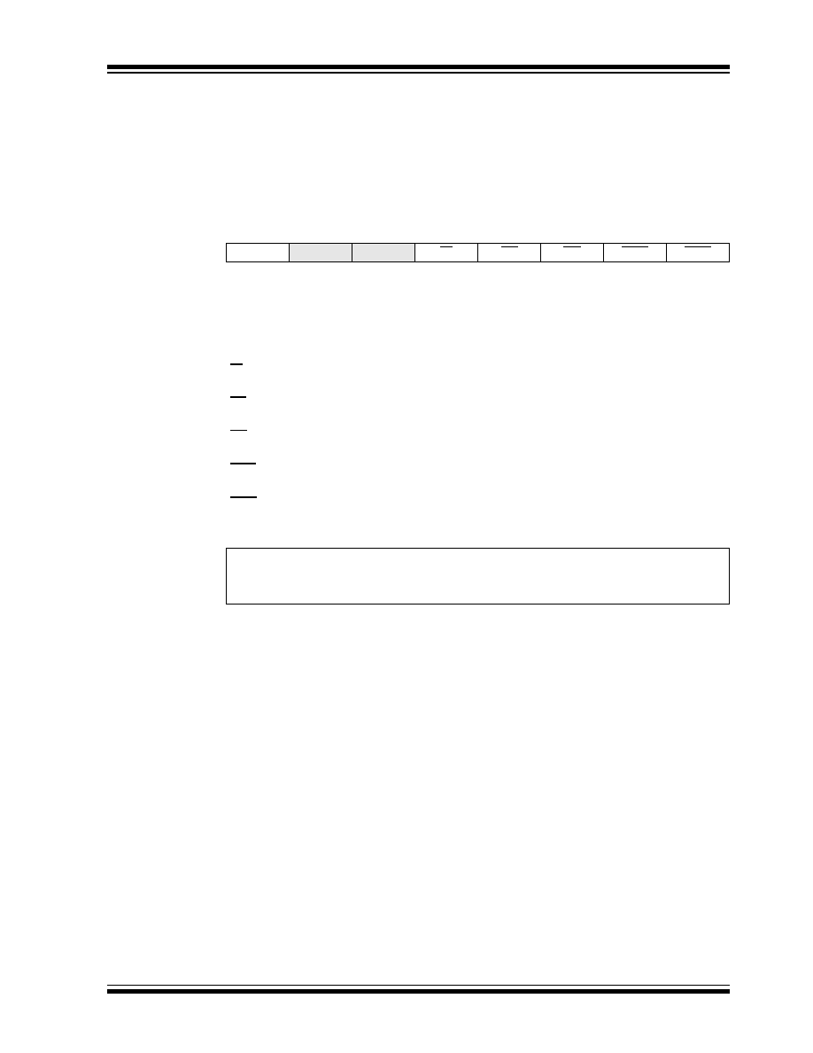
2002 Microchip Technology Inc
Preliminary
DS41159B-page 91
PIC18FXX8
8.5
RCON Register
The Reset Control (RCON) register contains the IPEN
bit, which is used to enable prioritized interrupts. The
functions of the other bits in this register are discussed
in more detail in Section 4.14.
REGISTER 8-13:
RCON REGISTER
R/W-0
U-0
U-0
R/W-1
R-1
R-1
R/W-0
R/W-0
IPEN
--
--
RI
TO
PD
POR
BOR
bit 7
bit 0
bit 7
IPEN: Interrupt Priority Enable bit
1
= Enable priority levels on interrupts
0
= Disable priority levels on interrupts (16CXXX Compatibility mode)
bit 6-5
Unimplemented: Read as '0'
bit 4
RI:
RESET
Instruction Flag bit
For details of bit operation, see Register 4-3
bit 3
TO: Watchdog Time-out Flag bit
For details of bit operation, see Register 4-3
bit 2
PD: Power-down Detection Flag bit
For details of bit operation, see Register 4-3
bit 1
POR: Power-on Reset Status bit
For details of bit operation, see Register 4-3
bit 0
BOR: Brown-out Reset Status bit
For details of bit operation, see Register 4-3
Legend:
R = Readable bit
W = Writable bit
U = Unimplemented bit, read as `0'
- n = Value at POR
'1' = Bit is set
'0' = Bit is cleared
x = Bit is unknown

PIC18FXX8
DS41159B-page 92
Preliminary
2002 Microchip Technology Inc.
8.6
INT Interrupts
External interrupts on the RB0/INT0, RB1/INT1 and
RB2/INT2 pins are edge triggered: either rising, if the
corresponding INTEDGx bit is set in the INTCON2 reg-
ister, or falling, if the INTEDGx bit is clear. When a valid
edge appears on the RBx/INTx pin, the corresponding
flag bit INTxIF is set. This interrupt can be disabled by
clearing the corresponding enable bit INTxIE. Flag bit
INTxIF must be cleared in software in the Interrupt Ser-
vice Routine before re-enabling the interrupt. All exter-
nal interrupts (INT0, INT1 and INT2) can wake-up the
processor from SLEEP, if bit INTxIE was set prior to
going into SLEEP. If the global interrupt enable bit GIE
is set, the processor will branch to the interrupt vector
following wake-up.
Interrupt priority for INT1 and INT2 is determined by the
value contained in the interrupt priority bits INT1IP
(INTCON3<6>) and INT2IP (INTCON3<7>). There is
no priority bit associated with INT0; it is always a high
priority interrupt source.
8.7
TMR0 Interrupt
In 8-bit mode (which is the default), an overflow (FFh
00h) in the TMR0 register will set flag bit TMR0IF. In 16-
bit mode, an overflow (FFFFh
0000h) in the
TMR0H:TMR0L registers will set flag bit TMR0IF. The
interrupt can be enabled/disabled by setting/clearing
enable bit TMR0IE (INTCON register). Interrupt priority
for Timer0 is determined by the value contained in the
interrupt priority bit TMR0IP (INTCON2 register). See
Section 11.0 for further details on the Timer0 module.
8.8
PORTB Interrupt-on-Change
An input change on PORTB<7:4> sets flag bit RBIF
(INTCON register). The interrupt can be enabled/
disabled by setting/clearing enable bit RBIE (INTCON
register). Interrupt priority for PORTB interrupt-on-
change is determined by the value contained in the
interrupt priority bit RBIP (INTCON2 register).
8.9
Context Saving During Interrupts
During an interrupt, the return PC value is saved on the
stack. Additionally, the WREG, STATUS and BSR regis-
ters are saved on the fast return stack. If a fast return
from interrupt is not used (see Section 4.3), the user
may need to save the WREG, STATUS and BSR regis-
ters in software. Depending on the user's application,
other registers may also need to be saved. Example 8-1
saves and restores the WREG, STATUS and BSR
registers during an Interrupt Service Routine.
EXAMPLE 8-1:
SAVING STATUS, WREG AND BSR REGISTERS IN RAM
MOVWF
W_TEMP
; W_TEMP is in Low Access bank
MOVFF
STATUS, STATUS_TEMP
; STATUS_TEMP located anywhere
MOVFF
BSR, BSR_TEMP
; BSR located anywhere
;
; USER ISR CODE
;
MOVFF
BSR_TEMP, BSR
; Restore BSR
MOVF
W_TEMP, W
; Restore WREG
MOVFF
STATUS_TEMP, STATUS
; Restore STATUS
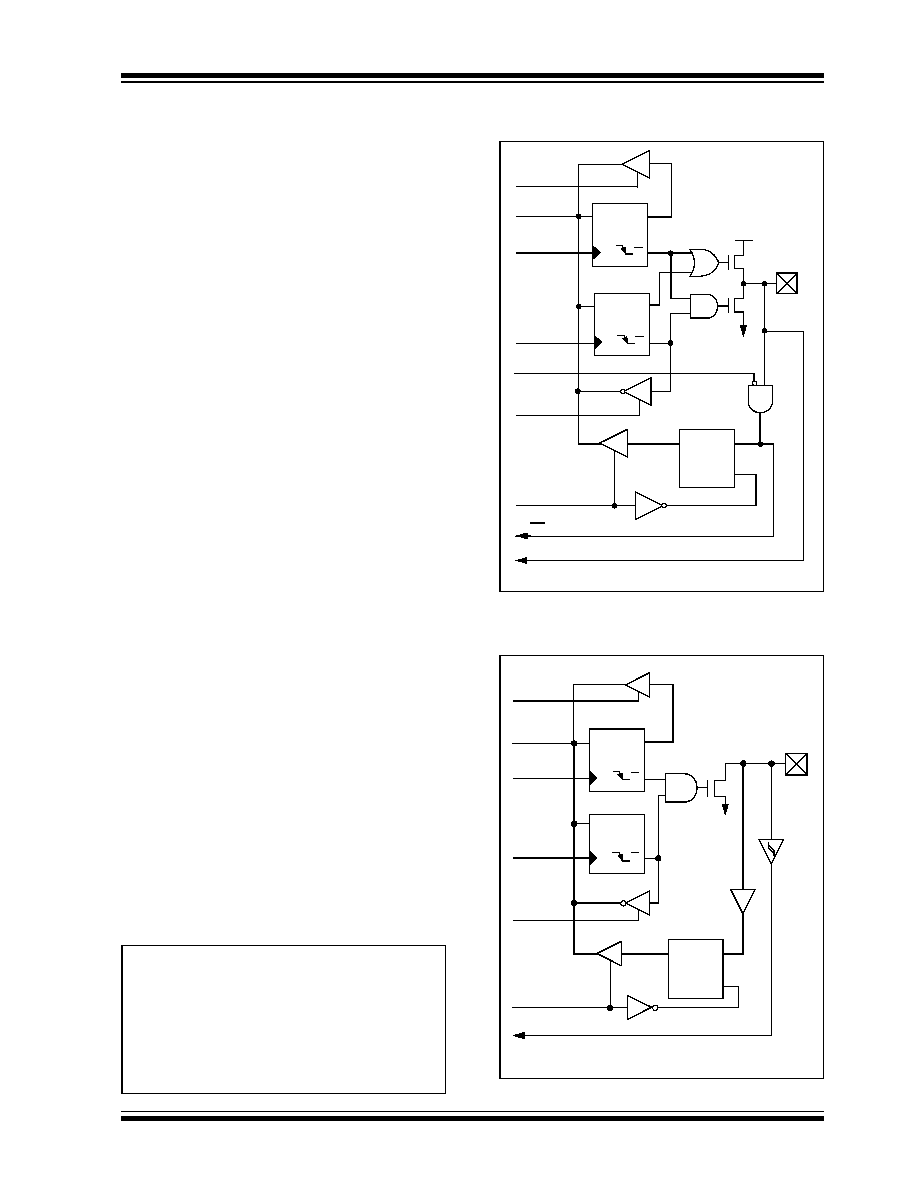
2002 Microchip Technology Inc.
Preliminary
DS41159B-page 93
PIC18FXX8
9.0
I/O PORTS
Depending on the device selected, there are up to five
general purpose I/O ports available on PIC18FXX8
devices. Some pins of the I/O ports are multiplexed
with an alternate function from the peripheral features
on the device. In general, when a peripheral is enabled,
that pin may not be used as a general purpose I/O pin.
Each port has three registers for its operation:
� TRIS register (Data Direction register)
� PORT register (reads the levels on the pins of the
device)
� LAT register (output latch).
The data latch (LAT register) is useful for
read-modify-write operations on the value that the I/O
pins are driving.
9.1
PORTA, TRISA and LATA
Registers
PORTA is a 7-bit wide, bi-directional port. The corre-
sponding Data Direction register is TRISA. Setting a
TRISA bit (= `
1
') will make the corresponding PORTA
pin an input (i.e., put the corresponding output driver in
a High-Impedance mode). Clearing a TRISA bit (= `
0
')
will make the corresponding PORTA pin an output (i.e.,
put the contents of the output latch on the selected pin).
On a Power-on Reset, these pins are configured as
inputs and read as '
0
'.
Reading the PORTA register reads the status of the
pins, whereas writing to it will write to the port latch.
Read-modify-write operations on the LATA register,
reads and writes the latched output value for PORTA.
The RA4 pin is multiplexed with the Timer0 module
clock input to become the RA4/T0CKI pin. The
RA4/T0CKI pin is a Schmitt Trigger input and an open
drain output. All other RA port pins have TTL input
levels and full CMOS output drivers.
The other PORTA pins are multiplexed with analog
inputs and the analog V
REF
+ and V
REF
- inputs. The
operation of each pin is selected by clearing/setting the
control bits in the ADCON1 register (A/D Control
Register 1). On a Power-on Reset, these pins are
configured as analog inputs and read as '
0
'.
The TRISA register controls the direction of the RA
pins, even when they are being used as analog inputs.
The user must ensure the bits in the TRISA register are
maintained set, when using them as analog inputs.
EXAMPLE 9-1:
INITIALIZING PORTA
FIGURE 9-1:
RA3:RA0 AND RA5 PINS
BLOCK DIAGRAM
FIGURE 9-2:
RA4/T0CKI PIN BLOCK
DIAGRAM
CLRF
PORTA
; Initialize PORTA by
; clearing output data latches
CLRF
LATA
; Alternate method to clear
; output data latches
MOVLW
07h
; Configure A/D
MOVWF
ADCON1 ; for digital inputs
MOVLW
0xCF
; Value used to initialize
; data direction
MOVWF
TRISA
; Set RA3:RA0 as inputs,
; RA5:RA4 as outputs
Data Bus
P
N
WR LATA
WR TRISA
Data Latch
TRIS Latch
RD TRISA
RD PORTA
V
SS
V
DD
I/O pin
(1)
Note 1:
I/O pins have diode protection to V
DD
and V
SS
.
Analog
Input Mode
TTL
Input
Buffer
To A/D Converter and LVD Modules
RD LATA
or
WR PORTA
SS Input (RA5 only)
Q
D
Q
CK
Q
D
Q
CK
Q
D
EN
Data Bus
WR TRISA
RD PORTA
Data Latch
TRIS Latch
RD TRISA
Schmitt
Trigger
Input
Buffer
N
V
SS
I/O pin
(1)
TMR0 Clock Input
Note 1: I/O pin has diode protection to V
SS
only.
Q
D
Q
CK
Q
D
Q
CK
Q
D
EN
RD LATA
WR LATA or
WR PORTA
TTL
Input
Buffer
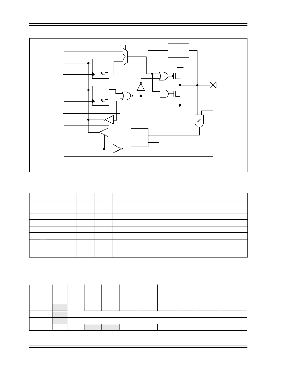
PIC18FXX8
DS41159B-page 94
Preliminary
2002 Microchip Technology Inc.
FIGURE 9-3:
RA6/OSC2/CLKOUT PIN BLOCK DIAGRAM
TABLE 9-1:
PORTA FUNCTIONS
TABLE 9-2:
SUMMARY OF REGISTERS ASSOCIATED WITH PORTA
Data Bus
P
N
WR PORTA
WR TRISA
Data Latch
TRIS Latch
RD TRISA
RD PORTA
V
SS
V
DD
Oscillator
Circuit
From OSC1
1
0
(F
OSC
=
101
,
111
)
Data Latch
CLKO (F
OSC
/4)
RA6/OSC2/
CLKO pin
(2)
(F
OSC
=
100
,
Schmitt
Trigger
Input Buffer
(F
OSC
=
110
,
100
)
Q
D
Q
CK
Q
D
Q
CK
Q
D
EN
101
,
110
,
111
)
Note
1: CLKO is 1/4 of F
OSC
.
2: I/O pin has diode protection to V
DD
and V
SS
.
Name
Bit#
Buffer Function
RA0/AN0/CV
REF
bit0
TTL
Input/output, analog input, or analog comparator voltage reference
output.
RA1/AN1
bit1
TTL
Input/output or analog input.
RA2/AN2/V
REF
-
bit2
TTL
Input/output, analog input or V
REF
-.
RA3/AN3/V
REF
+
bit3
TTL
Input/output, analog input or V
REF
+.
RA4/T0CKI
bit4
ST/OD
Input/output, external clock input for Timer0, output is open drain type.
RA5/SS/AN4/LVDIN
bit5
TTL
Input/output, slave select input for synchronous serial port, analog input,
or low voltage detect input.
RA6/OSC2/CLKO
bit6
TTL
Input/output or oscillator clock output.
Legend: TTL = TTL input, ST = Schmitt Trigger input, OD = Open Drain
Name
Bit 7
Bit 6
Bit 5
Bit 4
Bit 3
Bit 2
Bit 1
Bit 0
Value on
POR, BOR
Value on
all other
RESETS
PORTA
--
RA6
RA5
RA4
RA3
RA2
RA1
RA0
-00x 0000
-uuu uuuu
LATA
--
Latch A Data Output Register
-xxx xxxx
-uuu uuuu
TRISA
--
PORTA Data Direction Register
-111 1111
-111 1111
ADCON1
ADFM ADCS2
--
--
PCFG3
PCFG2
PCFG1
PCFG0
00-- 0000
uu-- uuuu
Legend:
x
= unknown,
u
= unchanged, - = unimplemented locations read as '
0
'. Shaded cells are not used by PORTA.
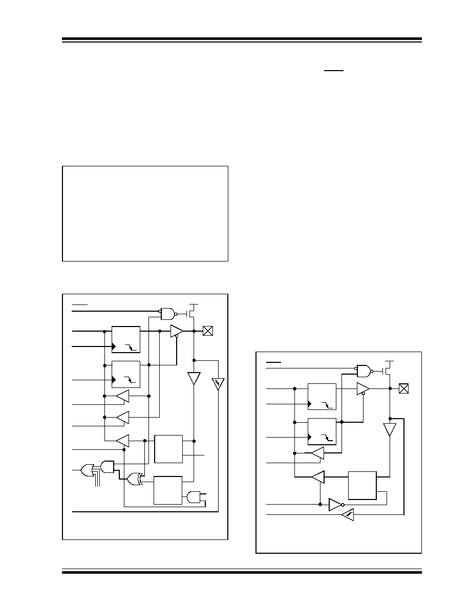
2002 Microchip Technology Inc.
Preliminary
DS41159B-page 95
PIC18FXX8
9.2
PORTB, TRISB and LATB Registers
PORTB is an 8-bit wide, bi-directional port. The corre-
sponding Data Direction register is TRISB. Setting a
TRISB bit (= `
1
') will make the corresponding PORTB
pin an input (i.e., put the corresponding output driver in
a High-Impedance mode). Clearing a TRISB bit (= `
0
')
will make the corresponding PORTB pin an output ( i.e.,
put the contents of the output latch on the selected pin).
Read-modify-write operations on the LATB register,
read and write the latched output value for PORTB.
EXAMPLE 9-2:
INITIALIZING PORTB
FIGURE 9-4:
RB7:RB4 PINS BLOCK
DIAGRAM
Each of the PORTB pins has a weak internal pull-up. A
single control bit can turn on all the pull-ups. This is per-
formed by clearing bit RBPU (INTCON2 register). The
weak pull-up is automatically turned off when the port
pin is configured as an output. The pull-ups are
disabled on a Power-on Reset.
Four of the PORTB pins (RB7:RB4) have an
interrupt-on-change feature. Only pins configured as
inputs can cause this interrupt to occur (i.e., any
RB7:RB4 pin configured as an output is excluded from
the interrupt-on-change comparison). The input pins (of
RB7:RB4) are compared with the old value latched on
the last read of PORTB. The "mismatch" outputs of
RB7:RB4 are ORed together to generate the RB Port
Change Interrupt with flag bit RBIF (INTCON register).
This interrupt can wake the device from SLEEP. The
user, in the Interrupt Service Routine, can clear the
interrupt in the following manner:
a)
Any read or write of PORTB (except with the
MOVFF
instruction). This will end the mismatch
condition.
b)
Clear flag bit RBIF.
A mismatch condition will continue to set flag bit RBIF.
Reading PORTB will end the mismatch condition and
allow flag bit RBIF to be cleared.
The interrupt-on-change feature is recommended for
wake-up on key depression operation and operations
where PORTB is only used for the interrupt-on-change
feature. Polling of PORTB is not recommended while
using the interrupt-on-change feature.
FIGURE 9-5:
RB1:RB0 PINS BLOCK
DIAGRAM
CLRF
PORTB
; Initialize PORTB by
; clearing output
; data latches
CLRF
LATB
; Alternate method
; to clear output
; data latches
MOVLW
0CFh
; Value used to
; initialize data
; direction
MOVWF
TRISB
; Set RB3:RB0 as inputs
; RB5:RB4 as outputs
; RB7:RB6 as inputs
Data Latch
From other
RBPU
(2)
P
V
DD
I/O pin
(1)
Q
D
CK
Q
D
CK
Q
D
EN
Q
D
EN
Data Bus
WR LATB
WR TRISB
Set RBIF
TRIS Latch
RD TRISB
RD PORTB
RB7:RB4 pins
Weak
Pull-up
Latch
TTL
Input
Buffer
ST
Buffer
RBx/INTx
Q3
Q1
RD LATB
or
WR PORTB
Note 1: I/O pins have diode protection to V
DD
and V
SS
.
2: To enable weak pull-ups, set the appropriate TRIS
bit(s) and clear the RBPU bit (INTCON2 register).
Data Latch
RBPU
(2)
P
V
DD
Q
D
CK
Q
D
CK
Q
D
EN
Data Bus
WR Port
WR TRIS
RD TRIS
RD Port
Weak
Pull-up
RBx/INTx
I/O pin
(1)
TTL
Input
Buffer
Schmitt Trigger
Buffer
TRIS Latch
Note 1: I/O pins have diode protection to V
DD
and V
SS
.
2: To enable weak pull-ups, set the appropriate TRIS
bit(s) and clear the RBPU bit (INTCON2 register).
PIC18FXX8
DS41159B-page 96
Preliminary
2002 Microchip Technology Inc.
FIGURE 9-6:
RB2/CANTX BLOCK DIAGRAM
FIGURE 9-7:
BLOCK DIAGRAM OF RB3/CANRX PIN
Data Latch
TRIS Latch
RD TRISB
P
V
SS
Q
D
Q
CK
Q
D
Q
CK
Q
D
EN
N
V
DD
0
1
RD PORTB
WR TRISB
Data Bus
RB2 pin
(1)
CANTX
ENDRHI
OPMODE2:OPMODE0 =
000
Schmitt
Trigger
RD LATB
WR PORTB or
WR LATB
Note 1: I/O pin has diode protection to V
DD
and V
SS
.
Data Latch
RBPU
(2)
P
V
DD
Q
D
CK
Q
D
CK
Q
D
EN
Data Bus
WR LATB or PORTB
WR TRISB
RD TRISB
RD PORTB
Weak
Pull-up
RB3 or CANRX
I/O
pin
(1)
TTL
Input
Buffer
Schmitt
Trigger
Buffer
TRIS Latch
RD LATB
CANCON<7:5>
.
Note 1: I/O pins have diode protection to V
DD
and V
SS
.
2: To enable weak pull-ups, set the appropriate TRIS bit(s) and clear the RBPU bit (INTCON2<7>).
2002 Microchip Technology Inc.
Preliminary
DS41159B-page 97
PIC18FXX8
TABLE 9-3:
PORTB FUNCTIONS
TABLE 9-4:
SUMMARY OF REGISTERS ASSOCIATED WITH PORTB
Name
Bit#
Buffer Function
RB0/INT0
bit0
TTL/ST
(1)
Input/output pin or external interrupt 0 input.
Internal software programmable weak pull-up.
RB1/INT1
bit1
TTL/ST
(1)
Input/output pin or external interrupt 1 input.
Internal software programmable weak pull-up.
RB2/INT2/
CANTX
bit2
TTL/ST
(1)
Input/output pin, external interrupt 2 input or CAN bus transmit pin.
Internal software programmable weak pull-up.
RB3/CANRX
bit3
TTL
Input/output pin or CAN bus receive pin.
Internal software programmable weak pull-up.
RB4
bit4
TTL
Input/output pin (with interrupt-on-change).
Internal software programmable weak pull-up.
RB5/PGM
bit5
TTL
Input/output pin (with interrupt-on-change). Internal software programmable
weak pull-up. Low voltage serial programming enable.
RB6/PGC
bit6
TTL/ST
(2)
Input/output pin (with interrupt-on-change). Internal software programmable
weak pull-up. Serial programming clock.
RB7/PGD
bit7
TTL/ST
(2)
Input/output pin (with interrupt-on-change). Internal software programmable
weak pull-up. Serial programming data.
Legend: TTL = TTL input, ST = Schmitt Trigger input
Note 1: This buffer is a Schmitt Trigger input when configured as the external interrupt.
2: This buffer is a Schmitt Trigger input when used in Serial Programming mode.
Name
Bit 7
Bit 6
Bit 5
Bit 4
Bit 3
Bit 2
Bit 1
Bit 0
Value on
POR, BOR
Value on
all other
RESETS
PORTB
RB7
RB6
RB5
RB4
RB3
RB2
RB1
RB0
xxxx xxxx
uuuu uuuu
LATB
LATB Data Output Register
xxxx xxxx
uuuu uuuu
TRISB
PORTB Data Direction Register
1111 1111
1111 1111
INTCON
GIE/GIEH PEIE/GIEL
TMR0IE
INT0IE
RBIE
TMR0IF
INT0IF
RBIF
0000 000x
0000 000u
INTCON2
RBPU
INTEDG0 INTEDG1
INTEDG2
--
TMR0IP
--
RBIP
1111 -1-1
1111 -1-1
INTCON3
INT2IP
INT1IP
--
INT2IE
INT1IE
--
INT2IF
INT1IF
11-0 0-00
11-0 0-00
Legend:
x
= unknown,
u
= unchanged. Shaded cells are not used by PORTB.
PIC18FXX8
DS41159B-page 98
Preliminary
2002 Microchip Technology Inc.
9.3
PORTC, TRISC and LATC Registers
PORTC is an 8-bit wide, bi-directional port. The corre-
sponding Data Direction register is TRISC. Setting a
TRISC bit (= `
1
') will make the corresponding PORTC
pin an input (i.e., put the corresponding output driver in
a High-Impedance mode). Clearing a TRISC bit (= `
0
')
will make the corresponding PORTC pin an output (i.e.,
put the contents of the output latch on the selected pin).
Read-modify-write operations on the LATC register,
read and write the latched output value for PORTC.
PORTC is multiplexed with several peripheral functions
(Table 9-5). PORTC pins have Schmitt Trigger input
buffers.
When enabling peripheral functions, care should be
taken in defining TRIS bits for each PORTC pin. Some
peripherals override the TRIS bit to make a pin an output,
while other peripherals override the TRIS bit to make a
pin an input. The user should refer to the corresponding
peripheral section for the correct TRIS bit settings.
The pin override value is not loaded into the TRIS reg-
ister. This allows read-modify-write of the TRIS register,
without concern due to peripheral overrides.
EXAMPLE 9-3:
INITIALIZING PORTC
FIGURE 9-8:
PORTC BLOCK DIAGRAM (PERIPHERAL OUTPUT OVERRIDE)
CLRF
PORTC
; Initialize PORTC by
; clearing output
; data latches
CLRF
LATC
; Alternate method
; to clear output
; data latches
MOVLW
0CFh
; Value used to
; initialize data
; direction
MOVWF
TRISC
; Set RC3:RC0 as inputs
; RC5:RC4 as outputs
; RC7:RC6 as inputs
Peripheral Out Select
Data Bus
WR LATC
WR TRISC
Data Latch
TRIS Latch
RD TRISC
Q
D
Q
CK
Q
D
EN
Peripheral Data Out
0
1
Q
D
Q
CK
P
N
V
DD
V
SS
RD PORTC
Peripheral Data In
I/O pin
(1)
or
WR PORTC
RD LATC
Schmitt
Trigger
Note
1: I/O pins have diode protection to V
DD
and V
SS
.
TRIS
Override
Peripheral Enable
TRIS OVERRIDE
Pin
Override
Peripheral
RC0
Yes
Timer1 OSC for
Timer1/Timer3
RC1
Yes
Timer1 OSC for
Timer1/Timer3
RC2
No
--
RC3
Yes
SPI/I
2
C Master
Clock
RC4
Yes
I
2
C Data Out
RC5
Yes
SPI Data Out
RC6
Yes
USART Async
Xmit, Sync Clock
RC7
Yes
USART Sync
Data Out

2002 Microchip Technology Inc.
Preliminary
DS41159B-page 99
PIC18FXX8
TABLE 9-5:
PORTC FUNCTIONS
TABLE 9-6:
SUMMARY OF REGISTERS ASSOCIATED WITH PORTC
Name
Bit#
Buffer Type
Function
RC0/T1OSO/T1CKI
bit0
ST
Input/output port pin, Timer1 oscillator output or Timer1/Timer3 clock
input.
RC1/T1OSI
bit1
ST
Input/output port pin or Timer1 oscillator input.
RC2/CCP1
bit2
ST
Input/output port pin or Capture1 input/Compare1 output/PWM1 output.
RC3/SCK/SCL
bit3
ST
Input/output port pin or Synchronous Serial clock for SPI/I
2
C.
RC4/SDI/SDA
bit4
ST
Input/output port pin or SPI Data in (SPI mode) or Data I/O (I
2
C mode).
RC5/SDO
bit5
ST
Input/output port pin or Synchronous Serial Port data output.
RC6/TX/CK
bit6
ST
Input/output port pin, Addressable USART Asynchronous Transmit or
Addressable USART Synchronous Clock.
RC7/RX/DT
bit7
ST
Input/output port pin, Addressable USART Asynchronous Receive or
Addressable USART Synchronous Data.
Legend: ST = Schmitt Trigger input
Name
Bit 7
Bit 6
Bit 5
Bit 4
Bit 3
Bit 2
Bit 1
Bit 0
Value on
POR, BOR
Value on
all other
RESETS
PORTC
RC7
RC6
RC5
RC4
RC3
RC2
RC1
RC0
xxxx xxxx
uuuu uuuu
LATC
LATC Data Output Register
xxxx xxxx
uuuu uuuu
TRISC
PORTC Data Direction Register
1111 1111
1111 1111
Legend:
x
= unknown,
u
= unchanged
PIC18FXX8
DS41159B-page 100
Preliminary
2002 Microchip Technology Inc.
9.4
PORTD, TRISD and LATD
Registers
PORTD is an 8-bit wide, bi-directional port. The corre-
sponding Data Direction register for the port is TRISD.
Setting a TRISD bit (= `
1
') will make the corresponding
PORTD pin an input (i.e., put the corresponding output
driver in a High-Impedance mode). Clearing a TRISD
bit (= `
0
') will make the corresponding PORTD pin an
output (i.e., put the contents of the output latch on the
selected pin).
Read-modify-write operations on the LATD register
reads and writes the latched output value for PORTD.
PORTD is uses Schmitt Trigger input buffers. Each pin
is individually configurable as an input or output.
PORTD can be configured as an 8-bit wide micro-
processor port (Parallel Slave Port, or PSP) by setting
the control bit PSPMODE (TRISE<4>). In this mode,
the input buffers are TTL. See Section 10.0 for
additional information on the Parallel Slave Port.
PORTD is also multiplexed with the analog comparator
module and the ECCP module.
EXAMPLE 9-4:
INITIALIZING PORTD
FIGURE 9-9:
PORTD BLOCK DIAGRAM IN I/O PORT MODE
Note:
This port is only available on the
PIC18F448 and PIC18F458.
CLRF
PORTD
; Initialize PORTD by
; clearing output
; data latches
CLRF
LATD
; Alternate method
; to clear output
; data latches
MOVLW
07h
; comparator off
MOVWF
CMCON
MOVLW
0CFh
; Value used to
; initialize data
; direction
MOVWF
TRISD
; Set RD3:RD0 as inputs
; RD5:RD4 as outputs
; RD7:RD6 as inputs
PORT/PSP Select
Data Bus
WR LATD
WR TRISD
Data Latch
TRIS Latch
RD TRISD
Q
D
Q
CK
Q
D
EN
Q
D
Q
CK
P
N
V
DD
Vss
RD PORTD
RD0 pin
(1)
or
PORTD
RD LATD
Schmitt
Trigger
Note
1:
I/O pins have diode protection to V
DD
and V
SS
.
PSP Data Out
PSP Write
PSP Read
C1IN+
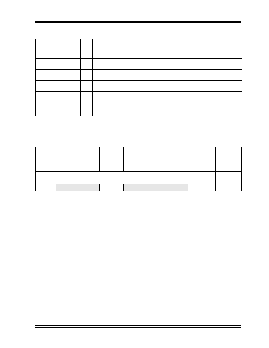
2002 Microchip Technology Inc.
Preliminary
DS41159B-page 101
PIC18FXX8
TABLE 9-7:
PORTD FUNCTIONS
TABLE 9-8:
SUMMARY OF REGISTERS ASSOCIATED WITH PORTD
Name
Bit#
Buffer Type
Function
RD0/PSP0/C1IN+ bit0
ST/TTL
(1)
Input/output port pin, parallel slave port bit0 or C1IN+ Comparator
input.
RD1/PSP1/C1IN-
bit1 ST/TTL
(1)
Input/output port pin, parallel slave port bit1 or C1IN- Comparator
input.
RD2/PSP2/C2IN+
bit2
ST/TTL
(1)
Input/output port pin, parallel slave port bit2 or C2IN+ Comparator
input.
RD3/PSP3/C2IN-
bit3
ST/TTL
(1)
Input/output port pin, parallel slave port bit3 or C2IN- Comparator
input.
RD4/PSP4/ECCP1/P1A
bit4
ST/TTL
(1)
Input/output port pin, parallel slave port bit4 or ECCP1/P1A pin.
RD5/PSP5/P1B
bit5
ST/TTL
(1)
Input/output port pin, parallel slave port bit5 or ECCP1/P1B pin.
RD6/PSP6/P1C
bit6
ST/TTL
(1)
Input/output port pin, parallel slave port bit6 or ECCP1/P1C pin.
RD7/PSP7/P1D
bit7
ST/TTL
(1)
Input/output port pin, parallel slave port bit7 or ECCP1/P1D pin.
Legend: ST = Schmitt Trigger input, TTL = TTL input
Note 1: Input buffers are Schmitt Triggers when in I/O mode and TTL buffers when in Parallel Slave Port mode.
Name
Bit 7
Bit 6
Bit 5
Bit 4
Bit 3
Bit 2
Bit 1
Bit 0
Value on
POR, BOR
Value on
all other
RESETS
PORTD
RD7
RD6
RD5
RD4
RD3
RD2
RD1
RD0
xxxx xxxx
uuuu uuuu
LATD
LATD Data Output Register
xxxx xxxx
uuuu uuuu
TRISD
PORTD Data Direction Register
1111 1111
1111 1111
TRISE
IBF
OBF
IBOV
PSPMODE
--
TRISE2
TRISE1 TRISE0
0000 -111
0000 -111
Legend:
x
= unknown,
u
= unchanged,
-
= unimplemented, read as '
0
'. Shaded cells are not used by PORTD.
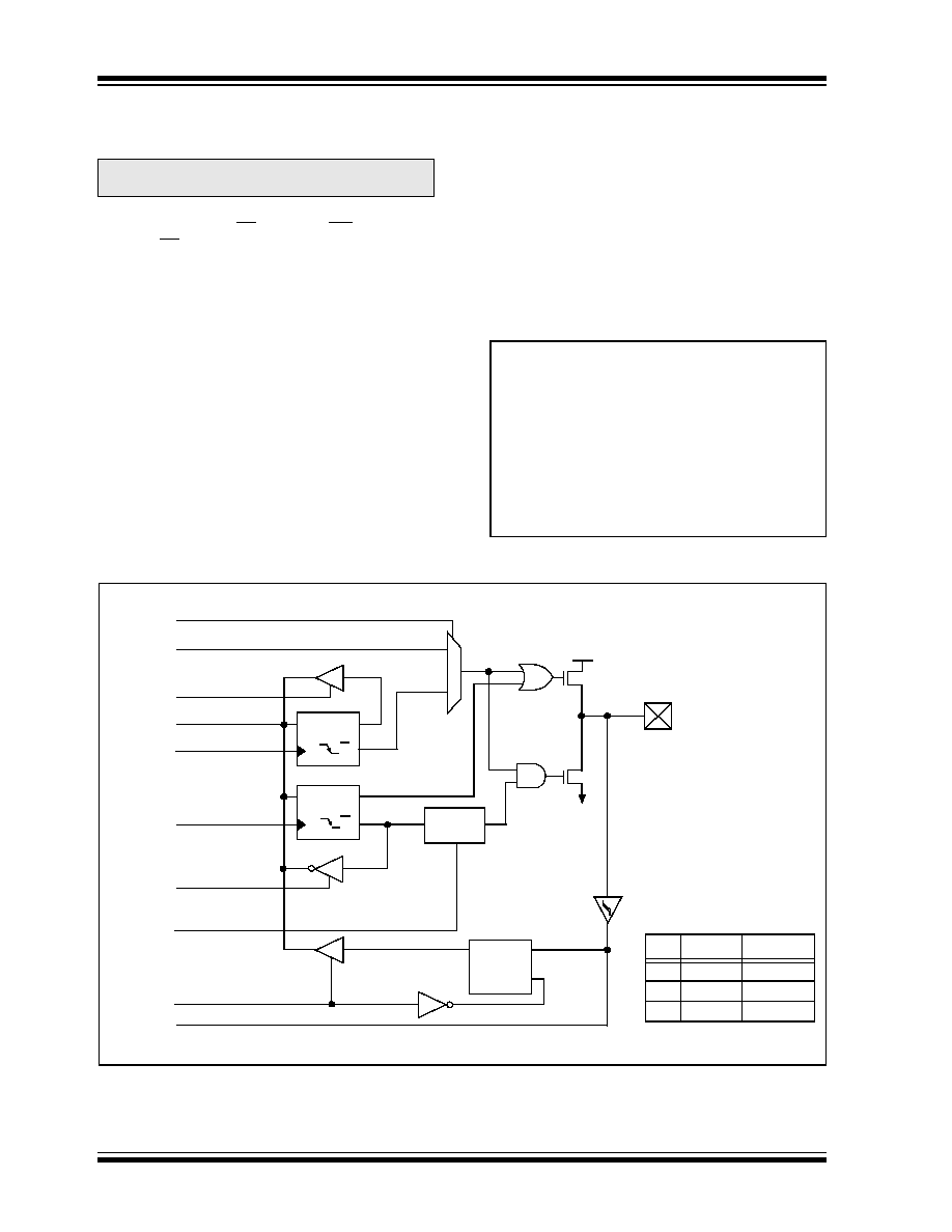
PIC18FXX8
DS41159B-page 102
Preliminary
2002 Microchip Technology Inc.
9.5
PORTE, TRISE and LATE
Registers
PORTE is a 3-bit wide, bi-directional port. PORTE has
three pins (RE0/AN5/RD, RE1/AN6/WR/C1OUT and
RE2/AN7/CS/C2OUT), which are individually config-
urable as inputs or outputs. These pins have Schmitt
Trigger input buffers.
Read-modify-write operations on the LATE register,
reads and writes the latched output value for PORTE.
The corresponding Data Direction register for the port
is TRISE. Setting a TRISE bit (= `
1
') will make the cor-
responding PORTE pin an input (i.e., put the corre-
sponding output driver in a High-Impedance mode).
Clearing a TRISE bit (= `
0
') will make the corresponding
PORTE pin an output (i.e., put the contents of the
output latch on the selected pin).
The TRISE register also controls the operation of the
Parallel Slave Port, through the control bits in the upper
half of the register. These are shown in Register 9-1.
When the Parallel Slave Port is active, the PORTE pins
function as its control inputs. For additional details,
refer to Section 10.0.
PORTE pins are also multiplexed with inputs for the
A/D converter and outputs for the analog comparators.
When selected as an analog input, these pins will read
as '
0
's. Direction bits TRISE<2:0> control the direction
of the RE pins, even when they are being used as ana-
log inputs. The user must make sure to keep the pins
configured as inputs when using them as analog
inputs.
EXAMPLE 9-5:
INITIALIZING PORTE
FIGURE 9-10:
PORTE BLOCK DIAGRAM
Note:
This port is only available on the
PIC18F448 and PIC18F458.
CLRF
PORTE
; Initialize PORTE by
; clearing output
; data latches
CLRF
LATE
; Alternate method
; to clear output
; data latches
MOVLW
03h
; Value used to
; initialize data
; direction
MOVWF
TRISE
; Set RE1:RE0 as inputs
; RE2 as an output
; (RE4=0 - PSPMODE Off)
Peripheral Out Select
Data Bus
WR LATE
WR TRISE
Data
Latch
TRIS Latch
RD TRISE
Q
D
Q
CK
Q
D
EN
Peripheral Data Out
0
1
Q
D
Q
CK
P
N
V
DD
V
SS
RD PORTE
Peripheral Data In
I/O pin
(1)
or
WR PORTE
RD LATE
Schmitt
Trigger
Note
1: I/O pins have diode protection to V
DD
and V
SS
.
TRIS OVERRIDE
Pin
Override Peripheral
RE0
Yes
PSP
RE1
Yes
PSP
RE2
Yes
PSP
TRIS
Override
Peripheral Enable
2002 Microchip Technology Inc.
Preliminary
DS41159B-page 103
PIC18FXX8
REGISTER 9-1:
TRISE REGISTER
TABLE 9-9:
PORTE FUNCTIONS
R-0
R-0
R/W-0
R/W-0
U-0
R/W-1
R/W-1
R/W-1
IBF
OBF
IBOV
PSPMODE
--
TRISE2
TRISE1
TRISE0
bit 7
bit 0
bit 7
IBF: Input Buffer Full Status bit
1
= A word has been received and waiting to be read by the CPU
0
= No word has been received
bit 6
OBF: Output Buffer Full Status bit
1
= The output buffer still holds a previously written word
0
= The output buffer has been read
bit 5
IBOV: Input Buffer Overflow Detect bit (in Microprocessor mode)
1
= A write occurred when a previously input word has not been read
(must be cleared in software)
0
= No overflow occurred
bit 4
PSPMODE: Parallel Slave Port Mode Select bit
1
= Parallel Slave Port mode
0
= General purpose I/O mode
bit 3
Unimplemented: Read as '0'
bit 2
TRISE2: RE2 Direction Control bit
1
= Input
0
= Output
bit 1
TRISE1: RE1 Direction Control bit
1
= Input
0
= Output
bit 0
TRISE0: RE0 Direction Control bit
1
= Input
0
= Output
Legend:
R = Readable bit
W = Writable bit
U = Unimplemented bit, read as `0'
- n = Value at POR
'1' = Bit is set
'0' = Bit is cleared
x = Bit is unknown
Name
Bit#
Buffer Type
Function
RE0/AN5/RD
bit0
ST/TTL
(1)
Input/output port pin, analog input or read control input in Parallel
Slave Port mode.
RE1/AN6/WR/C1OUT
bit1
ST/TTL
(1)
Input/output port pin, analog input, write control input in Parallel Slave
Port mode or Comparator 1 output.
RE2/AN7/CS/C2OUT
bit2
ST/TTL
(1)
Input/output port pin, analog input, chip select control input in Parallel
Slave Port mode or Comparator 2 output.
Legend: ST = Schmitt Trigger input, TTL = TTL input
Note 1: Input buffers are Schmitt Triggers when in I/O mode and TTL buffers when in Parallel Slave Port mode.

PIC18FXX8
DS41159B-page 104
Preliminary
2002 Microchip Technology Inc.
TABLE 9-10:
SUMMARY OF REGISTERS ASSOCIATED WITH PORTE
Name
Bit 7
Bit 6
Bit 5
Bit 4
Bit 3
Bit 2
Bit 1
Bit 0
Value on:
POR, BOR
Value on
all other
RESETS
TRISE
IBF
OBF
IBOV
PSPMODE
--
TRISE2
TRISE1
TRISE0
0000 -111
0000 -111
PORTE
--
--
--
--
--
Read PORTE pin/
Write PORTE Data Latch
---- -xxx
---- -uuu
LATE
--
--
--
--
--
Read PORTE Data Latch/
Write PORTE Data Latch
---- -xxx
---- -uuu
Legend:
x
= unknown,
u
= unchanged,
-
= unimplemented, read as '
0
'. Shaded cells are not used by PORTE.
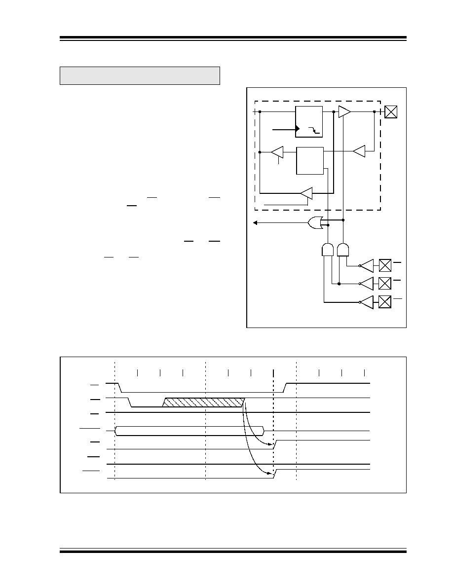
2002 Microchip Technology Inc.
Preliminary
DS41159B-page 105
PIC18FXX8
10.0
PARALLEL SLAVE PORT
In addition to its function as a general I/O port, PORTD
can also operate as an 8-bit wide Parallel Slave Port
(PSP), or microprocessor port. PSP operation is con-
trolled by the 4 upper bits of the TRISE register
(Register 9-1). Setting control bit PSPMODE
(TRISE<4>) enables PSP operation. In Slave mode,
the port is asynchronously readable and writable by the
external world.
The PSP can directly interface to an 8-bit microproces-
sor data bus. The external microprocessor can read or
write the PORTD latch as an 8-bit latch. Setting the
control bit PSPMODE enables the PORTE I/O pins to
become control inputs for the microprocessor port.
When set, port pin RE0 is the RD input, RE1 is the WR
input, and RE2 is the CS (chip select) input. For this
functionality, the corresponding data direction bits of
the TRISE register (TRISE<2:0>) must be configured
as inputs (set).
A write to the PSP occurs when both the CS and WR
lines are first detected low. A read from the PSP occurs
when both the CS and RD lines are first detected low.
The timing for the control signals in write and read
modes is shown in Figure 10-2 and Figure 10-3,
respectively.
FIGURE 10-1:
PORTD AND PORTE
BLOCK DIAGRAM
(PARALLEL SLAVE
PORT)
FIGURE 10-2:
PARALLEL SLAVE PORT WRITE WAVEFORMS
Note:
The Parallel Slave Port is only available on
PIC18F4X8 devices.
Data Bus
WR LATD
RDx pin
Q
D
CK
EN
Q
D
EN
RD PORTD
One bit of PORTD
Set Interrupt Flag
PSPIF (PIR1<7>)
Read
Chip Select
Write
RD
CS
WR
TTL
TTL
TTL
TTL
or
WR PORTD
RD LATD
Data Latch
Note:
I/O pins have diode protection to V
DD
and V
SS
.
PORTE pins
Q1
Q2
Q3
Q4
CS
Q1
Q2
Q3
Q4
Q1
Q2
Q3
Q4
WR
RD
IBF
OBF
PSPIF
PORTD
PIC18FXX8
DS41159B-page 106
Preliminary
2002 Microchip Technology Inc.
FIGURE 10-3:
PARALLEL SLAVE PORT READ WAVEFORMS
TABLE 10-1:
REGISTERS ASSOCIATED WITH PARALLEL SLAVE PORT
Q1
Q2
Q3
Q4
CS
Q1
Q2
Q3
Q4
Q1
Q2
Q3
Q4
WR
IBF
PSPIF
RD
OBF
PORTD
Name
Bit 7
Bit 6
Bit 5
Bit 4
Bit 3
Bit 2
Bit 1
Bit 0
Value on
POR, BOR
Value on
all other
RESETS
PORTD
Port Data Latch when written; Port pins when read
xxxx xxxx uuuu uuuu
LATD
LATD Data Output bits
xxxx xxxx uuuu uuuu
TRISD
PORTD Data Direction bits
1111 1111 1111 1111
PORTE
--
--
--
--
--
RE2
RE1
RE0
---- -000 ---- -000
LATE
LATE Data Output bits
---- -xxx ---- -uuu
TRISE
IBF
OBF
IBOV
PSPMODE
--
PORTE Data Direction bits
0000 -111 0000 -111
INTCON
GIE/GIEH PEIE/GIEL TMR0IE
INT0IE
RBIE
TMR0IF
INT0IF
RBIF
0000 000x 0000 000u
PIR1
PSPIF
ADIF
RCIF
TXIF
SSPIF
CCP1IF TMR2IF TMR1IF
0000 0000 0000 0000
PIE1
PSPIE
ADIE
RCIE
TXIE
SSPIE
CCP1IE TMR2IE TMR1IE
0000 0000 0000 0000
IPR1
PSPIP
ADIP
RCIP
TXIP
SSPIP
CCP1IP TMR2IP TMR1IP
0000 0000 0000 0000
Legend:
x
= unknown,
u
= unchanged, - = unimplemented, read as '0'. Shaded cells are not used by the Parallel Slave Port.
2002 Microchip Technology Inc.
Preliminary
DS41159B-page 107
PIC18FXX8
11.0
TIMER0 MODULE
The Timer0 module has the following features:
� Software selectable as an 8-bit or
16-bit timer/counter
� Readable and writable
� Dedicated 8-bit software programmable prescaler
� Clock source selectable to be external or internal
� Interrupt-on-overflow from FFh to 00h in 8-bit
mode, and FFFFh to 0000h in 16-bit mode
� Edge select for external clock
Register 11-1 shows the Timer0 Control register
(T0CON).
Figure 11-1 shows a simplified block diagram of the
Timer0 module in 8-bit mode and Figure 11-2 shows a
simplified block diagram of the Timer0 module in 16-bit
mode.
The T0CON register is a readable and writable register
that controls all the aspects of Timer0, including the
prescale selection.
REGISTER 11-1:
T0CON REGISTER
Note:
Timer0 is enabled on POR.
R/W-1
R/W-1
R/W-1
R/W-1
R/W-1
R/W-1
R/W-1
R/W-1
TMR0ON
T08BIT
T0CS
T0SE
PSA
T0PS2
T0PS1
T0PS0
bit 7
bit 0
bit 7
TMR0ON: Timer0 On/Off Control bit
1
= Enables Timer0
0
= Stops Timer0
bit 6
T08BIT: Timer0 8-bit/16-bit Control bit
1
= Timer0 is configured as an 8-bit timer/counter
0
= Timer0 is configured as a 16-bit timer/counter
bit 5
T0CS: Timer0 Clock Source Select bit
1
= Transition on T0CKI pin
0
= Internal instruction cycle clock (CLKO)
bit 4
T0SE: Timer0 Source Edge Select bit
1
= Increment on high-to-low transition on T0CKI pin
0
= Increment on low-to-high transition on T0CKI pin
bit 3
PSA: Timer0 Prescaler Assignment bit
1
= TImer0 prescaler is NOT assigned. Timer0 clock input bypasses prescaler.
0
= Timer0 prescaler is assigned. Timer0 clock input comes from prescaler output.
bit 2-0
T0PS2:T0PS0: Timer0 Prescaler Select bits
111
= 1:256 prescale value
110
= 1:128 prescale value
101
= 1:64 prescale value
100
= 1:32 prescale value
011
= 1:16 prescale value
010
= 1:8 prescale value
001
= 1:4 prescale value
000
= 1:2 prescale value
Legend:
R = Readable bit
W = Writable bit
U = Unimplemented bit, read as `0'
- n = Value at POR
'1' = Bit is set
'0' = Bit is cleared
x = Bit is unknown
PIC18FXX8
DS41159B-page 108
Preliminary
2002 Microchip Technology Inc.
FIGURE 11-1:
TIMER0 BLOCK DIAGRAM IN 8-BIT MODE
FIGURE 11-2:
TIMER0 BLOCK DIAGRAM IN 16-BIT MODE
Note 1: Upon RESET, Timer0 is enabled in 8-bit mode with clock input from T0CKI max. prescale.
2: I/O pins have diode protection to V
DD
and V
SS
.
RA4/T0CKI
T0SE
1
0
1
0
pin
(2)
T0CS
(1)
F
OSC
/4
Programmable
Prescaler
Sync with
Internal
Clocks
TMR0L
(2 T
CY
delay)
Data Bus
8
PSA
T0PS2, T0PS1, T0PS0
Set Interrupt
Flag bit TMR0IF
on Overflow
3
T0CKI pin
(2)
T0SE
1
0
1
0
T0CS
(1)
F
OSC
/4
Programmable
Prescaler
Sync with
Internal
Clocks
TMR0L
(2 T
CY
delay)
Data Bus<7:0>
8
PSA
T0PS2, T0PS1, T0PS0
Set Interrupt
Flag bit TMR0IF
on Overflow
3
TMR0
TMR0H
High Byte
8
8
8
Read TMR0L
Write TMR0L
Note 1: Upon RESET, Timer0 is enabled in 8-bit mode with clock input from T0CKI max. prescale.
2: I/O pins have diode protection to V
DD
and V
SS
.
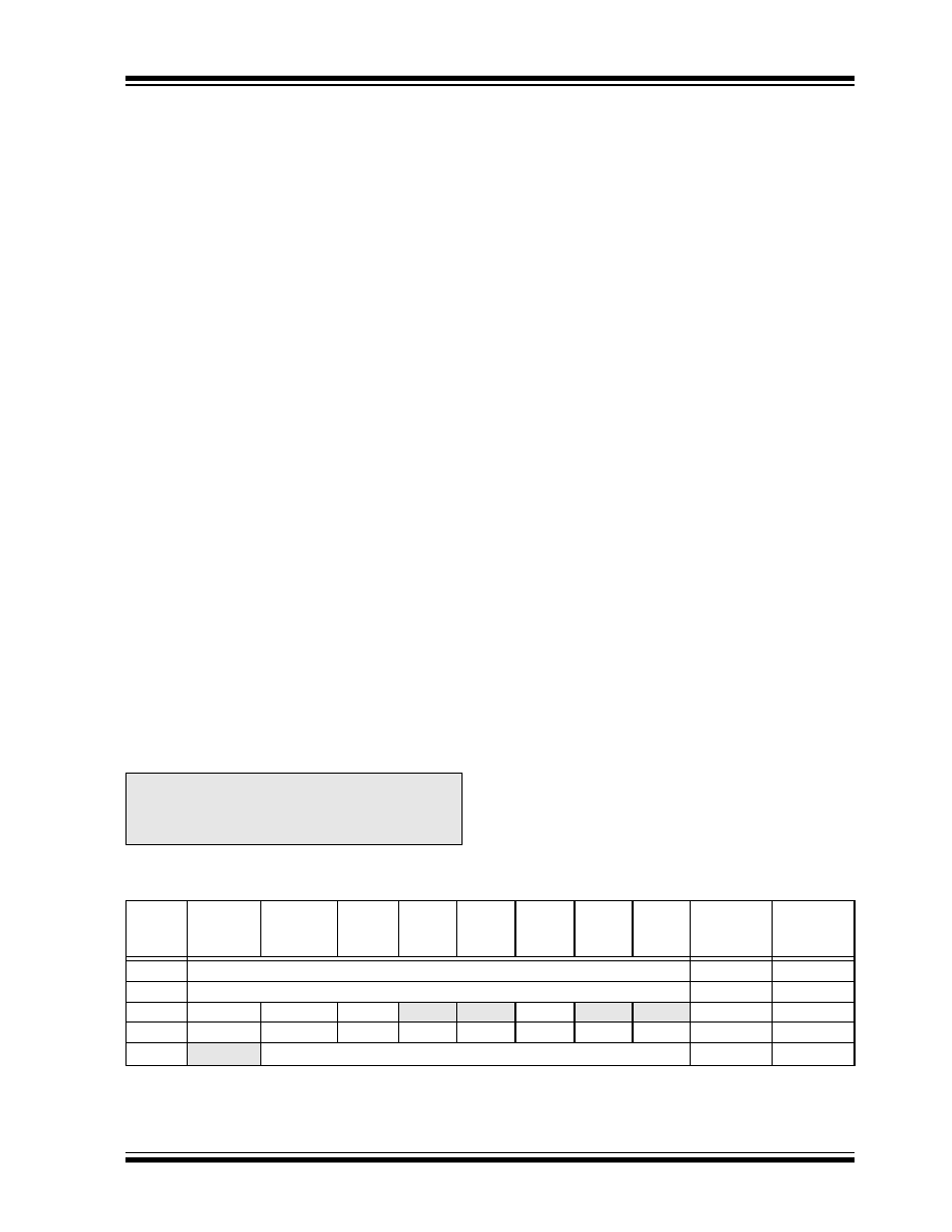
2002 Microchip Technology Inc.
Preliminary
DS41159B-page 109
PIC18FXX8
11.1
Timer0 Operation
Timer0 can operate as a timer or as a counter.
Timer mode is selected by clearing the T0CS bit. In
Timer mode, the Timer0 module will increment every
instruction cycle (without prescaler). If the TMR0L reg-
ister is written, the increment is inhibited for the follow-
ing two instruction cycles. The user can work around
this by writing an adjusted value to the TMR0L register.
Counter mode is selected by setting the T0CS bit. In
Counter mode, Timer0 will increment either on every
rising, or falling edge of pin RA4/T0CKI. The increment-
ing edge is determined by the Timer0 Source Edge
Select bit (T0SE). Clearing the T0SE bit selects the ris-
ing edge. Restrictions on the external clock input are
discussed below.
When an external clock input is used for Timer0, it must
meet certain requirements. The requirements ensure
the external clock can be synchronized with the internal
phase clock (T
OSC
). Also, there is a delay in the actual
incrementing of Timer0 after synchronization.
11.2
Prescaler
An 8-bit counter is available as a prescaler for the
Timer0 module. The prescaler is not readable or
writable.
The PSA and T0PS2:T0PS0 bits determine the
prescaler assignment and prescale ratio.
Clearing bit PSA will assign the prescaler to the Timer0
module. When the prescaler is assigned to the Timer0
module, prescale values of 1:2, 1:4, ..., 1:256 are
selectable.
When assigned to the Timer0 module, all instructions
writing to the TMR0 register (e.g.
CLRF TMR0, MOVWF
TMR0, BSF TMR0, x
.... etc.) will clear the prescaler
count.
11.2.1
SWITCHING PRESCALER
ASSIGNMENT
The prescaler assignment is fully under software con-
trol (i.e., it can be changed "on-the-fly" during program
execution).
11.3
Timer0 Interrupt
The TMR0 interrupt is generated when the TMR0 reg-
ister overflows from FFh to 00h in 8-bit mode, or FFFFh
to 0000h in 16-bit mode. This overflow sets the TMR0IF
bit. The interrupt can be masked by clearing the
TMR0IE bit. The TMR0IF bit must be cleared in soft-
ware by the Timer0 module Interrupt Service Routine
before re-enabling this interrupt. The TMR0 interrupt
cannot awaken the processor from SLEEP, since the
timer is shut-off during SLEEP.
11.4
16-bit Mode Timer Reads and
Writes
Timer0 can be set in 16-bit mode by clearing T0CON
T08BIT. Registers TMR0H and TMR0L are used to
access 16-bit timer value.
TMR0H is not the high byte of the timer/counter in
16-bit mode, but is actually a buffered version of the
high byte of Timer0 (refer to Figure 11-1). The high byte
of the Timer0 counter/timer is not directly readable nor
writable. TMR0H is updated with the contents of the
high byte of Timer0 during a read of TMR0L. This pro-
vides the ability to read all 16 bits of Timer0 without
having to verify that the read of the high and low byte
were valid, due to a rollover between successive reads
of the high and low byte.
A write to the high byte of Timer0 must also take place
through the TMR0H buffer register. Timer0 high byte is
updated with the contents of buffered value of TMR0H,
when a write occurs to TMR0L. This allows all 16 bits
of Timer0 to be updated at once.
TABLE 11-1:
REGISTERS ASSOCIATED WITH TIMER0
Note:
Writing to TMR0 when the prescaler is
assigned to Timer0, will clear the prescaler
count but will not change the prescaler
assignment.
Name
Bit 7
Bit 6
Bit 5
Bit 4
Bit 3
Bit 2
Bit 1
Bit 0
Value on
POR, BOR
Value on
all other
RESETS
TMR0L
Timer0 Module Low Byte Register
xxxx xxxx
uuuu uuuu
TMR0H
Timer0 Module High Byte Register
0000 0000
0000 0000
INTCON
GIE/GIEH
PEIE/GIEL
TMR0IE
INT0IE
RBIE
TMR0IF
INT0IF
RBIF
0000 000x
0000 000u
T0CON
TMR0ON
T08BIT
T0CS
T0SE
PSA
T0PS2
T0PS1
T0PS0
1111 1111
1111 1111
TRISA
--
PORTA Data Direction Register
(1)
--11 1111
--11 1111
Legend:
x
= unknown,
u
= unchanged,
-
= unimplemented locations read as '0'. Shaded cells are not used by Timer0.
Note
1: Bit 6 of PORTA, LATA and TRISA are enabled in ECIO and RCIO Oscillator modes only. In all other Oscillator modes,
they are disabled and read as `0'.

PIC18FXX8
DS41159B-page 110
Preliminary
2002 Microchip Technology Inc.
NOTES:
2002 Microchip Technology Inc.
Preliminary
DS41159B-page 111
PIC18FXX8
12.0
TIMER1 MODULE
The Timer1 module timer/counter has the following
features:
� 16-bit timer/counter
(Two 8-bit registers: TMR1H and TMR1L)
� Readable and writable (both registers)
� Internal or external clock select
� Interrupt-on-overflow from FFFFh to 0000h
� RESET from CCP module special event trigger
Register 12-1 shows the Timer1 control register. This
register controls the Operating mode of the Timer1
module as well as contains the Timer1 oscillator enable
bit (T1OSCEN). Timer1 can be enabled/disabled by
setting/clearing control bit TMR1ON (T1CON register).
Figure 12-1 is a simplified block diagram of the Timer1
module.
REGISTER 12-1:
T1CON REGISTER
Note:
Timer1 is disabled on POR.
R/W-0
U-0
R/W-0
R/W-0
R/W-0
R/W-0
R/W-0
R/W-0
RD16
--
T1CKPS1 T1CKPS0 T1OSCEN
T1SYNC
TMR1CS
TMR1ON
bit 7
bit 0
bit 7
RD16: 16-bit Read/Write Mode Enable bit
1
= Enables register read/write of Timer1 in one 16-bit operation
0
= Enables register read/write of Timer1 in two 8-bit operations
bit 6
Unimplemented: Read as '0'
bit 5-4
T1CKPS1:T1CKPS0: Timer1 Input Clock Prescale Select bits
11
= 1:8 Prescale value
10
= 1:4 Prescale value
01
= 1:2 Prescale value
00
= 1:1 Prescale value
bit 3
T1OSCEN: Timer1 Oscillator Enable bit
1
= Timer1 oscillator is enabled
0
= Timer1 oscillator is shut-off
The oscillator inverter and feedback resistor are turned off to eliminate power drain.
bit 2
T1SYNC: Timer1 External Clock Input Synchronization Select bit
When TMR1CS = 1:
1
= Do not synchronize external clock input
0
= Synchronize external clock input
When TMR1CS = 0:
This bit is ignored. Timer1 uses the internal clock when TMR1CS = 0.
bit 1
TMR1CS: Timer1 Clock Source Select bit
1
= External clock from pin RC0/T1OSO/T13CKI (on the rising edge)
0
= Internal clock (F
OSC
/4)
bit 0
TMR1ON: Timer1 On bit
1
= Enables Timer1
0
= Stops Timer1
Legend:
R = Readable bit
W = Writable bit
U = Unimplemented bit, read as `0'
- n = Value at POR
'1' = Bit is set
'0' = Bit is cleared
x = Bit is unknown
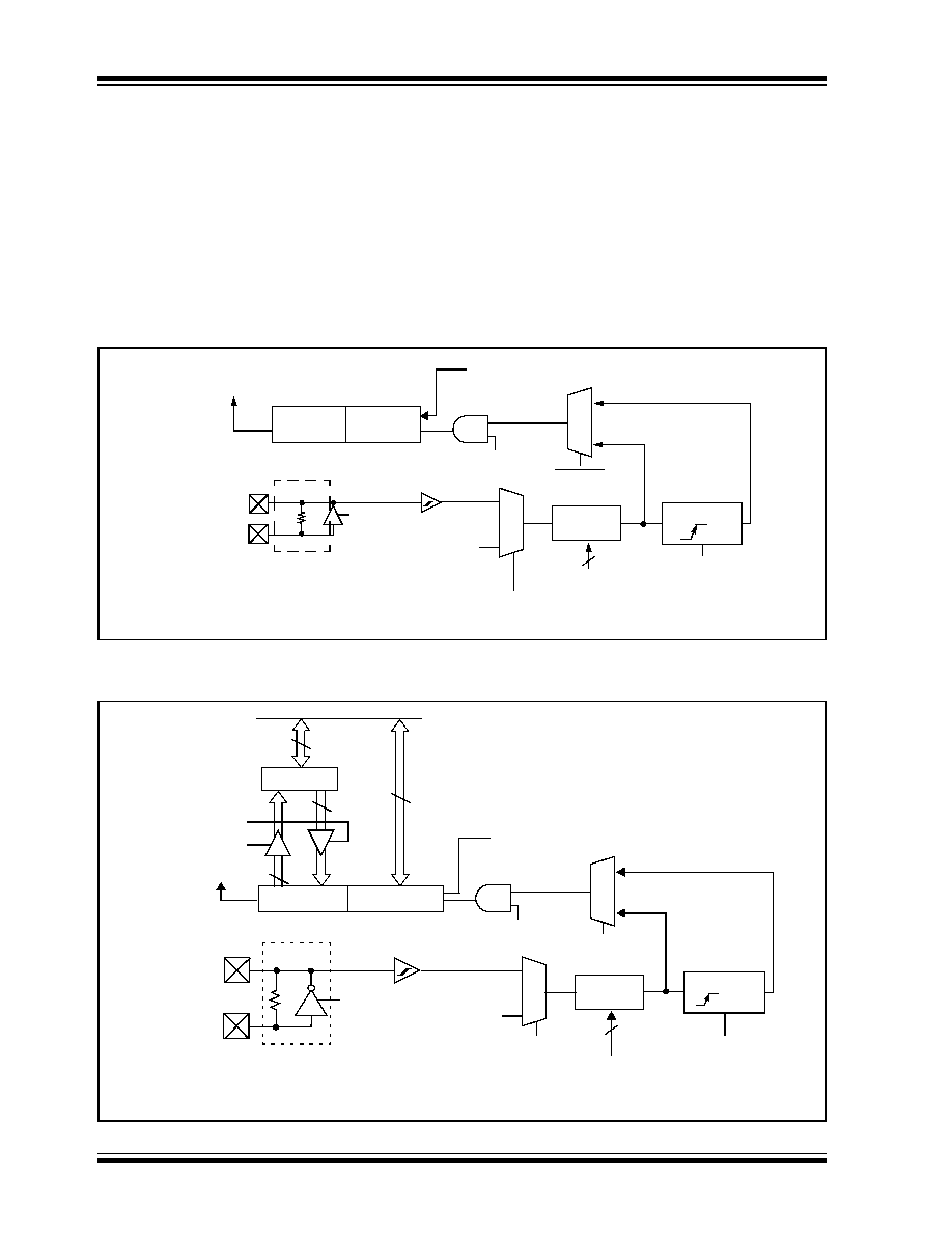
PIC18FXX8
DS41159B-page 112
Preliminary
2002 Microchip Technology Inc.
12.1
Timer1 Operation
Timer1 can operate in one of these modes:
� As a timer
� As a synchronous counter
� As an asynchronous counter
The Operating mode is determined by the clock select
bit, TMR1CS (T1CON register).
When TMR1CS is clear, Timer1 increments every
instruction cycle. When TMR1CS is set, Timer1 incre-
ments on every rising edge of the external clock input
or the Timer1 oscillator, if enabled.
When the Timer1 oscillator is enabled (T1OSCEN is
set), the RC1/T1OSI and RC0/T1OSO/T1CKI pins
become inputs. That is, the TRISC<1:0> value is
ignored.
Timer1 also has an internal "RESET input". This
RESET can be generated by the CCP module
(Section 15.1).
FIGURE 12-1:
TIMER1 BLOCK DIAGRAM
FIGURE 12-2:
TIMER1 BLOCK DIAGRAM: 16-BIT READ/WRITE MODE
TMR1H
TMR1L
T1SYNC
TMR1CS
T1CKPS1:T1CKPS0
SLEEP Input
F
OSC
/4
Internal
Clock
TMR1ON
On/Off
Prescaler
1, 2, 4, 8
Synchronize
det
1
0
0
1
Synchronized
Clock Input
2
TMR1IF
Overflow
TMR1
CLR
CCP Special Event Trigger
T1OSCEN
Enable
Oscillator
(1)
T1OSC
Interrupt
Flag bit
Note
1: When enable bit T1OSCEN is cleared, the inverter and feedback resistor are turned off. This reduces power drain.
T1OSI
T13CKI/T1OSO
Timer 1
TMR1L
T1OSC
T1SYNC
TMR1CS
T1CKPS1:T1CKPS0
SLEEP Input
T1OSCEN
Enable
Oscillator
(1)
TMR1IF
Overflow
Interrupt
F
OSC
/4
Internal
Clock
TMR1ON
On/Off
Prescaler
1, 2, 4, 8
Synchronize
det
1
0
0
1
Synchronized
Clock Input
2
T13CKI/T1OSO
T1OSI
TMR1
Flag bit
Note
1: When enable bit T1OSCEN is cleared, the inverter and feedback resistor are turned off. This reduces power drain.
high byte
Data Bus<7:0>
8
TMR1H
8
8
8
Read TMR1L
Write TMR1L
Special Event Trigger
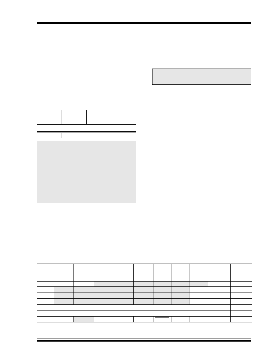
2002 Microchip Technology Inc.
Preliminary
DS41159B-page 113
PIC18FXX8
12.2
Timer1 Oscillator
A crystal oscillator circuit is built-in between pins T1OSI
(input) and T1OSO (amplifier output). It is enabled by
setting control bit T1OSCEN (T1CON register). The
oscillator is a low power oscillator rated up to 200 kHz.
It will continue to run during SLEEP. It is primarily
intended for a 32 kHz crystal. Table 12-1 shows the
capacitor selection for the Timer1 oscillator.
The user must provide a software time delay to ensure
proper start-up of the Timer1 oscillator.
12.3
Timer1 Interrupt
The TMR1 register pair (TMR1H:TMR1L) increments
from 0000h to FFFFh and rolls over to 0000h. The TMR1
Interrupt, if enabled, is generated on overflow, which is
latched in interrupt flag bit TMR1IF (PIR registers). This
interrupt can be enabled/disabled by setting/clearing
TMR1 interrupt enable bit TMR1IE (PIE registers).
12.4
Resetting Timer1 Using a CCP
Trigger Output
If the CCP module is configured in Compare mode to
generate a "special event trigger" (CCP1M3:CCP1M0 =
`
1011
'), this signal will reset Timer1 and start an A/D
conversion (if the A/D module is enabled).
Timer1 must be configured for either Timer or Synchro-
nized Counter mode to take advantage of this feature.
If Timer1 is running in Asynchronous Counter mode,
this RESET operation may not work.
In the event that a write to Timer1 coincides with a special
event trigger from CCP1, the write will take precedence.
In this mode of operation, the CCPR1H:CCPR1L registers
pair, effectively becomes the period register for Timer1.
12.5
Timer1 16-bit Read/Write Mode
Timer1 can be configured for 16-bit reads and writes
(see Figure 12-2). When the RD16 control bit (T1CON
register) is set, the address for TMR1H is mapped to a
buffer register for the high byte of Timer1. A read from
TMR1L will load the contents of the high byte of Timer1
into the Timer1 high byte buffer. This provides the user
with the ability to accurately read all 16 bits of Timer1,
without having to determine whether a read of the high
byte, followed by a read of the low byte is valid, due to
a rollover between reads.
A write to the high byte of Timer1 must also take place
through the TMR1H buffer register. Timer1 high byte is
updated with the contents of TMR1H when a write
occurs to TMR1L. This allows a user to write all 16 bits
to both the high and low bytes of Timer1 at once.
The high byte of Timer1 is not directly readable or writ-
able in this mode. All reads and writes must take place
through the Timer1 high byte buffer register. Writes to
TMR1H do not clear the Timer1 prescaler. The
prescaler is only cleared on writes to TMR1L.
TABLE 12-2:
REGISTERS ASSOCIATED WITH TIMER1 AS A TIMER/COUNTER
TABLE 12-1:
CAPACITOR SELECTION FOR
THE ALTERNATE
OSCILLATOR
Osc Type
Freq
C1
C2
LP
32 kHz
TBD
(1)
TBD
(1)
Crystal to be Tested:
32.768 kHz Epson C-001R32.768K-A
�
20 PPM
Note 1: Microchip suggests 33 pF as a starting
point in validating the oscillator circuit.
2: Higher capacitance increases the stability
of the oscillator, but also increases the
start-up time.
3: Since each resonator/crystal has its own
characteristics, the user should consult
the resonator/crystal manufacturer for
appropriate values of external components.
4: Capacitor values are for design guidance
only.
Note:
The special event triggers from the CCP1
module will not set interrupt flag bit
TMR1IF (PIR registers).
Name
Bit 7
Bit 6
Bit 5
Bit 4
Bit 3
Bit 2
Bit 1
Bit 0
Value on
POR, BOR
Value on
all other
RESETS
INTCON
GIE/GIEH PEIE/GIEL
TMR0IE
INT0IE
RBIE
TMR0IF
INT0IF
RBIF
0000 000x 0000 000u
PIR1
PSPIF
ADIF
RCIF
TXIF
SSPIF
CCP1IF
TMR2IF
TMR1IF
0000 0000 0000 0000
PIE1
PSPIE
ADIE
RCIE
TXIE
SSPIE
CCP1IE
TMR2IE
TMR1IE
0000 0000 0000 0000
IPR1
PSPIP
ADIP
RCIP
TXIP
SSPIP
CCP1IP
TMR2IP
TMR1IP
0000 0000 0000 0000
TMR1L
Holding Register for the Least Significant Byte of the 16-bit TMR1 Register
xxxx xxxx uuuu uuuu
TMR1H
Holding Register for the Most Significant Byte of the 16-bit TMR1 Register
xxxx xxxx uuuu uuuu
T1CON
RD16
--
T1CKPS1
T1CKPS0 T1OSCEN T1SYNC TMR1CS TMR1ON
0-00 0000 u-uu uuuu
Legend:
x
= unknown,
u
= unchanged,
-
= unimplemented, read as '0'. Shaded cells are not used by the Timer1 module.

PIC18FXX8
DS41159B-page 114
Preliminary
2002 Microchip Technology Inc.
NOTES:
2002 Microchip Technology Inc.
Preliminary
DS41159B-page 115
PIC18FXX8
13.0
TIMER2 MODULE
The Timer2 module timer has the following features:
� 8-bit timer (TMR2 register)
� 8-bit period register (PR2)
� Readable and writable (both registers)
� Software programmable prescaler (1:1, 1:4, 1:16)
� Software programmable postscaler (1:1 to 1:16)
� Interrupt on TMR2 match of PR2
� SSP module optional use of TMR2 output to
generate clock shift
Register 13-1 shows the Timer2 Control register.
Timer2 can be shut-off by clearing control bit TMR2ON
(T2CON register) to minimize power consumption.
Figure 13-1 is a simplified block diagram of the Timer2
module. The prescaler and postscaler selection of
Timer2 are controlled by this register.
13.1
Timer2 Operation
Timer2 can be used as the PWM time-base for the
PWM mode of the CCP module. The TMR2 register is
readable and writable, and is cleared on any device
RESET. The input clock (F
OSC
/4) has a prescale option
of 1:1, 1:4, or 1:16, selected by control bits
T2CKPS1:T2CKPS0 (T2CON Register). The match
output of TMR2 goes through a 4-bit postscaler (which
gives a 1:1 to 1:16 scaling inclusive) to generate a
TMR2 interrupt (latched in flag bit TMR2IF, PIR
registers).
The prescaler and postscaler counters are cleared
when any of the following occurs:
� A write to the TMR2 register
� A write to the T2CON register
� Any device RESET (Power-on Reset, MCLR
Reset, Watchdog Timer Reset, or Brown-out
Reset)
TMR2 is not cleared when T2CON is written.
REGISTER 13-1:
T2CON REGISTER
Note:
Timer2 is disabled on POR.
U-0
R/W-0
R/W-0
R/W-0
R/W-0
R/W-0
R/W-0
R/W-0
--
TOUTPS3 TOUTPS2 TOUTPS1 TOUTPS0
TMR2ON
T2CKPS1
T2CKPS0
bit 7
bit 0
bit 7
Unimplemented: Read as '0'
bit 6-3
TOUTPS3:TOUTPS0: Timer2 Output Postscale Select bits
0000
= 1:1 Postscale
0001
= 1:2 Postscale
�
�
�
1111
= 1:16 Postscale
bit 2
TMR2ON: Timer2 On bit
1
= Timer2 is on
0
= Timer2 is off
bit 1-0
T2CKPS1:T2CKPS0: Timer2 Clock Prescale Select bits
00
= Prescaler is 1
01
= Prescaler is 4
1x
= Prescaler is 16
Legend:
R = Readable bit
W = Writable bit
U = Unimplemented bit, read as `0'
- n = Value at POR
'1' = Bit is set
'0' = Bit is cleared
x = Bit is unknown
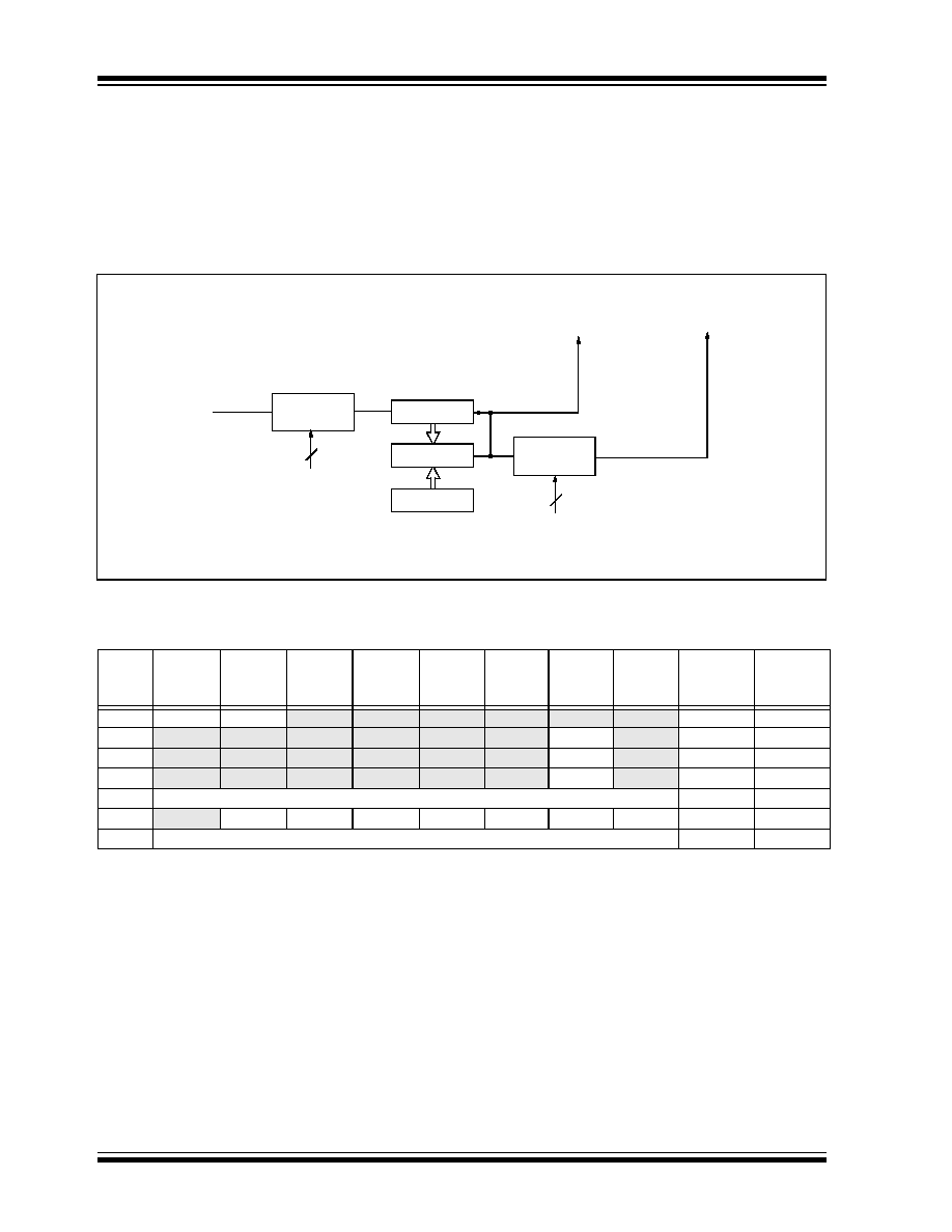
PIC18FXX8
DS41159B-page 116
Preliminary
2002 Microchip Technology Inc.
13.2
Timer2 Interrupt
The Timer2 module has an 8-bit period register, PR2.
Timer2 increments from 00h until it matches PR2 and
then resets to 00h on the next increment cycle. PR2 is
a readable and writable register. The PR2 register is
initialized to FFh upon RESET.
13.3
Output of TMR2
The output of TMR2 (before the postscaler) is a clock
input to the Synchronous Serial Port module, which
optionally uses it to generate the shift clock.
FIGURE 13-1:
TIMER2 BLOCK DIAGRAM
TABLE 13-1:
REGISTERS ASSOCIATED WITH TIMER2 AS A TIMER/COUNTER
Comparator
TMR2
Sets Flag
TMR2
Output
(1)
RESET
Postscaler
Prescaler
PR2
2
F
OSC
/4
1:1 to 1:16
1:1, 1:4, 1:16
EQ
4
bit TMR2IF
Note
1: TMR2 register output can be software selected by the SSP Module as a baud clock.
TOUTPS3:TOUTPS0
T2CKPS1:T2CKPS0
Name
Bit 7
Bit 6
Bit 5
Bit 4
Bit 3
Bit 2
Bit 1
Bit 0
Value on
POR, BOR
Value on
all other
RESETS
INTCON GIE/GIEH PEIE/GIEL
TMR0IE
INT0IE
RBIE
TMR0IF
INT0IF
RBIF
0000 000x 0000 000u
PIR1
PSPIF
ADIF
RCIF
TXIF
SSPIF
CCP1IF
TMR2IF
TMR1IF
0000 0000 0000 0000
PIE1
PSPIE
ADIE
RCIE
TXIE
SSPIE
CCP1IE
TMR2IE
TMR1IE
0000 0000 0000 0000
IPR1
PSPIP
ADIP
RCIP
TXIP
SSPIP
CCP1IP
TMR2IP
TMR1IP
0000 0000 0000 0000
TMR2
Timer2 Module Register
0000 0000 0000 0000
T2CON
--
TOUTPS3 TOUTPS2 TOUTPS1 TOUTPS0 TMR2ON T2CKPS1 T2CKPS0
-000 0000 -000 0000
PR2
Timer2 Period Register
1111 1111 1111 1111
Legend:
x
= unknown,
u
= unchanged,
-
= unimplemented, read as '0'. Shaded cells are not used by the Timer2 module.
2002 Microchip Technology Inc.
Preliminary
DS41159B-page 117
PIC18FXX8
14.0
TIMER3 MODULE
The Timer3 module timer/counter has the following
features:
� 16-bit timer/counter
(Two 8-bit registers: TMR3H and TMR3L)
� Readable and writable (both registers)
� Internal or external clock select
� Interrupt-on-overflow from FFFFh to 0000h
� RESET from CCP1/ECCP1 module trigger
Figure 14-1 is a simplified block diagram of the Timer3
module.
Register 14-1 shows the Timer3 Control Register. This
register controls the Operating mode of the Timer3
module and sets the CCP1 and ECCP1 clock source.
Register 12-1 shows the Timer1 Control register. This
register controls the Operating mode of the Timer1
module, as well as contains the Timer1 oscillator
enable bit (T1OSCEN), which can be a clock source for
Timer3.
REGISTER 14-1:
T3CON REGISTER
Note:
Timer3 is disabled on POR.
R/W-0
R/W-0
R/W-0
R/W-0
R/W-0
R/W-0
R/W-0
R/W-0
RD16
T3ECCP1 T3CKPS1 T3CKPS0
T3CCP1
T3SYNC
TMR3CS
TMR3ON
bit 7
bit 0
bit 7
RD16: 16-bit Read/Write Mode Enable bit
1
= Enables register read/write of Timer3 in one 16-bit operation
0
= Enables register read/write of Timer3 in two 8-bit operations
bit 6,3
T3ECCP1:T3CCP1: Timer3 and Timer1 to CCP1/ECCP1 Enable bits
1x
=Timer3 is the clock source for compare/capture CCP1 and ECCP1 modules
01
=Timer3 is the clock source for compare/capture of ECCP1,
Timer1 is the clock source for compare/capture of CCP1
00
= Timer1 is the clock source for compare/capture CCP1 and ECCP1 modules
bit 5-4
T3CKPS1:T3CKPS0: Timer3 Input Clock Prescale Select bits
11
= 1:8 Prescale value
10
= 1:4 Prescale value
01
= 1:2 Prescale value
00
= 1:1 Prescale value
bit 2
T3SYNC: Timer3 External Clock Input Synchronization Control bit
(Not usable if the system clock comes from Timer1/Timer3)
When TMR3CS = 1:
1
= Do not synchronize external clock input
0
= Synchronize external clock input
When TMR3CS = 0:
This bit is ignored. Timer3 uses the internal clock when TMR3CS = 0.
bit 1
TMR3CS: Timer3 Clock Source Select bit
1
= External clock input from Timer1 oscillator or T1CKI (on the rising edge after the first falling edge)
0
= Internal clock (F
OSC
/4)
bit 0
TMR3ON: Timer3 On bit
1
= Enables Timer3
0
= Stops Timer3
Legend:
R = Readable bit
W = Writable bit
U = Unimplemented bit, read as `0'
- n = Value at POR
'1' = Bit is set
'0' = Bit is cleared
x = Bit is unknown
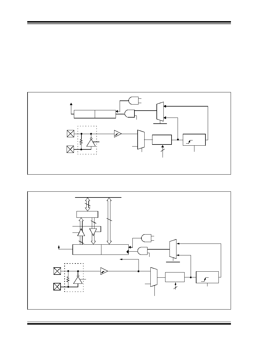
PIC18FXX8
DS41159B-page 118
Preliminary
2002 Microchip Technology Inc.
14.1
Timer3 Operation
Timer3 can operate in one of these modes:
� As a timer
� As a synchronous counter
� As an asynchronous counter
The Operating mode is determined by the clock select
bit, TMR3CS (T3CON register).
When TMR3CS = 0, Timer3 increments every instruc-
tion cycle. When TMR3CS = 1, Timer3 increments on
every rising edge of the Timer1 external clock input, or
the Timer1 oscillator, if enabled.
When the Timer1 oscillator is enabled (T1OSCEN is set),
the RC1/T1OSI and RC0/T1OSO/T1CKI pins become
inputs. That is, the TRISC<1:0> value is ignored.
Timer3 also has an internal "RESET input". This
RESET can be generated by the CCP module
(Section 15.1).
FIGURE 14-1:
TIMER3 BLOCK DIAGRAM
FIGURE 14-2:
TIMER3 BLOCK DIAGRAM CONFIGURED IN 16-BIT READ/WRITE MODE
TMR3H
TMR3L
T1OSC
T3SYNC
TMR3CS
T3CKPS1:T3CKPS0
SLEEP Input
T1OSCEN
Enable
Oscillator
(1)
TMR3IF
Overflow
Interrupt
F
OSC
/4
Internal
Clock
TMR3ON
On/Off
Prescaler
1, 2, 4, 8
Synchronize
det
1
0
0
1
Synchronized
Clock Input
2
T1OSO/
T1OSI
Flag bit
Note
1: When enable bit T1OSCEN is cleared, the inverter and feedback resistor are turned off. This eliminates power drain.
T13CKI
CCP Special Trigger
T3CCPx
CLR
TMR3L
T1OSC
T3SYNC
TMR3CS
T3CKPS1:T3CKPS0
SLEEP Input
T1OSCEN
Enable
Oscillator
(1)
F
OSC
/4
Internal
Clock
TMR3ON
On/Off
Prescaler
1, 2, 4, 8
Synchronize
det
1
0
0
1
Synchronized
Clock Input
2
T1OSO/
T1OSI
TMR3
T13CKI
CLR
CCP Special Trigger
T3CCPx
To Timer1 Clock Input
Note
1: When the T1OSCEN bit is cleared, the inverter and feedback resistor are turned off. This eliminates power drain.
TMR3H
Data Bus<7:0>
8
TMR3H
8
8
8
Read TMR3L
Write TMR3L
TMR3IF Overflow
Interrupt Flag
bit
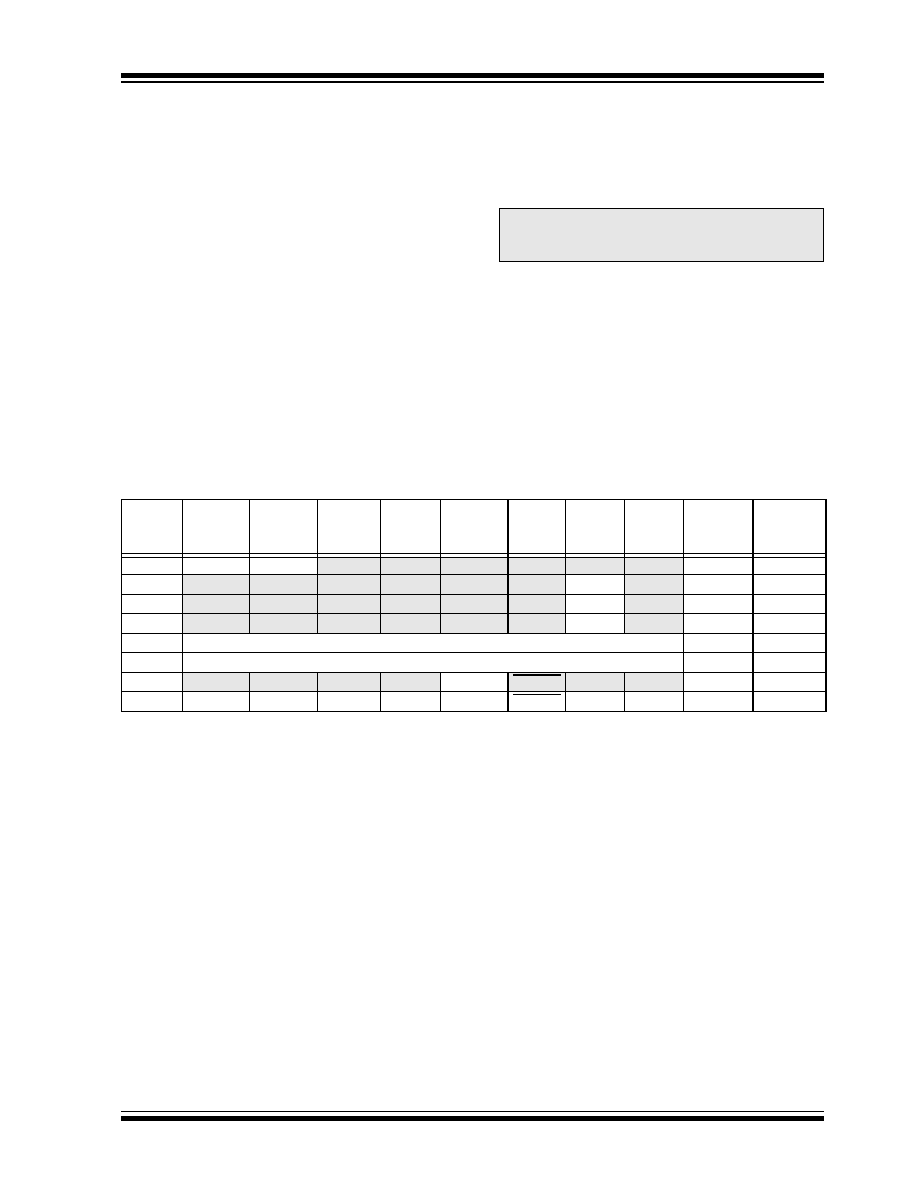
2002 Microchip Technology Inc.
Preliminary
DS41159B-page 119
PIC18FXX8
14.2
Timer1 Oscillator
The Timer1 oscillator may be used as the clock source
for Timer3. The Timer1 oscillator is enabled by setting
the T1OSCEN bit (T1CON Register). The oscillator is a
low power oscillator rated up to 200 kHz. Refer to
Section 12.0, Timer1 Module for Timer1 oscillator
details.
14.3
Timer3 Interrupt
The TMR3 Register pair (TMR3H:TMR3L) increments
from 0000h to FFFFh and rolls over to 0000h. The TMR3
Interrupt, if enabled, is generated on overflow, which is
latched in interrupt flag bit TMR3IF (PIR registers). This
interrupt can be enabled/disabled by setting/clearing
TMR3 interrupt enable bit TMR3IE (PIE registers).
14.4
Resetting Timer3 Using a CCP
Trigger Output
If the CCP module is configured in Compare mode to
generate a "special event trigger" (CCP1M3:CCP1M0
=
1011
), this signal will reset Timer3.
Timer3 must be configured for either Timer or Synchro-
nized Counter mode to take advantage of this feature. If
Timer3 is running in Asynchronous Counter mode, this
RESET operation may not work. In the event that a write
to Timer3 coincides with a special event trigger from
CCP1, the write will take precedence. In this mode of
operation, the CCPR1H:CCPR1L registers pair
becomes the period register for Timer3. Refer to
Section 15.0, "Capture/Compare/PWM (CCP) Modules
for CCP details.
TABLE 14-1:
REGISTERS ASSOCIATED WITH TIMER3 AS A TIMER/COUNTER
Note:
The special event triggers from the CCP
module will not set interrupt flag bit
TMR3IF (PIR registers).
Name
Bit 7
Bit 6
Bit 5
Bit 4
Bit 3
Bit 2
Bit 1
Bit 0
Value on
POR,
BOR
Value on
all other
RESETS
INTCON
GIE/ GIEH PEIE/GIEL
TMR0IE
INT0IE
RBIE
TMR0IF
INT0IF
RBIF
0000 000x 0000 000u
PIR2
--
CMIF
--
EEIF
BCLIF
LVDIF
TMR3IF
ECCP1IF
-0-0 0000 -0-0 0000
PIE2
--
CMIE
--
EEIE
BCLIE
LVDIE
TMR3IE
ECCP1IE
-0-0 0000 -0-0 0000
IPR2
--
CMIP
--
EEIP
BCLIP
LVDIP
TMR3IP
ECCP1IP
-0-0 0000 -0-0 0000
TMR3L
Holding Register for the Least Significant Byte of the 16-bit TMR3 Register
xxxx xxxx uuuu uuuu
TMR3H
Holding Register for the Most Significant Byte of the 16-bit TMR3 Register
xxxx xxxx uuuu uuuu
T1CON
RD16
--
T1CKPS1 T1CKPS0 T1OSCEN T1SYNC TMR1CS TMR1ON
0-00 0000 u-uu uuuu
T3CON
RD16
T3ECCP1
T3CKPS1 T3CKPS0
T3CCP1
T3SYNC TMR3CS TMR3ON
0000 0000 uuuu uuuu
Legend:
x
= unknown,
u
= unchanged,
-
= unimplemented, read as '0'. Shaded cells are not used by the Timer1 module.

PIC18FXX8
DS41159B-page 120
Preliminary
2002 Microchip Technology Inc.
NOTES:
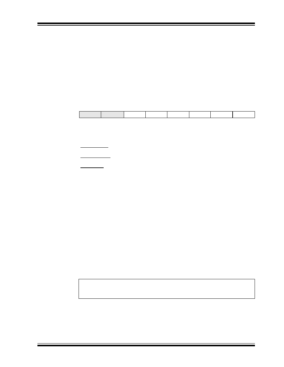
2002 Microchip Technology Inc.
Preliminary
DS41159B-page 121
PIC18FXX8
15.0
CAPTURE/COMPARE/PWM
(CCP) MODULES
The CCP (Capture/Compare/PWM) module contains a
16-bit register that can operate as a 16-bit capture reg-
ister, as a 16-bit compare register, or as a PWM Duty
Cycle register.
The operation of the CCP module is identical to that of
the ECCP module (discussed in detail in Section 16.0),
with two exceptions. The CCP module has a Capture
special event trigger that can be used as a message
received time stamp for the CAN module (refer to
Section 19.0, CAN Module for CAN operation), which
the ECCP module does not. The ECCP module, on the
other hand, has enhanced PWM functionality and auto
shutdown capability. Aside from these, the operation of
the module described in the this section is the same as
the ECCP .
The control register for the CCP module is shown in
Register 15-1. Table 15-2 (following page) details the
interactions of the CCP and ECCP modules.
REGISTER 15-1:
CCP1CON REGISTER
U-0
U-0
R/W-0
R/W-0
R/W-0
R/W-0
R/W-0
R/W-0
--
--
DC1B1
DC1B0
CCP1M3
CCP1M2
CCP1M1
CCP1M0
bit 7
bit 0
bit 7-6
Unimplemented: Read as '0'
bit 5-4
DCxB1:DCxB0: PWM Duty Cycle bit1 and bit0
Capture mode:
Unused
Compare mode:
Unused
PWM mode:
These bits are the two LSbs (bit1 and bit0) of the 10-bit PWM duty cycle. The upper eight bits
(DCx9:DCx2) of the duty cycle are found in CCPRxL.
bit 3-0
CCPxM3:CCPxM0: CCPx Mode Select bits
0000
= Capture/Compare/PWM off (resets CCPx module)
0001
= Reserved
0010
= Compare mode, toggle output on match (CCPxIF bit is set)
0011
= Capture mode, CAN message received (CCP1 only)
0100
= Capture mode, every falling edge
0101
= Capture mode, every rising edge
0110
= Capture mode, every 4th rising edge
0111
= Capture mode, every 16th rising edge
1000
= Compare mode, initialize CCP pin Low, on compare match force CCP pin High
(CCPIF bit is set)
1001
= Compare mode, initialize CCP pin High, on compare match force CCP pin Low
(CCPIF bit is set)
1010
= Compare mode, CCP pin is unaffected
(CCPIF bit is set)
1011
= Compare mode, trigger special event (CCP1IF bit is set; CCP resets TMR1 or TMR3
and starts an A/D conversion, if the A/D module is enabled)
11xx
= PWM mode
Legend:
R = Readable bit
W = Writable bit
U = Unimplemented bit, read as `0'
- n = Value at POR
'1' = Bit is set
'0' = Bit is cleared
x = Bit is unknown

PIC18FXX8
DS41159B-page 122
Preliminary
2002 Microchip Technology Inc.
15.1
CCP1 Module
Capture/Compare/PWM Register1 (CCPR1) is com-
prised of two 8-bit registers: CCPR1L (low byte) and
CCPR1H (high byte). The CCP1CON register controls
the operation of CCP1. All are readable and writable.
Table 15-1 shows the timer resources of the CCP
module modes.
TABLE 15-1:
CCP1 MODE - TIMER
RESOURCE
15.2
Capture Mode
In Capture mode, CCPR1H:CCPR1L captures the
16-bit value of the TMR1 or TMR3 register when an
event occurs on pin RC2/CCP1. An event is defined as:
� every falling edge
� every rising edge.
� every 4th rising edge
� every 16th rising edge
An event is selected by control bits CCP1M3:CCP1M0
(CCP1CON<3:0>). When a capture is made, the inter-
rupt request flag bit CCP1IF (PIR registers) is set. It
must be cleared in software. If another capture occurs
before the value in register CCPR1 is read, the old
captured value will be lost.
15.2.1
CCP PIN CONFIGURATION
In Capture mode, the RC2/CCP1 pin should be
configured as an input by setting the TRISC<2> bit.
15.2.2
TIMER1/TIMER3 MODE SELECTION
The timers used with the capture feature (either Timer1
and/or Timer3) must be running in Timer mode or Syn-
chronized Counter mode. In Asynchronous Counter
mode, the capture operation may not work. The timer
used with each CCP module is selected in the T3CON
register.
TABLE 15-2:
INTERACTION OF CCP1 AND ECCP1 MODULES
CCP1 Mode
Timer Resource
Capture
Compare
PWM
Timer1 or Timer3
Timer1 or Timer3
Timer2
Note:
If the RC2/CCP1 is configured as an out-
put, a write to the port can cause a capture
condition.
CCP1
Mode
ECCP1
Mode
Interaction
Capture
Capture
TMR1 or TMR3 time-base. Time-base can be different for each CCP.
Capture
Compare
The compare could be configured for the special event trigger, which clears either TMR1
or TMR3, depending upon which time-base is used.
Compare
Compare
The compare(s) could be configured for the special event trigger, which clears TMR1 or
TMR3, depending upon which time-base is used.
PWM
PWM
The PWMs will have the same frequency and update rate (TMR2 interrupt).
PWM
Capture
None.
PWM
Compare
None.
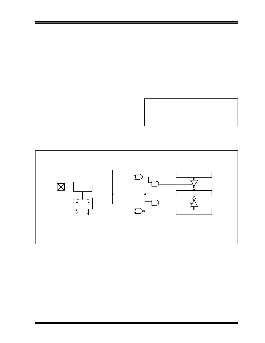
2002 Microchip Technology Inc.
Preliminary
DS41159B-page 123
PIC18FXX8
15.2.3
SOFTWARE INTERRUPT
When the Capture mode is changed, a false capture
interrupt may be generated. The user should keep bit
CCP1IE (PIE registers) clear to avoid false interrupts
and should clear the flag bit CCP1IF, following any
such change in Operating mode.
15.2.4
CCP1 PRESCALER
There are four prescaler settings, specified by bits
CCP1M3:CCP1M0. Whenever the CCP1 module is
turned off, or the CCP1 module is not in Capture mode,
the prescaler counter is cleared. This means that any
RESET will clear the prescaler counter.
Switching from one capture prescaler to another may
generate an interrupt. Also, the prescaler counter will
not be cleared; therefore, the first capture may be from
a non-zero prescaler. Example 15-1 shows the recom-
mended method for switching between capture pres-
calers. This example also clears the prescaler counter
and will not generate the "false" interrupt.
15.2.5
CAN MESSAGE TIME-STAMP
The CAN capture event occurs when a message is
received in either of the receive buffers. The CAN mod-
ule provides a rising edge to the CCP1 module to
cause a capture event. This feature is provided to
time-stamp the received CAN messages.
This feature is enabled by setting the CANCAP bit of
the CAN I/O control register (CIOCON<4>). The mes-
sage receive signal from the CAN module then takes
the place of the events on RC2/CCP1.
EXAMPLE 15-1:
CHANGING BETWEEN
CAPTURE PRESCALERS
FIGURE 15-1:
CAPTURE MODE OPERATION BLOCK DIAGRAM
CLRF
CCP1CON, F
; Turn CCP module off
MOVLW
NEW_CAPT_PS
; Load WREG with the
; new prescaler mode
; value and CCP ON
MOVWF
CCP1CON
; Load CCP1CON with
; this value
Note: I/O pins have diode protection to V
DD
and V
SS
.
CCPR1H
CCPR1L
TMR1H
TMR1L
Set Flag bit CCP1IF
(PIR1<2>)
TMR3
Enable
Qs
CCP1CON<3:0>
CCP1 pin
Prescaler
�
1, 4, 16
and
Edge Detect
TMR3H
TMR3L
TMR1
Enable
T3ECCP1
T3CCP1
T3ECCP1
T3CCP1
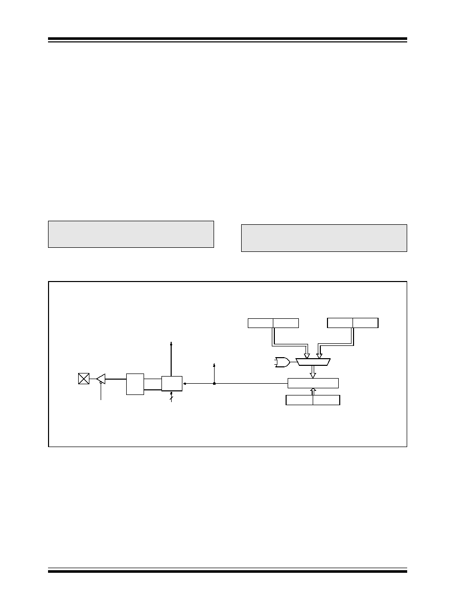
PIC18FXX8
DS41159B-page 124
Preliminary
2002 Microchip Technology Inc.
15.3
Compare Mode
In Compare mode, the 16-bit CCPR1 and ECCPR1
register value is constantly compared against either the
TMR1 register pair value, or the TMR3 register pair
value. When a match occurs, the CCP1 pin can have
one of the following actions:
� Driven high
� Driven low
� Toggle output (high to low or low to high)
� Remains unchanged
The action on the pin is based on the value of control
bits CCP1M3:CCP1M0. At the same time, interrupt flag
bit CCP1IF is set.
15.3.1
CCP1 PIN CONFIGURATION
The user must configure the CCP1 pin as an output by
clearing the appropriate TRISC bit.
15.3.2
TIMER1/TIMER3 MODE SELECTION
Timer1 and/or Timer3 must be running in Timer mode,
or Synchronized Counter mode, if the CCP module is
using the compare feature. In Asynchronous Counter
mode, the compare operation may not work.
15.3.3
SOFTWARE INTERRUPT MODE
When Generate Software Interrupt is chosen, the
CCP1 pin is not affected. Only a CCP interrupt is
generated (if enabled).
15.3.4
SPECIAL EVENT TRIGGER
In this mode, an internal hardware trigger is generated,
which may be used to initiate an action.
The special event trigger output of CCP1 resets either
the TMR1 or TMR3 register pair. Additionally, the
ECCP1 Special Event Trigger will start an A/D
conversion, if the A/D module is enabled.
FIGURE 15-2:
COMPARE MODE OPERATION BLOCK DIAGRAM
Note:
Clearing the CCP1CON register will force
the CCP1 compare output latch to the
default low level. This is not the data latch.
Note:
The Special Event Trigger from the ECCP1
module will not set the Timer1 or Timer3
interrupt flag bits.
Special Event Trigger will:
Reset Timer1 or Timer3 (but not set Timer1 or Timer3 Interrupt Flag bit)
Set bit GO/DONE, which starts an A/D conversion (ECCP1 only)
Note: I/O pins have diode protection to V
DD
and V
SS
.
TMR1H
TMR1L
TMR3H
TMR3L
CCPR1H CCPR1L
Comparator
T3ECCP1
T3CCP1
Q
S
R
Output
Logic
Special Event Trigger
Match
CCP1
CCP1CON<3:0>
Mode Select
Output Enable
0
1
Set Flag bit CCP1IF
(PIR1<2>)
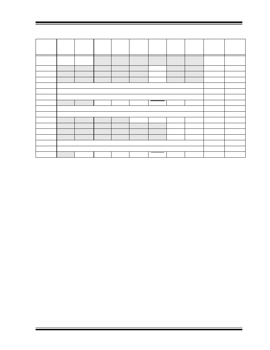
2002 Microchip Technology Inc.
Preliminary
DS41159B-page 125
PIC18FXX8
TABLE 15-3:
REGISTERS ASSOCIATED WITH CAPTURE, COMPARE, TIMER1 AND TIMER3
Name
Bit 7
Bit 6
Bit 5
Bit 4
Bit 3
Bit 2
Bit 1
Bit 0
Value on
POR, BOR
Value on
all other
RESETS
INTCON
GIE/
GIEH
PEIE/
GIEL
TMR0IE
INT0IE
RBIE
TMR0IF
INT0IF
RBIF
0000 000x 0000 000u
PIR1
PSPIF
ADIF
RCIF
TXIF
SSPIF
CCP1IF
TMR2IF
TMR1IF
0000 0000 0000 0000
PIE1
PSPIE
ADIE
RCIE
TXIE
SSPIE
CCP1IE
TMR2IE
TMR1IE
0000 0000 0000 0000
IPR1
PSPIP
ADIP
RCIP
TXIP
SSPIP
CCP1IP
TMR2IP
TMR1IP
0000 0000 0000 0000
TRISD
PORTD Data Direction Register
1111 1111 1111 1111
TMR1L
Holding Register for the Least Significant Byte of the 16-bit TMR1 Register
xxxx xxxx uuuu uuuu
TMR1H
Holding Register for the Most Significant Byte of the 16-bit TMR1 Register
xxxx xxxx uuuu uuuu
T1CON
RD16
--
T1CKPS1 T1CKPS0 T1OSCEN
T1SYNC
TMR1CS
TMR1ON
0-00 0000 u-uu uuuu
CCPR1L
Capture/Compare/PWM Register1 (LSB)
xxxx xxxx uuuu uuuu
CCPR1H
Capture/Compare/PWM Register1 (MSB)
xxxx xxxx uuuu uuuu
CCP1CON
--
--
DC1B1
DC1B0
CCP1M3
CCP1M2
CCP1M1
CCP1M0
--00 0000 --00 0000
PIR2
--
CMIF
--
EEIF
BCLIF
LVDIF
TMR3IF
ECCP1IF
-0-0 0000 -0-0 0000
PIE2
--
CMIE
--
EEIE
BCLIE
LVDIE
TMR3IE
ECCP1IE
-0-0 0000 -0-0 0000
IPR2
--
CMIP
--
EEIP
BCLIP
LVDIP
TMR3IP
ECCP1IP
-0-0 0000 -0-0 0000
TMR3L
Holding Register for the Least Significant Byte of the 16-bit TMR3 Register
xxxx xxxx uuuu uuuu
TMR3H
Holding Register for the Most Significant Byte of the 16-bit TMR3 Register
xxxx xxxx uuuu uuuu
T3CON
RD16
T3ECCP1
T3CKPS1 T3CKPS0
T3CCP1
T3SYNC
TMR3CS
TMR3ON
0000 0000 uuuu uuuu
Legend:
x
= unknown,
u
= unchanged,
-
= unimplemented, read as '0'. Shaded cells are not used by Capture and Timer1.
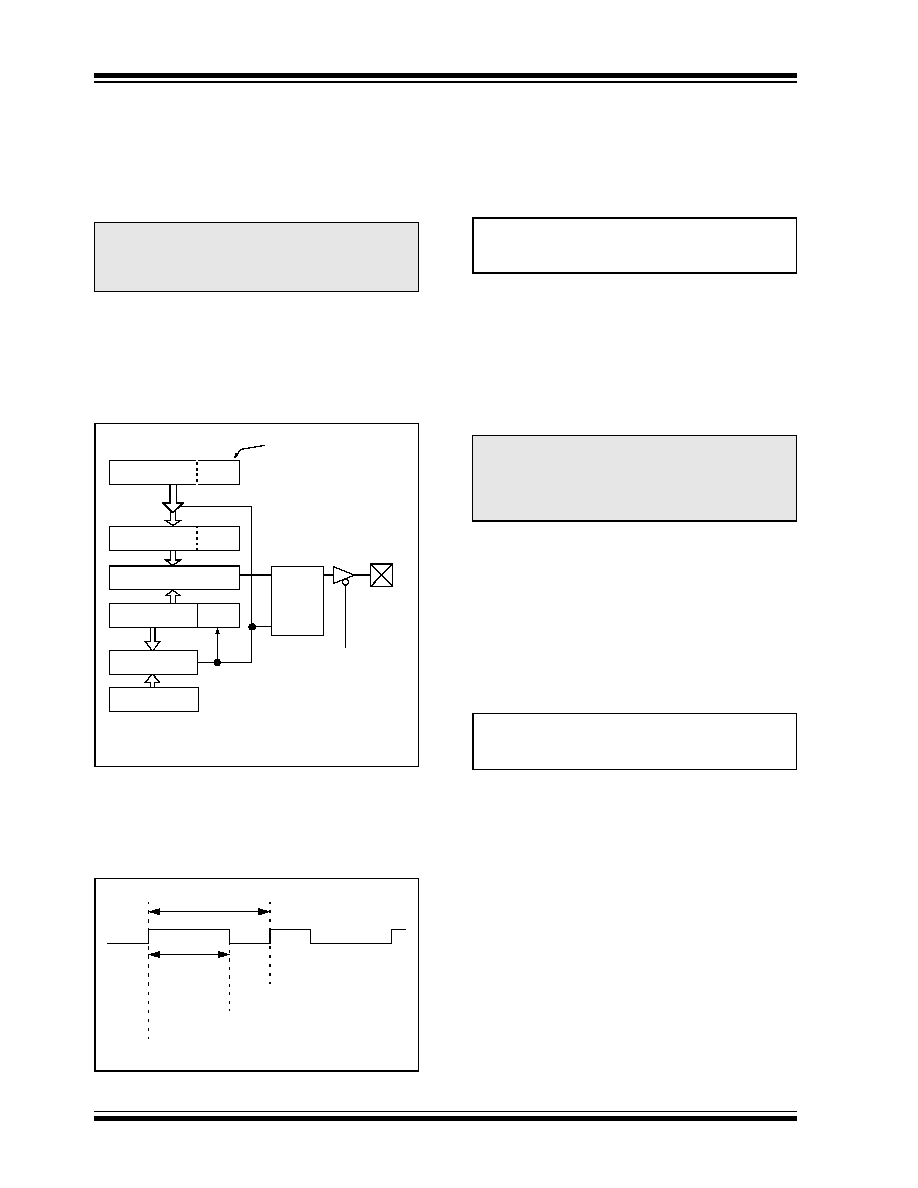
PIC18FXX8
DS41159B-page 126
Preliminary
2002 Microchip Technology Inc.
15.4
PWM Mode
In Pulse Width Modulation (PWM) mode, the CCP1 pin
produces up to a 10-bit resolution PWM output. Since
the CCP1 pin is multiplexed with the PORTC data latch,
the TRISC<2> bit must be cleared to make the CCP1
pin an output.
Figure 15-3 shows a simplified block diagram of the
CCP module in PWM mode.
For a step-by-step procedure on how to set up the CCP
module for PWM operation, see Section 15.4.3.
FIGURE 15-3:
SIMPLIFIED PWM BLOCK
DIAGRAM
A PWM output (Figure 15-4) has a time-base (period)
and a time that the output stays high (duty cycle). The
frequency of the PWM is the inverse of the period
(1/period).
FIGURE 15-4:
PWM OUTPUT
15.4.1
PWM PERIOD
The PWM period is specified by writing to the PR2 reg-
ister. The PWM period can be calculated using the
following formula.
EQUATION 15-1:
PWM frequency is defined as 1 / [PWM period].
When TMR2 is equal to PR2, the following three events
occur on the next increment cycle:
� TMR2 is cleared
� The CCP1 pin is set (exception: if PWM duty
cycle = 0%, the CCP1 pin will not be set)
� The PWM duty cycle is latched from CCPR1L into
CCPR1H
15.4.2
PWM DUTY CYCLE
The PWM duty cycle is specified by writing to the
CCPR1L register and to the CCP1CON<5:4> bits. Up
to 10-bit resolution is available. The CCPR1L contains
the eight MSbs and the CCP1CON<5:4> contains the
two LSbs. This 10-bit value is represented by
CCPR1L:CCP1CON<5:4>. The following equation is
used to calculate the PWM duty cycle in time.
EQUATION 15-2:
CCPR1L and CCP1CON<5:4> can be written to at any
time, but the duty cycle value is not latched into
CCPR1H until after a match between PR2 and TMR2
occurs (i.e., the period is complete). In PWM mode,
CCPR1H is a read only register.
The CCPR1H register and a 2-bit internal latch are
used to double buffer the PWM duty cycle. This double
buffering is essential for glitchless PWM operation.
When the CCPR1H and 2-bit latch match TMR2, con-
catenated with an internal 2-bit Q clock, or 2 bits of the
TMR2 prescaler, the CCP1 pin is cleared.
Note:
Clearing the CCP1CON register will force
the CCP1 PWM output latch to the default
low level. This is not the PORTC I/O data
latch.
CCPR1L (Master)
CCPR1H (Slave)
Comparator
TMR2
PR2
(Note 1)
R
Q
S
Duty Cycle Registers
CCP1CON<5:4>
Clear Timer,
Set CCP1 pin and
latch D.C.
TRISC<2>
RC2/CCP1
Note 1: 8-bit timer is concatenated with 2-bit internal Q clock,
or 2 bits of the prescaler, to create 10-bit time-base.
Comparator
Period
Duty Cycle
TMR2 = PR2
TMR2 = Duty Cycle
TMR2 = PR2
Note:
The Timer2 postscaler (see Section 13.0)
is not used in the determination of the
PWM frequency. The postscaler could be
used to have a servo update rate at a
different frequency than the PWM output.
PWM period =
[(PR2) + 1] � 4 � T
OSC
�
(TMR2 prescale value)
PWM duty cycle =(CCPR1L:CCP1CON<5:4>) �
T
OSC
� (TMR2 prescale value)
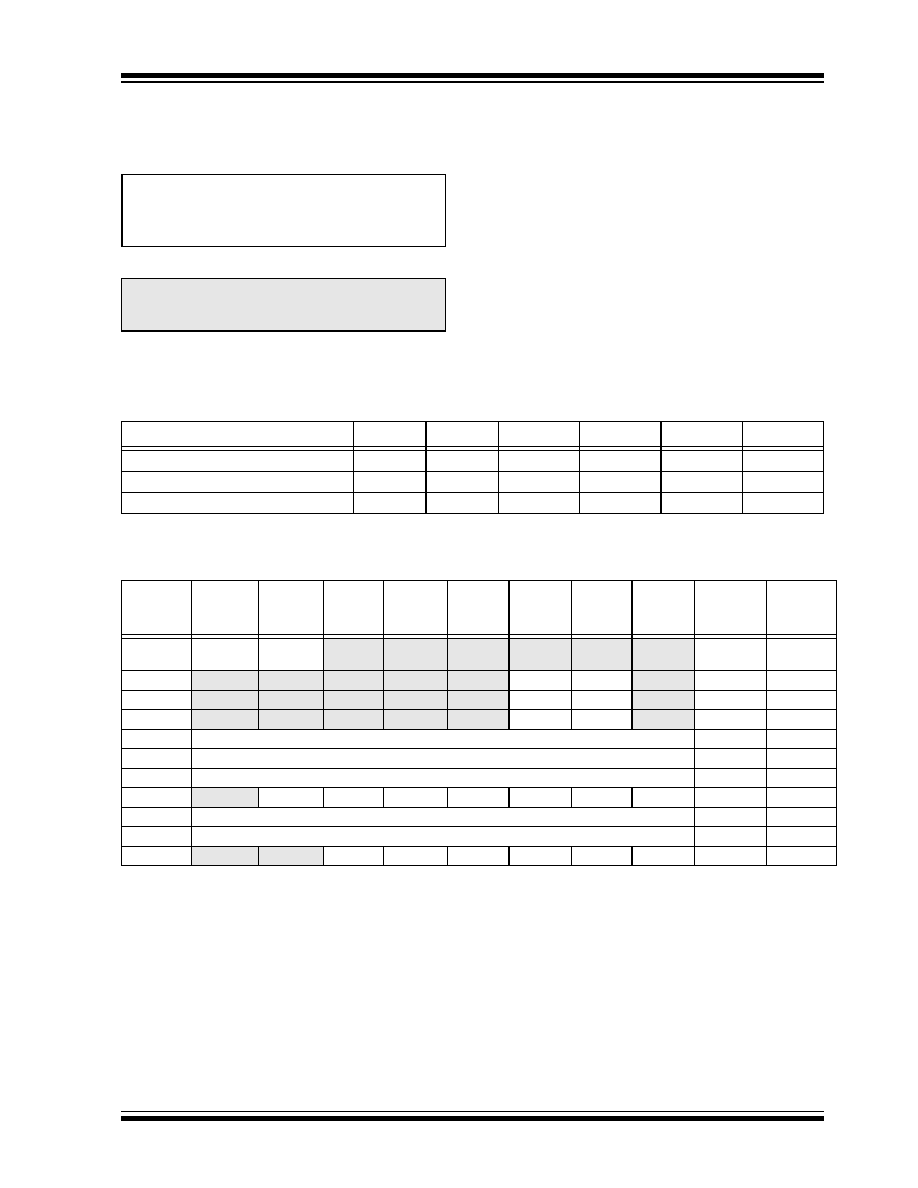
2002 Microchip Technology Inc.
Preliminary
DS41159B-page 127
PIC18FXX8
The maximum PWM resolution (bits) for a given PWM
frequency is given by the following equation.
EQUATION 15-3:
15.4.3
SETUP FOR PWM OPERATION
The following steps should be taken when configuring
the CCP module for PWM operation:
1.
Set the PWM period by writing to the PR2
register.
2.
Set the PWM duty cycle by writing to the
CCPR1L register and CCP1CON<5:4> bits.
3.
Make the CCP1 pin an output by clearing the
TRISC<2> bit.
4.
Set the TMR2 prescale value and enable Timer2
by writing to T2CON.
5.
Configure the CCP1 module for PWM operation.
TABLE 15-4:
EXAMPLE PWM FREQUENCIES AND RESOLUTIONS AT 40 MHz
TABLE 15-5:
REGISTERS ASSOCIATED WITH PWM AND TIMER2
Note:
If the PWM duty cycle value is longer than
the PWM period, the CCP1 pin will not be
cleared.
F
OSC
F
PWM
---------------
log
2
( )
log
-----------------------------bits
=
PWM Resolution (max)
PWM Frequency
2.44 kHz
9.76 kHz
39.06 kHz
156.3 kHz
312.5 kHz
416.6 kHz
Timer Prescaler (1, 4, 16)
16
4
1
1
1
1
PR2 Value
FFh
FFh
FFh
3Fh
1Fh
17h
Maximum Resolution (bits)
10
10
10
8
7
5.5
Name
Bit 7
Bit 6
Bit 5
Bit 4
Bit 3
Bit 2
Bit 1
Bit 0
Value on
POR, BOR
Value on
all other
RESETS
INTCON
GIE/
GIEH
PEIE/
GIEL
TMR0IE
INT0IE
RBIE
TMR0IF
INT0IF
RBIF
0000 000x 0000 000u
PIR1
PSPIF
ADIF
RCIF
TXIF
SSPIF
CCP1IF
TMR2IF
TMR1IF
0000 0000 0000 0000
PIE1
PSPIE
ADIE
RCIE
TXIE
SSPIE
CCP1IE
TMR2IE
TMR1IE
0000 0000 0000 0000
IPR1
PSPIP
ADIP
RCIP
TXIP
SSPIP
CCP1IP
TMR2IP
TMR1IP
0000 0000 0000 0000
TRISD
PORTD Data Direction Register
1111 1111 1111 1111
TMR2
Timer2 Module Register
0000 0000 0000 0000
PR2
Timer2 Module Period Register
1111 1111 1111 1111
T2CON
--
TOUTPS3 TOUTPS2 TOUTPS1 TOUTPS0
TMR2ON
T2CKPS1 T2CKPS0
-000 0000 -000 0000
CCPR1L
Capture/Compare/PWM Register1 (LSB)
xxxx xxxx uuuu uuuu
CCPR1H
Capture/Compare/PWM Register1 (MSB)
xxxx xxxx uuuu uuuu
CCP1CON
--
--
DC1B1
DC1B0
CCP1M3
CCP1M2
CCP1M1
CCP1M0
--00 0000 --00 0000
Legend:
x
= unknown,
u
= unchanged, - = unimplemented, read as '0'. Shaded cells are not used by PWM and Timer2.

PIC18FXX8
DS41159B-page 128
Preliminary
2002 Microchip Technology Inc.
NOTES:
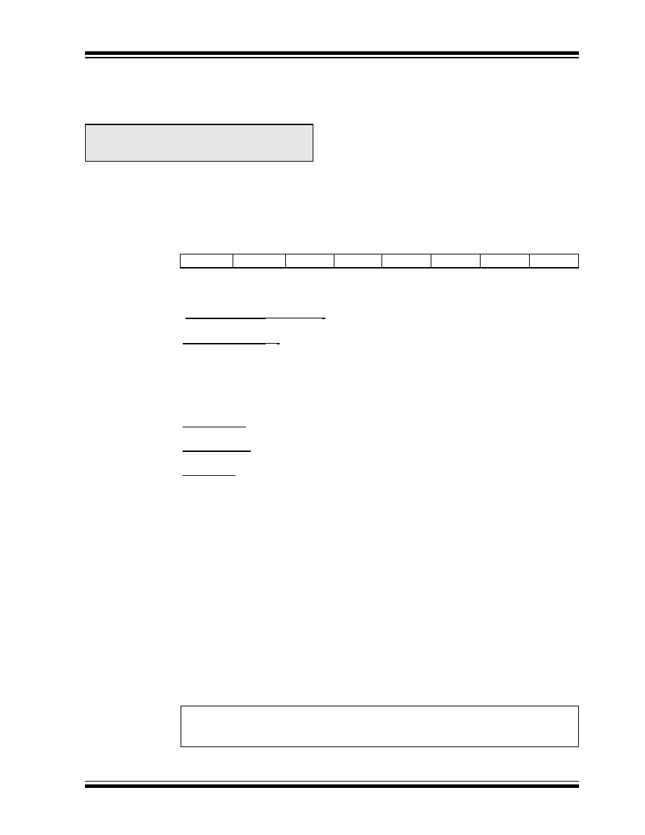
2002 Microchip Technology Inc.
Preliminary
DS41159B-page 129
PIC18FXX8
16.0
ENHANCED CAPTURE/
COMPARE/PWM (ECCP)
MODULE
This module contains a 16-bit register which can oper-
ate as a 16-bit Capture register, a 16-bit Compare
register, or a PWM Master/Slave Duty Cycle register.
The operation of the ECCP module differs from the
CCP (discussed in detail in Section 15.0) with the addi-
tion of an enhanced PWM module, which allows for up
to 4 output channels and user selectable polarity.
These features are discussed in detail in Section 16.5.
The module can also be programmed for automatic
shutdown in response to various analog or digital
events.
The control register for ECCP1 is shown in
Register 16-1.
REGISTER 16-1:
ECCP1CON REGISTER
Note:
The ECCP (Enhanced Capture/Compare/
PWM) module is only available on
PIC18F448 and PIC18F458 devices.
R/W-0
R/W-0
R/W-0
R/W-0
R/W-0
R/W-0
R/W-0
R/W-0
EPWM1M1 EPWM1M0
EDC1B1
EDC1B0
ECCP1M3 ECCP1M2 ECCP1M1 ECCP1M0
bit 7
bit 0
bit 7-6
EPWM1M<1:0>: PWM Output Configuration bits
If ECCP1M<3:2> =
00, 01, 10
:
xx
= P1A assigned as Capture/Compare input; P1B, P1C, P1D assigned as port pins
If ECCP1M<3:2> =
11
:
00
= Single output; P1A modulated; P1B, P1C, P1D assigned as port pins
01
= Full-bridge output forward; P1D modulated; P1A active; P1B, P1C inactive
10
= Half-bridge output; P1A, P1B modulated with deadband control; P1C, P1D assigned as
port pins
11
= Full-bridge output reverse; P1B modulated; P1C active; P1A, P1D inactive
bit 5-4
EDC1B<1:0>: PWM Duty Cycle Least Significant bits
Capture mode:
Unused
Compare mode:
Unused
PWM mode:
These bits are the two LSbs of the PWM duty cycle. The eight MSbs are found in ECCPR1L.
bit 3-0
ECCP1M<3:0>: ECCP1 Mode Select bits
0000
= Capture/Compare/PWM off (resets ECCP module)
0001
= Unused (reserved)
0010
= Compare mode, toggle output on match (ECCP1IF bit is set)
0011
= Unused (reserved)
0100
= Capture mode, every falling edge
0101
= Capture mode, every rising edge
0110
= Capture mode, every 4th rising edge
0111
= Capture mode, every 16th rising edge
1000
= Compare mode, set output on match (ECCP1IF bit is set)
1001
= Compare mode, clear output on match (ECCP1IF bit is set)
1010
= Compare mode, ECCP1 pin is unaffected (ECCP1IF bit is set)
1011
= Compare mode, trigger special event (ECCP1IF bit is set; ECCP resets TMR1or TMR3,
and starts an A/D conversion, if the A/D module is enabled)
1100
= PWM mode; P1A, P1C active high; P1B, P1D active high
1101
= PWM mode; P1A, P1C active high; P1B, P1D active low
1110
= PWM mode; P1A, P1C active low; P1B, P1D active high
1111
= PWM mode; P1A, P1C active low; P1B, P1D active low
Legend:
R = Readable bit
W = Writable bit
U = Unimplemented bit, read as `0'
- n = Value at POR
'1' = Bit is set
'0' = Bit is cleared
x = Bit is unknown
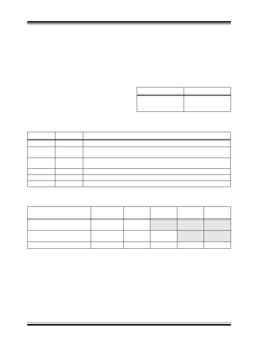
PIC18FXX8
DS41159B-page 130
Preliminary
2002 Microchip Technology Inc.
16.1
ECCP1 Module
Enhanced Capture/Compare/PWM Register1 (ECCPR1)
is comprised of two 8-bit registers: ECCPR1L (low
byte) and ECCPR1H (high byte). The ECCP1CON reg-
ister controls the operation of ECCP1; the additional
registers, ECCPAS and ECCP1DEL, control enhanced
PWM specific features. All registers are readable and
writable.
Table 16-1 shows the timer resources for the ECCP
module modes. Table 16-2 describes the interactions
of the ECCP module with the standard CCP module.
In PWM mode, the ECCP module can have up to four
available outputs, depending on which Operating mode
is selected. These outputs are multiplexed with PORTD
and the Parallel Slave Port. Both the Operating mode
and the output pin assignments are configured by setting
PWM Output Configuration bits EPWM1M1:EPWM1M0
(ECCP1CON<7:6>). The specific pin assignments for
the various Output modes are shown in Table 16-3.
TABLE 16-1:
ECCP1 MODE - TIMER
RESOURCE
TABLE 16-2:
INTERACTION OF CCP1 AND ECCP1 MODULES
TABLE 16-3:
PIN ASSIGNMENTS FOR VARIOUS ECCP MODES
ECCP1 Mode
Timer Resource
Capture
Compare
PWM
Timer1 or Timer3
Timer1 or Timer3
Timer2
ECCP1 Mode
CCP1 Mode
Interaction
Capture
Capture
TMR1 or TMR3 time-base. Time-base can be different for each CCP.
Capture
Compare
The compare could be configured for the special event trigger, which clears either
TMR1 or TMR3, depending upon which time-base is used.
Compare
Compare
The compare(s) could be configured for the special event trigger, which clears TMR1
or TMR3 depending upon which time-base is used.
PWM
PWM
The PWMs will have the same frequency and update rate (TMR2 interrupt).
PWM
Capture
None
PWM
Compare
None
ECCP Mode
(1)
ECCP1CON
Configuration
RD4
RD5
RD6
RD7
Conventional CCP Compatible
00xx11xx
ECCP1
RD<5>,
PSP<5>
RD<6>,
PSP<6>
RD<7>,
PSP<7>
Dual Output PWM
(2)
10xx11xx
P1A
P1B
RD<6>,
PSP<6>
RD<7>,
PSP<7>
Quad Output PWM
(2)
x1xx11xx
P1A
P1B
P1C
P1D
Legend:
x
= Don't care. Shaded cells indicate pin assignments not used by ECCP in a given mode.
Note 1: In all cases, the appropriate TRISD bits must be cleared to make the corresponding pin an output.
2: In these modes, the PSP I/O control for PORTD is overridden by P1B, P1C and P1D.
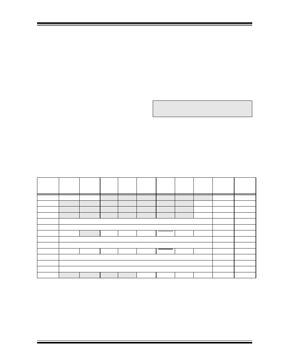
2002 Microchip Technology Inc.
Preliminary
DS41159B-page 131
PIC18FXX8
16.2
Capture Mode
The Capture Mode of the ECCP module is virtually
identical in operation to that of the standard CCP mod-
ule, as discussed in Section 15.1. The differences are
in the registers and port pins involved:
� The 16-bit Capture register is ECCPR1 (ECCPR1H
and ECCPR1L);
� The capture event is selected by control bits
ECCP1M3:ECCP1M0 (ECCP1CON<3:0>);
� The interrupt bits are ECCP1IE (PIE2<0>) and
ECCP1IF (PIR2<0>); and
� The capture input pin is RD4, and its corresponding
direction control bit is TRISD<4>.
Other operational details, including timer selection, out-
put pin configuration and software interrupts, are
exactly the same as the standard CCP module.
16.2.1
CAN MESSAGE TIME-STAMP
The special capture event for the reception of CAN
messages (Section 15.2.5) is not available with the
ECCP module.
16.3
Compare Mode
The Compare Mode of the ECCP module is virtually
identical in operation to that of the standard CCP mod-
ule, as discussed in Section 15.2. The differences are
in the registers and port pins, as described in
Section 16.2. All other details are exactly the same.
16.3.1
SPECIAL EVENT TRIGGER
Except as noted below, the special event trigger output
of ECCP1 functions identically to that of the standard
CCP module. It may be used to start an A/D conversion
if the A/D module is enabled.
TABLE 16-4:
REGISTERS ASSOCIATED WITH ENHANCED CAPTURE, COMPARE, TIMER1 AND
TIMER3
Note:
The special Event trigger from the ECCP1
module will not set the Timer1 or Timer3
interrupt flag bits.
Name
Bit 7
Bit 6
Bit 5
Bit 4
Bit 3
Bit 2
Bit 1
Bit 0
Value on
POR, BOR
Value on
all other
RESETS
INTCON
GIE/GIEH
PEIE/GIEL
TMR0IE
INT0IE
RBIE
TMR0IF
INT0IF
RBIF
0000 000x 0000 000u
PIR2
--
CMIF
--
EEIF
BCLIF
LVDIF
TMR3IF
ECCP1IF
-0-0 0000 -0-0 0000
PIE2
--
CMIE
--
EEIE
BCLIE
LVDIE
TMR3IE
ECCP1IE
-0-0 0000 -0-0 0000
IPR2
--
CMIP
--
EEIP
BCLIP
LVDIP
TMR3IP
ECCP1IP
-0-0 1111 -1-1 1111
TMR1L
Holding Register for the Least Significant Byte of the 16-bit TMR1 Register
xxxx xxxx uuuu uuuu
TMR1H
Holding Register for the Most Significant Byte of the 16-bit TMR1 Register
xxxx xxxx uuuu uuuu
T1CON
RD16
--
T1CKPS1 T1CKPS0 T1OSCEN
T1SYNC
TMR1CS
TMR1ON
0-00 0000 u-uu uuuu
TMR3L
Holding Register for the Least Significant Byte of the 16-bit TMR3 Register
xxxx xxxx uuuu uuuu
TMR3H
Holding Register for the Most Significant Byte of the 16-bit TMR3 Register
xxxx xxxx uuuu uuuu
T3CON
RD16
T3ECCP1 T3CKPS1 T3CKPS0
T3CCP1
T3SYNC
TMR3CS
TMR3ON
0000 0000 uuuu uuuu
TRISD
PORTD Data Direction Register
1111 1111 1111 1111
ECCPR1L
Capture/Compare/PWM Register1 (LSB)
xxxx xxxx uuuu uuuu
ECCPR1H
Capture/Compare/PWM Register1 (MSB)
xxxx xxxx uuuu uuuu
ECCP1CON EPWM1M1 EPWM1M0 EDC1B1
EDC1B0
ECCP1M3 ECCP1M2 ECCP1M1 ECCP1M0
0000 0000 0000 0000
Legend:
x
= unknown,
u
= unchanged,
-
= unimplemented, read as '0'. Shaded cells are not used by the ECCP module and Timer1.
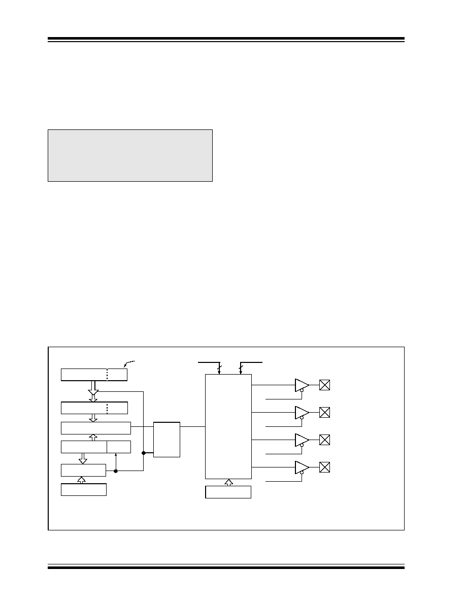
PIC18FXX8
DS41159B-page 132
Preliminary
2002 Microchip Technology Inc.
16.4
Standard PWM Mode
When configured in Single Output mode, the ECCP
module functions identically to the standard CCP mod-
ule in PWM mode, as described in Section 15.4. The
differences in registers and ports are as described in
Section 16.2; in addition, the two Least Significant bits
of the 10-bit PWM duty cycle value are represented by
ECCP1CON<5:4>.
16.5
Enhanced PWM Mode
The Enhanced PWM mode provides additional PWM
output options for a broader range of control applica-
tions. The module is an upwardly compatible version of
the standard CCP module and is modified to provide up
to four outputs, designated P1A through P1D. Users
are also able to select the polarity of the signal (either
active high or active low). The module's Output mode
and polarity are configured by setting the
EPWM1M1:EPWM1M0 and ECCP1M3:ECCP1M0 bits
of the ECCP1CON register (ECCP1CON<7:6> and
ECCP1CON<3:0>, respectively).
Figure 16-1 shows a simplified block diagram of PWM
operation. All control registers are double-buffered and
are loaded at the beginning of a new PWM cycle (the
period boundary when the assigned timer resets), in
order to prevent glitches on any of the outputs. The
exception is the PWM delay register ECCP1DEL,
which is loaded at either the duty cycle boundary or the
boundary period (whichever comes first). Because of
the buffering, the module waits until the assigned timer
resets, instead of starting immediately. This means that
enhanced PWM waveforms do not exactly match the
standard PWM waveforms, but are instead offset by
one full instruction cycle (4 T
OSC
).
As before, the user must manually configure the appro-
priate TRISD bits for output.
16.5.1
PWM OUTPUT CONFIGURATIONS
The EPWM1M<1:0> bits in the ECCP1CON register
allow one of four configurations:
� Single Output
� Half-Bridge Output
� Full-Bridge Output, Forward mode
� Full-Bridge Output, Reverse mode
The Single Output mode is the Standard PWM mode
discussed in Section 15.4. The Half-Bridge and Full-
Bridge Output modes are covered in detail in the
sections that follow.
The general relationship of the outputs in all
configurations is summarized in Figure 16-2.
FIGURE 16-1:
SIMPLIFIED BLOCK DIAGRAM OF THE ENHANCED PWM MODULE
Note:
When setting up single output PWM opera-
tions, users are free to use either of the pro-
cesses described in Section 15.4.3 or
Section 16.5.8. The latter is more generic,
but will work for either single or multi-output
PWM.
ECCPR1L
ECCPR1H (Slave)
Comparator
TMR2
Comparator
PR2
(Note 1)
R
Q
S
Duty Cycle Registers
ECCP1CON<5:4>
Clear Timer,
set ECCP1 pin and
latch D.C.
Note:
The 8-bit TMR2 register is concatenated with the 2-bit internal Q clock, or 2 bits of the prescaler to create the 10-bit time-base.
TRISD<4>
RD4/PSP4/ECCP1/P1A
TRISD<5>
RD5/PSP5/P1B
TRISD<6>
RD6/PSP6/P1C
TRISD<7>
RD7/PSP7/P1D
Output
Controller
EPWM1M1<1:0>
2
ECCP1M<3:0>
4
ECCP1DEL
ECCP1/P1A
P1B
P1C
P1D
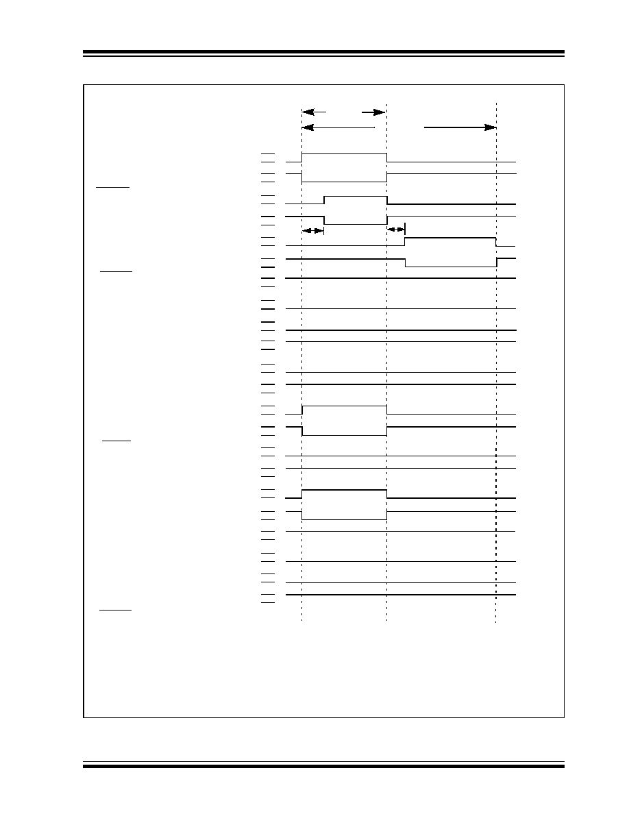
2002 Microchip Technology Inc.
Preliminary
DS41159B-page 133
PIC18FXX8
FIGURE 16-2:
PWM OUTPUT RELATIONSHIPS
0
PERIOD
00
10
01
11
Delay
Delay
SIGNAL
PR2+1
ECCP1CON
<7:6>
P1A Modulated, Active High
P1A Modulated, Active Low
P1A Modulated, Active High
P1A Modulated, Active Low
P1B Modulated, Active High
P1B Modulated, Active Low
P1A Active, Active High
P1A Active, Active Low
P1B Inactive, Active High
P1B Inactive, Active Low
P1C Inactive, Active High
P1C Inactive, Active Low
P1D Modulated, Active High
P1D Modulated, Active Low
P1A Inactive, Active High
P1A Inactive, Active Low
P1B Modulated, Active High
P1B Modulated, Active Low
P1C Active, Active High
P1C Active, Active Low
P1D Inactive, Active High
P1D Inactive, Active Low
Relationships:
� Period = 4 * T
OSC
* (PR2 + 1) * (TMR2 prescale value)
� Duty Cycle = T
OSC
* (CCPR1L<7:0>:CCP1CON<5:4>) * (TMR2 prescale value)
� Delay = 4 * T
OSC
* ECCP1DEL
DUTY
CYCLE
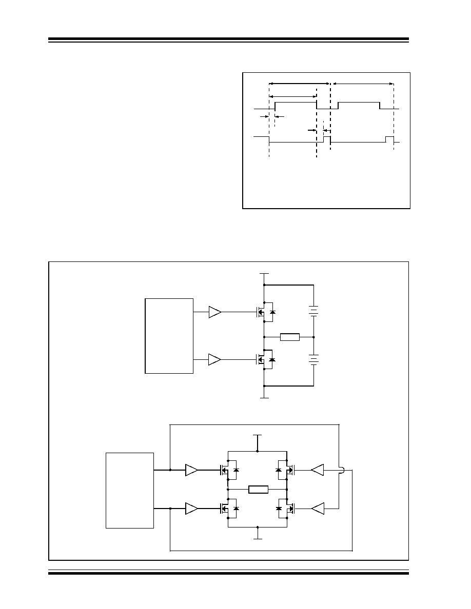
PIC18FXX8
DS41159B-page 134
Preliminary
2002 Microchip Technology Inc.
16.5.2
HALF-BRIDGE MODE
In the Half-Bridge Output mode, two pins are used as
outputs to drive push-pull loads. The RD4/PSP4/
ECCP1/P1A pin has the PWM output signal, while the
RD5/PSP5/P1B pin has the complementary PWM out-
put signal (Figure 16-3). This mode can be used for
half-bridge applications, as shown in Figure 16-4, or for
full-bridge applications, where four power switches are
being modulated with two PWM signals.
In Half-Bridge Output mode, the programmable dead-
band delay can be used to prevent shoot-through
current in bridge power devices. The value of register
ECCP1DEL dictates the number of clock cycles before
the output is driven active. If the value is greater than
the duty cycle, the corresponding output remains inac-
tive during the entire cycle. See Section 16.5.4 for
more details of the deadband delay operations.
Since the P1A and P1B outputs are multiplexed with
the PORTD<4> and PORTD<5> data latches, the
TRISD<4> and TRISD<5> bits must be cleared to
configure P1A and P1B as outputs.
FIGURE 16-3:
HALF-BRIDGE PWM
OUTPUT
FIGURE 16-4:
EXAMPLES OF HALF-BRIDGE OUTPUT MODE APPLICATIONS
Period
Duty Cycle
td
td
(1)
P1A
(2)
P1B
(2)
td = Deadband Delay
Period
(1)
(1)
Note
1: At this time, the TMR2 register is equal to the
PR2 register.
2: Output signals are shown as asserted high.
PIC18F448/458
P1A
P1B
FET
Driver
FET
Driver
V+
V-
Load
+ -
+
V
-
+
V
-
FET
Driver
FET
Driver
V+
V-
Load
+ -
FET
Driver
FET
Driver
PIC18F448/458
P1A
P1B
Standard Half-Bridge Circuit ("Push-Pull")
Half-Bridge Output Driving a Full-Bridge Circuit
2002 Microchip Technology Inc.
Preliminary
DS41159B-page 135
PIC18FXX8
16.5.3
FULL-BRIDGE MODE
In Full-Bridge Output mode, four pins are used as out-
puts; however, only two outputs are active at a time. In
the Forward mode, pin RD4/PSP4/ECCP1/P1A is con-
tinuously active, and pin RD7/PSP7/P1D is modulated.
In the Reverse mode, RD6/PSP6/P1C pin is continu-
ously active, and RD5/PSP5/P1B pin is modulated.
These are illustrated in Figure 16-5.
P1A, P1B, P1C and P1D outputs are multiplexed with
the PORTD<4:7> data latches. The TRISD<4:7> bits
must be cleared to make the P1A, P1B, P1C, and P1D
pins output.
FIGURE 16-5:
FULL-BRIDGE PWM OUTPUT
Period
Duty Cycle
P1A
(2)
P1B
(2)
P1C
(2)
P1D
(2)
FORWARD MODE
(1)
Period
Duty Cycle
P1A
(2)
P1C
(2)
P1D
(2)
P1B
(2)
REVERSE MODE
(1)
(1)
(1)
Note 1: At this time, the TMR2 register is equal to the PR2 register.
Note
2: Output signal is shown as asserted high.
PIC18FXX8
DS41159B-page 136
Preliminary
2002 Microchip Technology Inc.
FIGURE 16-6:
EXAMPLE OF FULL-BRIDGE APPLICATION
16.5.3.1
Direction Change in Full-Bridge
Mode
In the Full-Bridge Output mode, the EPWM1M1 bit in
the ECCP1CON register allows user to control the
Forward/Reverse direction. When the application firm-
ware changes this direction control bit, the ECCP1
module will assume the new direction on the next PWM
cycle. The current PWM cycle still continues, however,
the non-modulated outputs, P1A and P1C signals, will
transition to the new direction T
OSC
, 4 T
OSC
or 16 T
OSC
earlier (for T2CKRS<1:0> =
00
,
01
or
1x
, respectively),
before the end of the period. During this transition
cycle, the modulated outputs, P1B and P1D, will go to
the inactive state (Figure 16-7).
Note that in the Full-Bridge Output mode, the ECCP
module does not provide any deadband delay. In gen-
eral, since only one output is modulated at all times,
deadband delay is not required. However, there is a sit-
uation where a deadband delay might be required. This
situation occurs when all of the following conditions are
true:
1.
The direction of the PWM output changes when
the duty cycle of the output is at or near 100%.
2.
The turn off time of the power switch, including
the power device and driver circuit, is greater
than turn on time.
Figure 16-8 shows an example where the PWM direc-
tion changes from forward to reverse, at a near 100%
duty cycle. At time t1, the output P1A and P1D become
inactive, while output P1C becomes active. In this
example, since the turn off time of the power devices is
longer than the turn on time, a shoot-through current
flows through power devices QB and QD (see
Figure 16-6) for the duration of `t'. The same phenom-
enon will occur to power devices QA and QC for PWM
direction change from reverse to forward.
If changing PWM direction at high duty cycle is required
for an application, one of the following requirements
must be met:
1.
Avoid changing PWM output direction at or near
100% duty cycle.
2.
Use switch drivers that compensate the slow
turn off of the power devices. The total turn off
time (t
off
) of the power device and the driver
must be less than the turn on time (t
on
).
PIC18F448/458
P1D
P1B
FET
Driver
FET
Driver
V+
V-
Load
+
-
FET
Driver
FET
Driver
P1C
P1A
QD
QC
QA
QB
2002 Microchip Technology Inc.
Preliminary
DS41159B-page 137
PIC18FXX8
FIGURE 16-7:
PWM DIRECTION CHANGE
FIGURE 16-8:
PWM DIRECTION CHANGE AT NEAR 100% DUTY CYCLE
DC
PERIOD
SIGNAL
Note
1:
The direction bit in the ECCP1 Control Register (ECCP1CON.EPWM1M1) is written any time during the PWM
cycle.
2: The P1A and P1C signals switch at intervals of T
OSC
, 4 T
OSC
or 16 T
OSC
, depending on the Timer2 prescaler value
earlier when changing direction. The modulated P1B and P1D signals are inactive at this time.
(1)
PERIOD
(2)
P1A (Active High)
P1B (Active High)
P1C (Active High)
P1D (Active High)
FORWARD PERIOD
REVERSE PERIOD
(PWM)
P1A
(PWM)
t
on
t
off
t = t
off
� t
on
P1B
P1C
P1D
External Switch D
Potential
Shoot-Through
Current
Note
1: All signals are shown as active high.
2: t
on
is the Turn-on Delay of power switch and driver.
3: t
off
is the Turn-off Delay of power switch and driver.
External Switch C
t1

PIC18FXX8
DS41159B-page 138
Preliminary
2002 Microchip Technology Inc.
16.5.4
PROGRAMMABLE DEADBAND
DELAY
In half-bridge or full-bridge applications, where all
power switches are modulated at the PWM frequency
at all times, the power switches normally require longer
time to turn off than to turn on. If both the upper and
lower power switches are switched at the same time
(one turned on, and the other turned off), both switches
will be on for a short period of time until one switch
completely turns off. During this time, a very high cur-
rent (shoot-through current) flows through both power
switches, shorting the bridge supply. To avoid this
potentially destructive shoot-through current from flow-
ing during switching, turning on the power switch is nor-
mally delayed to allow the other switch to completely
turn off.
In the Half-Bridge Output mode, a digitally program-
mable deadband delay is available to avoid shoot-
through current from destroying the bridge power
switches. The delay occurs at the signal transition from
the non-active state to the active state. See Figure 16-3
for illustration. The ECCP1DEL register (Register 16-2)
sets the amount of delay.
16.5.5
SYSTEM IMPLEMENTATION
When the ECCP module is used in the PWM mode, the
application hardware must use the proper external pull-
up and/or pull-down resistors on the PWM output pins.
When the microcontroller powers up, all of the I/O pins
are in the high-impedance state. The external pull-up
and pull-down resistors must keep the power switch
devices in the off state, until the microcontroller drives
the I/O pins with the proper signal levels, or activates
the PWM output(s).
16.5.6
START-UP CONSIDERATIONS
Prior to enabling the PWM outputs, the P1A, P1B, P1C
and P1D latches may not be in the proper states.
Enabling the TRISD bits for output at the same time
with the ECCP1 module may cause damage to the
power switch devices. The ECCP1 module must be
enabled in the proper Output mode with the TRISD bits
enabled as inputs. Once the ECCP1 completes a full
PWM cycle, the P1A, P1B, P1C and 1PD output
latches are properly initialized. At this time, the TRISD
bits can be enabled for outputs to start driving the
power switch devices. The completion of a full PWM
cycle is indicated by the TMR2IF bit going from a '
0
' to
a '
1
'.
16.5.7
OUTPUT POLARITY
CONFIGURATION
The ECCP1M<1:0> bits in the ECCP1CON register
allow user to choose the logic conventions (asserted
high/low) for each of the outputs.
The PWM output polarities must be selected before the
PWM outputs are enabled. Charging the polarity con-
figuration while the PWM outputs are active is not rec-
ommended, since it may result in unpredictable
operation.
REGISTER 16-2:
ECCP1DEL REGISTER
R/W-0
R/W-0
R/W-0
R/W-0
R/W-0
R/W-0
R/W-0
R/W-0
EPDC7
EPDC6
EPDC5
EPDC4
EPDC3
EPDC2
EPDC1
EPDC0
bit 7
bit 0
bit 7-0
EPDC<7:0>: PWM Delay Count for Half-Bridge Output Mode bits
Number of F
OSC
/4 (T
OSC
*
4) cycles between the P1A transition and the P1B transition
Legend:
R = Readable bit
W = Writable bit
U = Unimplemented bit, read as `0'
- n = Value at POR
'1' = Bit is set
'0' = Bit is cleared
x = Bit is unknown
2002 Microchip Technology Inc.
Preliminary
DS41159B-page 139
PIC18FXX8
16.5.8
SETUP FOR PWM OPERATION
The following steps should be taken when configuring
the ECCP1 module for PWM operation:
1.
Configure the PWM module:
a)
Disable the ECCP1/P1A, P1B, P1C and/or
P1D outputs by setting the respective TRISD
bits.
b)
Set the PWM period by loading the PR2
register.
c)
Set the PWM duty cycle by loading the
ECCPR1L register and ECCP1CON<5:4> bits.
d)
Configure the ECCP1 module for the desired
PWM operation, by loading the ECCP1CON
register with the appropriate value. With the
ECCP1M<3:0> bits, select the active high/low
levels for each PWM output. With the
EPWM1M<1:0> bits, select one of the
available Output modes.
e)
For Half-Bridge Output mode, set the dead-
band delay by loading the ECCP1DEL
register with the appropriate value.
2.
Configure and start TMR2:
a)
Clear the TMR2 interrupt flag bit by clearing
the TMR2IF bit in the PIR1 register.
b)
Set the TMR2 prescale value by loading the
T2CKPS bits (T2CON<1:0>).
c)
Enable Timer2 by setting the TMR2ON bit
(T2CON<2>) register.
3.
Enable PWM outputs after a new cycle has
started:
a)
Wait until TMR2 overflows (TMR2IF bit
becomes a '
1
'). The new PWM cycle begins
here.
b)
Enable the ECCP1/P1A, P1B, P1C and/or
P1D pin outputs by clearing the respective
TRISD bits.
TABLE 16-5:
REGISTERS ASSOCIATED WITH ENHANCED PWM AND TIMER2
Name
Bit 7
Bit 6
Bit 5
Bit 4
Bit 3
Bit 2
Bit 1
Bit 0
Value on
POR, BOR
Value on
all other
RESETS
INTCON
GIE/GIEH
PEIE/GIEL
TMR0IE
INT0IE
RBIE
TMR0IF
INT0IF
RBIF
0000 000x 0000 000u
RCON
IPEN
--
--
RI
TO
PD
POR
BOR
0--1 11qq 0--q qquu
IPR2
--
CMIP
--
EEIP
BCLIP
LVDIP
TMR3IP
ECCP1IP
-0-0 1111 -1-1 1111
PIR2
--
CMIF
--
EEIF
BCLIF
LVDIF
TMR3IF
ECCP1IF
-0-0 0000 -0-0 0000
PIE2
--
CMIE
--
EEIE
BCLIE
LVDIE
TMR3IE
ECCP1IE
-0-0 0000 -0-0 0000
TMR2
Timer2 Module Register
0000 0000 0000 0000
PR2
Timer2 Module Period Register
1111 1111 1111 1111
T2CON
--
TOUTPS3
TOUTPS2 TOUTPS1 TOUTPS0
TMR2ON T2CKPS1 T2CKPS0
-000 0000 -000 0000
TRISD
PORTD Data Direction Register
1111 1111 1111 1111
ECCPR1H
Enhanced Capture/Compare/PWM Register1 High Byte
xxxx xxxx uuuu uuuu
ECCPR1L
Enhanced Capture/Compare/PWM Register1 Low Byte
xxxx xxxx uuuu uuuu
ECCP1CON EPWM1M1 EPWM1M0
EDC1B1
EDC1B0
ECCP1M3 ECCP1M2 ECCP1M1 ECCP1M0
0000 0000 0000 0000
ECCPAS
ECCPASE
ECCPAS2
ECCPAS1 ECCPAS0
PSSAC1
PSSAC0
PSSBD1
PSSBD0
0000 0000 0000 0000
ECCP1DEL
EPDC7
EPDC6
EPDC5
EPDC4
EPDC3
EPDC2
EPDC1
EPDC0
0000 0000 uuuu uuuu
Legend:
x
= unknown,
u
= unchanged,
-
= unimplemented, read as '0'. Shaded cells are not used by the ECCP module.

PIC18FXX8
DS41159B-page 140
Preliminary
2002 Microchip Technology Inc.
16.6
Enhanced CCP Auto-Shutdown
When the ECCP is programmed for any of the PWM
modes, the output pins associated with its function may
be configured for Auto-Shutdown.
Auto-Shutdown allows the internal output of either of
the two comparator modules, or the external interrupt
0, to asynchronously disable the ECCP output pins.
Thus, an external analog or digital event can discon-
tinue an ECCP sequence. The comparator output(s) to
be used is selected by setting the proper mode bits in
the ECCPAS register. To use external interrupt INT0 as
a shutdown event, INT0IE must be set. To use either of
the comparator module outputs as a shutdown event,
corresponding comparators must be enabled. When a
shutdown occurs, the selected output values
(PSSACn, PSSBDn) are written to the ECCP port pins.
The internal shutdown signal is gated with the outputs
and will immediately and asynchronously disable the
outputs. If the internal shutdown is still in effect at the
time a new cycle begins, that entire cycle is
suppressed, thus eliminating narrow, glitchy pulses.
The ECCPASE bit is set by hardware upon a compara-
tor event and can only be cleared in software. The
ECCP outputs can be re-enabled only by clearing the
ECCPASE bit.
The Auto-Shutdown mode can be manually entered by
writing a `
1
' to the ECCPASE bit.
REGISTER 16-3:
ECCPAS: ENHANCED CAPTURE/COMPARE/PWM/AUTO-SHUTDOWN
CONTROL REGISTER
R/W-0
R/W-0
R/W-0
R/W-0
R/W-0
R/W-0
R/W-0
R/W-0
ECCPASE ECCPAS2 ECCPAS1 ECCPAS0
PSSAC1
PSSAC0
PSSBD1
PSSBD0
bit 7
bit 0
bit 7
ECCPASE: ECCP Auto-Shutdown Event Status bit
0
= ECCP outputs enabled, no shutdown event
1
= A shutdown event has occurred, must be reset in software to re-enable ECCP
bit 6-4
ECCPAS<2:0>: ECCP Auto-Shutdown bits
000
= No Auto-Shutdown enabled, comparators have no effect on ECCP
001
= Comparator 1 output will cause shutdown
010
= Comparator 2 output will cause shutdown
011
= Either Comparator 1 or 2 can cause shutdown
100
= INT0
101
= INT0 or Comparator 1 output
110
= INT0 or Comparator 2 output
111
= INT0 or Comparator 1 or Comparator 2 output
bit 3-2
PSSACn: Pin A and C Shutdown State Control bits
00
= Drive Pins A and C to `0'
01
= Drive Pins A and C to `1'
1x
= Pins A and C tri-state
bit 1-0
PSSBDn: Pin B and D Shutdown State Control bits
00
= Drive Pins B and D to `0'
01
= Drive Pins B and D to `1'
1x
= Pins B and D tri-state
Legend:
R = Readable bit
W = Writable bit
U = Unimplemented bit, read as `0'
- n = Value at POR
'1' = Bit is set
'0' = Bit is cleared
x = Bit is unknown
2002 Microchip Technology Inc.
Preliminary
DS41159B-page 141
PIC18FXX8
17.0
MASTER SYNCHRONOUS
SERIAL PORT (MSSP)
MODULE
17.1
Master SSP (MSSP) Module
Overview
The Master Synchronous Serial Port (MSSP) module is
a serial interface useful for communicating with other
peripheral or microcontroller devices. These peripheral
devices may be serial EEPROMs, shift registers, dis-
play drivers, A/D converters, etc. The MSSP module
can operate in one of two modes:
� Serial Peripheral Interface (SPI)
� Inter-Integrated Circuit (I
2
C)
- Full Master mode
- Slave mode (with general address call)
The I
2
C interface supports the following modes in
hardware:
� Master mode
� Multi-Master mode
� Slave mode
17.2
Control Registers
The MSSP module has three associated registers.
These include a status register (SSPSTAT) and two
control registers (SSPCON1 and SSPCON2). The use
of these registers and their individual configuration bits
differ significantly, depending on whether the MSSP
module is operated in SPI or I
2
C mode.
Additional details are provided under the individual
sections.
17.3
SPI Mode
The SPI mode allows 8 bits of data to be synchronously
transmitted and received simultaneously. All four modes
of SPI are supported. To accomplish communication,
typically three pins are used:
� Serial Data Out (SDO) - RC5/SDO
� Serial Data In (SDI) - RC4/SDI/SDA
� Serial Clock (SCK) - RC3/SCK/SCL
Additionally, a fourth pin may be used when in a Slave
mode of operation:
� Slave Select (SS) - RF7/SS
Figure 17-1 shows the block diagram of the MSSP
module when operating in SPI mode.
FIGURE 17-1:
MSSP BLOCK DIAGRAM
(SPI MODE)
( )
Read
Write
Internal
Data Bus
SSPSR reg
SSPM3:SSPM0
bit0
Shift
Clock
SS Control
Enable
Edge
Select
Clock Select
TMR2 Output
T
OSC
Prescaler
4, 16, 64
2
Edge
Select
2
4
Data to TX/RX in SSPSR
TRIS bit
2
SMP:CKE
RC5/SDO
SSPBUF reg
RC4/SDI/SDA
RF7/SS
RC3/SCK/
SCL

PIC18FXX8
DS41159B-page 142
Preliminary
2002 Microchip Technology Inc.
17.3.1
REGISTERS
The MSSP module has four registers for SPI mode
operation. These are:
� MSSP Control Register1 (SSPCON1)
� MSSP Status Register (SSPSTAT)
� Serial Receive/Transmit Buffer (SSPBUF)
� MSSP Shift Register (SSPSR) - Not directly
accessible
SSPCON1 and SSPSTAT are the control and status
registers in SPI mode operation. The SSPCON1 regis-
ter is readable and writable. The lower 6 bits of the
SSPSTAT are read only. The upper two bits of the
SSPSTAT are read/write.
SSPSR is the shift register used for shifting data in or
out. SSPBUF is the buffer register to which data bytes
are written to or read from.
In receive operations, SSPSR and SSPBUF together
create a double buffered receiver. When SSPSR
receives a complete byte, it is transferred to SSPBUF
and the SSPIF interrupt is set.
During transmission, the SSPBUF is not double buff-
ered. A write to SSPBUF will write to both SSPBUF and
SSPSR.
REGISTER 17-1:
SSPSTAT: MSSP STATUS REGISTER (SPI MODE)
R/W-0
R/W-0
R-0
R-0
R-0
R-0
R-0
R-0
SMP
CKE
D/A
P
S
R/W
UA
BF
bit 7
bit 0
bit 7
SMP: Sample bit
SPI Master mode:
1
= Input data sampled at end of data output time
0
= Input data sampled at middle of data output time
SPI Slave mode:
SMP must be cleared when SPI is used in Slave mode
bit 6
CKE: SPI Clock Edge Select
When CKP = 0:
1
= Data transmitted on rising edge of SCK
0
= Data transmitted on falling edge of SCK
When CKP = 1:
1
= Data transmitted on falling edge of SCK
0
= Data transmitted on rising edge of SCK
bit 5
D/A: Data/Address bit
Used in I
2
C mode only
bit 4
P: STOP bit
Used in I
2
C mode only. This bit is cleared when the MSSP module is disabled, SSPEN is
cleared.
bit 3
S: START bit
Used in I
2
C mode only
bit 2
R/W: Read/Write bit information
Used in I
2
C mode only
bit 1
UA: Update Address
Used in I
2
C mode only
bit 0
BF: Buffer Full Status bit (Receive mode only)
1
= Receive complete, SSPBUF is full
0
= Receive not complete, SSPBUF is empty
Legend:
R = Readable bit
W = Writable bit
U = Unimplemented bit, read as `0'
- n = Value at POR
'1' = Bit is set
'0' = Bit is cleared
x = Bit is unknown

2002 Microchip Technology Inc.
Preliminary
DS41159B-page 143
PIC18FXX8
REGISTER 17-2:
SSPCON1: MSSP CONTROL REGISTER1 (SPI MODE)
R/W-0
R/W-0
R/W-0
R/W-0
R/W-0
R/W-0
R/W-0
R/W-0
WCOL
SSPOV
SSPEN
CKP
SSPM3
SSPM2
SSPM1
SSPM0
bit 7
bit 0
bit 7
WCOL: Write Collision Detect bit (Transmit mode only)
1
= The SSPBUF register is written while it is still transmitting the previous word
(must be cleared in software)
0
= No collision
bit 6
SSPOV: Receive Overflow Indicator bit
SPI Slave mode:
1
= A new byte is received while the SSPBUF register is still holding the previous data. In case
of overflow, the data in SSPSR is lost. Overflow can only occur in Slave mode.The user
must read the SSPBUF, even if only transmitting data, to avoid setting overflow
(must be cleared in software).
0
= No overflow
Note:
In Master mode, the overflow bit is not set since each new reception (and
transmission) is initiated by writing to the SSPBUF register.
bit 5
SSPEN: Synchronous Serial Port Enable bit
1
= Enables serial port and configures SCK, SDO, SDI, and SS as serial port pins
0
= Disables serial port and configures these pins as I/O port pins
Note:
When enabled, these pins must be properly configured as input or output.
bit 4
CKP: Clock Polarity Select bit
1
= IDLE state for clock is a high level
0
= IDLE state for clock is a low level
bit 3-0
SSPM3:SSPM0: Synchronous Serial Port Mode Select bits
0101
= SPI Slave mode, clock = SCK pin, SS pin control disabled, SS can be used as I/O pin
0100
= SPI Slave mode, clock = SCK pin, SS pin control enabled
0011
= SPI Master mode, clock = TMR2 output/2
0010
= SPI Master mode, clock = F
OSC
/64
0001
= SPI Master mode, clock = F
OSC
/16
0000
= SPI Master mode, clock = F
OSC
/4
Note:
Bit combinations not specifically listed here are either reserved, or implemented in
I
2
C mode only.
Legend:
R = Readable bit
W = Writable bit
U = Unimplemented bit, read as `0'
- n = Value at POR
'1' = Bit is set
'0' = Bit is cleared
x = Bit is unknown

PIC18FXX8
DS41159B-page 144
Preliminary
2002 Microchip Technology Inc.
17.3.2
OPERATION
When initializing the SPI, several options need to be
specified. This is done by programming the appropriate
control bits (SSPCON1<5:0>) and SSPSTAT<7:6>.
These control bits allow the following to be specified:
� Master mode (SCK is the clock output)
� Slave mode (SCK is the clock input)
� Clock Polarity (IDLE state of SCK)
� Data input sample phase (middle or end of data
output time)
� Clock edge (output data on rising/falling edge of
SCK)
� Clock Rate (Master mode only)
� Slave Select mode (Slave mode only)
The MSSP consists of a transmit/receive Shift Register
(SSPSR) and a buffer register (SSPBUF). The SSPSR
shifts the data in and out of the device, MSb first. The
SSPBUF holds the data that was written to the SSPSR,
until the received data is ready. Once the 8 bits of data
have been received, that byte is moved to the SSPBUF
register. Then the buffer full detect bit, BF
(SSPSTAT<0>), and the interrupt flag bit, SSPIF, are
set. This double buffering of the received data
(SSPBUF) allows the next byte to start reception before
reading the data that was just received. Any write to the
SSPBUF register during transmission/reception of data
will be ignored, and the write collision detect bit, WCOL
(SSPCON1<7>), will be set. User software must clear
the WCOL bit so that it can be determined if the follow-
ing write(s) to the SSPBUF register completed
successfully.
When the application software is expecting to receive
valid data, the SSPBUF should be read before the next
byte of data to transfer is written to the SSPBUF. Buffer
full bit, BF (SSPSTAT<0>), indicates when SSPBUF
has been loaded with the received data (transmission
is complete). When the SSPBUF is read, the BF bit is
cleared. This data may be irrelevant if the SPI is only a
transmitter. Generally, the MSSP Interrupt is used to
determine when the transmission/reception has com-
pleted. The SSPBUF must be read and/or written. If the
interrupt method is not going to be used, then software
polling can be done to ensure that a write collision does
not occur. Example 17-1 shows the loading of the
SSPBUF (SSPSR) for data transmission.
The SSPSR is not directly readable or writable, and
can only be accessed by addressing the SSPBUF reg-
ister. Additionally, the MSSP status register (SSPSTAT)
indicates the various status conditions.
EXAMPLE 17-1:
LOADING THE SSPBUF (SSPSR) REGISTER
LOOP BTFSS SSPSTAT, BF ;Has data been received(transmit complete)?
BRA LOOP ;No
MOVF SSPBUF, W ;WREG reg = contents of SSPBUF
MOVWF RXDATA ;Save in user RAM, if data is meaningful
MOVF TXDATA, W ;W reg = contents of TXDATA
MOVWF SSPBUF ;New data to xmit
2002 Microchip Technology Inc.
Preliminary
DS41159B-page 145
PIC18FXX8
17.3.3
ENABLING SPI I/O
To enable the serial port, SSP Enable bit, SSPEN
(SSPCON1<5>), must be set. To reset or reconfigure
SPI mode, clear the SSPEN bit, re-initialize the
SSPCON registers, and then set the SSPEN bit. This
configures the SDI, SDO, SCK, and SS pins as serial
port pins. For the pins to behave as the serial port func-
tion, some must have their data direction bits (in the
TRIS register) appropriately programmed as follows:
� SDI is automatically controlled by the SPI module
� SDO must have TRISC<5> bit cleared
� SCK (Master mode) must have TRISC<3> bit
cleared
� SCK (Slave mode) must have TRISC<3> bit set
� SS must have TRISF<7> bit set
Any serial port function that is not desired may be over-
ridden by programming the corresponding data direc-
tion (TRIS) register to the opposite value.
17.3.4
TYPICAL CONNECTION
Figure 17-2 shows a typical connection between two
microcontrollers. The master controller (Processor 1)
initiates the data transfer by sending the SCK signal.
Data is shifted out of both shift registers on their pro-
grammed clock edge, and latched on the opposite
edge of the clock. Both processors should be pro-
grammed to the same Clock Polarity (CKP), then both
controllers would send and receive data at the same
time. Whether the data is meaningful (or dummy data)
depends on the application software. This leads to
three scenarios for data transmission:
� Master sends data
--
Slave sends dummy data
� Master sends data
--
Slave sends data
� Master sends dummy data
--
Slave sends data
FIGURE 17-2:
SPI MASTER/SLAVE CONNECTION
Serial Input Buffer
(SSPBUF)
Shift Register
(SSPSR)
MSb
LSb
SDO
SDI
PROCESSOR 1
SCK
SPI Master SSPM3:SSPM0 =
00xxb
Serial Input Buffer
(SSPBUF)
Shift Register
(SSPSR)
LSb
MSb
SDI
SDO
PROCESSOR 2
SCK
SPI Slave SSPM3:SSPM0 =
010xb
Serial Clock
PIC18FXX8
DS41159B-page 146
Preliminary
2002 Microchip Technology Inc.
17.3.5
MASTER MODE
The master can initiate the data transfer at any time
because it controls the SCK. The master determines
when the slave (Processor 2, Figure 17-2) is to broad-
cast data by the software protocol.
In Master mode, the data is transmitted/received as
soon as the SSPBUF register is written to. If the SPI is
only going to receive, the SDO output could be dis-
abled (programmed as an input). The SSPSR register
will continue to shift in the signal present on the SDI pin
at the programmed clock rate. As each byte is
received, it will be loaded into the SSPBUF register as
if a normal received byte (interrupts and status bits
appropriately set). This could be useful in receiver
applications as a "Line Activity Monitor" mode.
The clock polarity is selected by appropriately program-
ming the CKP bit (SSPCON1<4>). This then, would
give waveforms for SPI communication as shown in
Figure 17-3, Figure 17-5, and Figure 17-6, where the
MSB is transmitted first. In Master mode, the SPI clock
rate (bit rate) is user programmable to be one of the
following:
� F
OSC
/4 (or T
CY
)
� F
OSC
/16 (or 4 � T
CY
)
� F
OSC
/64 (or 16 � T
CY
)
� Timer2 output/2
This allows a maximum data rate (at 40 MHz) of
10.00 Mbps.
Figure 17-3 shows the waveforms for Master mode.
When the CKE bit is set, the SDO data is valid before
there is a clock edge on SCK. The change of the input
sample is shown based on the state of the SMP bit. The
time when the SSPBUF is loaded with the received
data is shown.
FIGURE 17-3:
SPI MODE WAVEFORM (MASTER MODE)
SCK
(CKP = 0
SCK
(CKP = 1
SCK
(CKP = 0
SCK
(CKP = 1
4 Clock
Modes
Input
Sample
Input
Sample
SDI
bit7
bit0
SDO
bit7
bit6
bit5
bit4
bit3
bit2
bit1
bit0
bit7
bit0
SDI
SSPIF
(SMP = 1)
(SMP = 0)
(SMP = 1)
CKE = 1)
CKE = 0)
CKE = 1)
CKE = 0)
(SMP = 0)
Write to
SSPBUF
SSPSR to
SSPBUF
SDO
bit7
bit6
bit5
bit4
bit3
bit2
bit1
bit0
(CKE = 0)
(CKE = 1)
Next Q4 cycle
after Q2
2002 Microchip Technology Inc.
Preliminary
DS41159B-page 147
PIC18FXX8
17.3.6
SLAVE MODE
In Slave mode, the data is transmitted and received as
the external clock pulses appear on SCK. When the
last bit is latched, the SSPIF interrupt flag bit is set.
While in Slave mode, the external clock is supplied by
the external clock source on the SCK pin. This external
clock must meet the minimum high and low times as
specified in the electrical specifications.
While in SLEEP mode, the slave can transmit/receive
data. When a byte is received, the device will wake-up
from SLEEP.
17.3.7
SLAVE SELECT
SYNCHRONIZATION
The SS pin allows a Synchronous Slave mode. The
SPI must be in Slave mode with SS pin control
enabled (SSPCON1<3:0> = 04h). The pin must not
be driven low for the SS pin to function as an input.
The Data Latch must be high. When the SS pin is
low, transmission and reception are enabled and
the SDO pin is driven. When the SS pin goes high,
the SDO pin is no longer driven, even if in the mid-
dle of a transmitted byte, and becomes a floating
output. External pull-up/pull-down resistors may be
desirable, depending on the application.
When the SPI module resets, the bit counter is forced
to 0. This can be done by either forcing the SS pin to a
high level or clearing the SSPEN bit.
To emulate two-wire communication, the SDO pin can
be connected to the SDI pin. When the SPI needs to
operate as a receiver, the SDO pin can be configured
as an input. This disables transmissions from the SDO.
The SDI can always be left as an input (SDI function),
since it cannot create a bus conflict.
FIGURE 17-4:
SLAVE SYNCHRONIZATION WAVEFORM
Note 1: When the SPI is in Slave mode with SS
pin control enabled (SSPCON<3:0> =
0100
), the SPI module will reset if the SS
pin is set to V
DD
.
2: If the SPI is used in Slave mode with CKE
set, then the SS pin control must be
enabled.
SCK
(CKP = 1
SCK
(CKP = 0
Input
Sample
SDI
bit7
SDO
bit7
bit6
bit7
SSPIF
Interrupt
(SMP = 0)
CKE = 0)
CKE = 0)
(SMP = 0)
Write to
SSPBUF
SSPSR to
SSPBUF
SS
Flag
bit0
bit7
bit0
Next Q4 cycle
after Q2
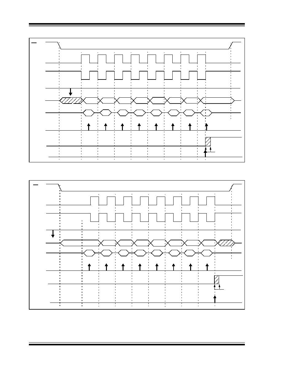
PIC18FXX8
DS41159B-page 148
Preliminary
2002 Microchip Technology Inc.
FIGURE 17-5:
SPI MODE WAVEFORM (SLAVE MODE WITH CKE = 0)
FIGURE 17-6:
SPI MODE WAVEFORM (SLAVE MODE WITH CKE = 1)
SCK
(CKP = 1
SCK
(CKP = 0
Input
Sample
SDI
bit7
bit0
SDO
bit7
bit6
bit5
bit4
bit3
bit2
bit1
bit0
SSPIF
Interrupt
(SMP = 0)
CKE = 0)
CKE = 0)
(SMP = 0)
Write to
SSPBUF
SSPSR to
SSPBUF
SS
Flag
Optional
Next Q4 cycle
after Q2
SCK
(CKP = 1
SCK
(CKP = 0
Input
Sample
SDI
bit7
bit0
SDO
bit7
bit6
bit5
bit4
bit3
bit2
bit1
bit0
SSPIF
Interrupt
(SMP = 0)
CKE = 1)
CKE = 1)
(SMP = 0)
Write to
SSPBUF
SSPSR to
SSPBUF
SS
Flag
Not Optional
Next Q4 cycle
after Q2
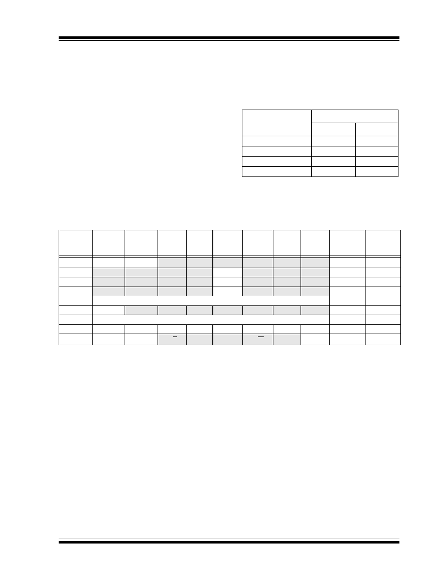
2002 Microchip Technology Inc.
Preliminary
DS41159B-page 149
PIC18FXX8
17.3.8
SLEEP OPERATION
In Master mode, all module clocks are halted and the
transmission/reception will remain in that state until the
device wakes from SLEEP. After the device returns to
normal mode, the module will continue to
transmit/receive data.
In Slave mode, the SPI transmit/receive shift register
operates asynchronously to the device. This allows the
device to be placed in SLEEP mode and data to be
shifted into the SPI transmit/receive shift register.
When all 8 bits have been received, the MSSP interrupt
flag bit will be set and if enabled, will wake the device
from SLEEP.
17.3.9
EFFECTS OF A RESET
A RESET disables the MSSP module and terminates
the current transfer.
17.3.10
BUS MODE COMPATIBILITY
Table 17-1 shows the compatibility between the
standard SPI modes and the states of the CKP and
CKE control bits.
TABLE 17-1:
SPI BUS MODES
There is also a SMP bit, which controls when the data
is sampled.
TABLE 17-2:
REGISTERS ASSOCIATED WITH SPI OPERATION
Standard SPI Mode
Terminology
Control Bits State
CKP
CKE
0, 0
0
1
0, 1
0
0
1, 0
1
1
1, 1
1
0
Name
Bit 7
Bit 6
Bit 5
Bit 4
Bit 3
Bit 2
Bit 1
Bit 0
Value on
POR, BOR
Value on
all other
RESETS
INTCON
GIE/GIEH
PEIE/GIEL
TMR0IE
INT0IE
RBIE
TMR0IF
INT0IF
RBIF
0000 0000 0000 0000
PIR1
PSPIF
ADIF
RCIF
TXIF
SSPIF
CCP1IF
TMR2IF
TMR1IF
0000 0000 0000 0000
PIE1
PSPIE
ADIE
RCIE
TXIE
SSPIE
CCP1IE
TMR2IE
TMR1IE
0000 0000 0000 0000
IPR1
PSPIP
ADIP
RCIP
TXIP
SSPIP
CCP1IP
TMR2IP
TMR1IP
0111 1111 0111 1111
TRISC
PORTC Data Direction Register
1111 1111 1111 1111
TRISF
TRISF7
TRISF6
TRISF5
TRISF4
TRISF3
TRISF2
TRISF1
TRISF0
1111 1111 uuuu uuuu
SSPBUF
Synchronous Serial Port Receive Buffer/Transmit Register
xxxx xxxx uuuu uuuu
SSPCON
WCOL
SSPOV
SSPEN
CKP
SSPM3
SSPM2
SSPM1
SSPM0
0000 0000 0000 0000
SSPSTAT
SMP
CKE
D/A
P
S
R/W
UA
BF
0000 0000 0000 0000
Legend:
x
= unknown,
u
= unchanged,
-
= unimplemented, read as '0'. Shaded cells are not used by the MSSP in SPI mode.
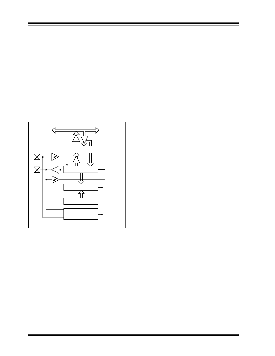
PIC18FXX8
DS41159B-page 150
Preliminary
2002 Microchip Technology Inc.
17.4
I
2
C Mode
The MSSP module in I
2
C mode fully implements all
master and slave functions (including general call sup-
port) and provides interrupts on START and STOP bits
in hardware to determine a free bus (multi-master func-
tion). The MSSP module implements the standard
mode specifications, as well as 7-bit and 10-bit
addressing.
Two pins are used for data transfer:
� Serial clock (SCL) - RC3/SCK/SCL
� Serial data (SDA) - RC4/SDI/SDA
The user must configure these pins as inputs or outputs
through the TRISC<4:3> bits.
FIGURE 17-7:
MSSP BLOCK DIAGRAM
(I
2
C MODE)
17.4.1
REGISTERS
The MSSP module has six registers for I
2
C operation.
These are:
� MSSP Control Register1 (SSPCON1)
� MSSP Control Register2 (SSPCON2)
� MSSP Status Register (SSPSTAT)
� Serial Receive/Transmit Buffer (SSPBUF)
� MSSP Shift Register (SSPSR) - Not directly
accessible
� MSSP Address Register (SSPADD)
SSPCON, SSPCON2 and SSPSTAT are the control
and status registers in I
2
C mode operation. The
SSPCON and SSPCON2 registers are readable and
writable. The lower 6 bits of the SSPSTAT are read
only. The upper two bits of the SSPSTAT are
read/write.
SSPSR is the shift register used for shifting data in or
out. SSPBUF is the buffer register to which data bytes
are written to or read from.
SSPADD register holds the slave device address
when the SSP is configured in I
2
C Slave mode. When
the SSP is configured in Master mode, the lower
seven bits of SSPADD act as the baud rate generator
reload value.
In receive operations, SSPSR and SSPBUF together,
create a double buffered receiver. When SSPSR
receives a complete byte, it is transferred to SSPBUF
and the SSPIF interrupt is set.
During transmission, the SSPBUF is not double buff-
ered. A write to SSPBUF will write to both SSPBUF and
SSPSR.
Read
Write
SSPSR reg
Match Detect
SSPADD reg
START and
STOP bit Detect
SSPBUF reg
Internal
Data Bus
Addr Match
Set, Reset
S, P bits
(SSPSTAT reg)
RC3/SCK/SCL
RC4/
Shift
Clock
MSb
SDI/
LSb
SDA

2002 Microchip Technology Inc.
Preliminary
DS41159B-page 151
PIC18FXX8
REGISTER 17-3:
SSPSTAT: MSSP STATUS REGISTER (I
2
C MODE)
R/W-0
R/W-0
R-0
R-0
R-0
R-0
R-0
R-0
SMP
CKE
D/A
P
S
R/W
UA
BF
bit 7
bit 0
bit 7
SMP: Slew Rate Control bit
In Master or Slave mode:
1
= Slew rate control disabled for Standard Speed mode (100 kHz and 1 MHz)
0
= Slew rate control enabled for High Speed mode (400 kHz)
bit 6
CKE: SMBus Select bit
In Master or Slave mode:
1
= Enable SMBus specific inputs
0
= Disable SMBus specific inputs
bit 5
D/A: Data/Address bit
In Master mode:
Reserved
In Slave mode:
1
= Indicates that the last byte received or transmitted was data
0
= Indicates that the last byte received or transmitted was address
bit 4
P: STOP bit
1
= Indicates that a STOP bit has been detected last
0
= STOP bit was not detected last
Note:
This bit is cleared on RESET and when SSPEN is cleared.
bit 3
S: START bit
1
= Indicates that a START bit has been detected last
0
= START bit was not detected last
Note:
This bit is cleared on RESET and when SSPEN is cleared.
bit 2
R/W: Read/Write bit Information (I
2
C mode only)
In Slave mode:
1
= Read
0
= Write
Note:
This bit holds the R/W bit information following the last address match. This bit is only
valid from the address match to the next START bit, STOP bit, or not ACK bit.
In Master mode:
1
= Transmit is in progress
0
= Transmit is not in progress
Note:
ORing this bit with SEN, RSEN, PEN, RCEN, or ACKEN will indicate if the MSSP is
in IDLE mode.
bit 1
UA: Update Address (10-bit Slave mode only)
1
= Indicates that the user needs to update the address in the SSPADD register
0
= Address does not need to be updated
bit 0
BF: Buffer Full Status bit
In Transmit mode:
1
= Receive complete, SSPBUF is full
0
= Receive not complete, SSPBUF is empty
In Receive mode:
1
= Data transmit in progress (does not include the ACK and STOP bits), SSPBUF is full
0
= Data transmit complete (does not include the ACK and STOP bits), SSPBUF is empty
Legend:
R = Readable bit
W = Writable bit
U = Unimplemented bit, read as `0'
- n = Value at POR
'1' = Bit is set
'0' = Bit is cleared
x = Bit is unknown

PIC18FXX8
DS41159B-page 152
Preliminary
2002 Microchip Technology Inc.
REGISTER 17-4:
SSPCON1: MSSP CONTROL REGISTER1 (I
2
C MODE)
R/W-0
R/W-0
R/W-0
R/W-0
R/W-0
R/W-0
R/W-0
R/W-0
WCOL
SSPOV
SSPEN
CKP
SSPM3
SSPM2
SSPM1
SSPM0
bit 7
bit 0
bit 7
WCOL: Write Collision Detect bit
In Master Transmit mode:
1
= A write to the SSPBUF register was attempted while the I
2
C conditions were not valid for
a transmission to be started (must be cleared in software)
0
= No collision
In Slave Transmit mode:
1
= The SSPBUF register is written while it is still transmitting the previous word (must be
cleared in software)
0
= No collision
In Receive mode (Master or Slave modes):
This is a "don't care" bit
bit 6
SSPOV: Receive Overflow Indicator bit
In Receive mode:
1
= A byte is received while the SSPBUF register is still holding the previous byte (must
be cleared in software)
0
= No overflow
In Transmit mode:
This is a "don't care" bit in Transmit mode
bit 5
SSPEN: Synchronous Serial Port Enable bit
1
= Enables the serial port and configures the SDA and SCL pins as the serial port pins
0
= Disables serial port and configures these pins as I/O port pins
Note:
When enabled, the SDA and SCL pins must be properly configured as input or output.
bit 4
CKP: SCK Release Control bit
In Slave mode:
1
= Release clock
0
= Holds clock low (clock stretch), used to ensure data setup time
In Master mode:
Unused in this mode
bit 3-0
SSPM3:SSPM0: Synchronous Serial Port Mode Select bits
1111
= I
2
C Slave mode, 10-bit address with START and STOP bit interrupts enabled
1110
= I
2
C Slave mode, 7-bit address with START and STOP bit interrupts enabled
1011
= I
2
C Firmware Controlled Master mode (Slave IDLE)
1000
= I
2
C Master mode, clock = F
OSC
/ (4 * (SSPADD+1))
0111
= I
2
C Slave mode, 10-bit address
0110
= I
2
C Slave mode, 7-bit address
Note:
Bit combinations not specifically listed here are either reserved, or implemented in
SPI mode only.
Legend:
R = Readable bit
W = Writable bit
U = Unimplemented bit, read as `0'
- n = Value at POR
'1' = Bit is set
'0' = Bit is cleared
x = Bit is unknown

2002 Microchip Technology Inc.
Preliminary
DS41159B-page 153
PIC18FXX8
REGISTER 17-5:
SSPCON2: MSSP CONTROL REGISTER 2 (I
2
C MODE)
R/W-0
R/W-0
R/W-0
R/W-0
R/W-0
R/W-0
R/W-0
R/W-0
GCEN
ACKSTAT
ACKDT
ACKEN
RCEN
PEN
RSEN
SEN
bit 7
bit 0
bit 7
GCEN: General Call Enable bit (Slave mode only)
1
= Enable interrupt when a general call address (0000h) is received in the SSPSR
0
= General call address disabled
bit 6
ACKSTAT: Acknowledge Status bit (Master Transmit mode only)
1
= Acknowledge was not received from slave
0
= Acknowledge was received from slave
bit 5
ACKDT: Acknowledge Data bit (Master Receive mode only)
1
= Not Acknowledge
0
= Acknowledge
Note:
Value that will be transmitted when the user initiates an Acknowledge sequence at
the end of a receive.
bit 4
ACKEN: Acknowledge Sequence Enable bit (Master Receive mode only)
1
= Initiate Acknowledge sequence on SDA and SCL pins, and transmit ACKDT data bit.
Automatically cleared by hardware.
0
= Acknowledge sequence IDLE
bit 3
RCEN: Receive Enable bit (Master Mode only)
1
= Enables Receive mode for I
2
C
0
= Receive IDLE
bit 2
PEN: STOP Condition Enable bit (Master mode only)
1
= Initiate STOP condition on SDA and SCL pins. Automatically cleared by hardware.
0
= STOP condition IDLE
bit 1
RSEN: Repeated START Condition Enabled bit (Master mode only)
1
= Initiate Repeated START condition on SDA and SCL pins.
Automatically cleared by hardware.
0
= Repeated START condition IDLE
bit 0
SEN: START Condition Enabled/Stretch Enabled bit
In Master mode:
1
= Initiate START condition on SDA and SCL pins. Automatically cleared by hardware.
0
= START condition IDLE
In Slave mode:
1
= Clock stretching is enabled for both Slave Transmit and Slave Receive (stretch enabled)
0
= Clock stretching is enabled for Slave Transmit only (Legacy mode)
Note:
For bits ACKEN, RCEN, PEN, RSEN, SEN: If the I
2
C module is not in the IDLE
mode, this bit may not be set (no spooling) and the SSPBUF may not be written (or
writes to the SSPBUF are disabled).
Legend:
R = Readable bit
W = Writable bit
U = Unimplemented bit, read as `0'
- n = Value at POR reset
'1' = Bit is set
'0' = Bit is cleared
x = Bit is unknown

PIC18FXX8
DS41159B-page 154
Preliminary
2002 Microchip Technology Inc.
17.4.2
OPERATION
The MSSP module functions are enabled by setting
MSSP Enable bit, SSPEN (SSPCON<5>).
The SSPCON1 register allows control of the I
2
C oper-
ation. Four mode selection bits (SSPCON<3:0>) allow
one of the following I
2
C modes to be selected:
� I
2
C Master mode, clock = OSC/4 (SSPADD +1)
� I
2
C Slave mode (7-bit address)
� I
2
C Slave mode (10-bit address)
� I
2
C Slave mode (7-bit address), with START and
STOP bit interrupts enabled
� I
2
C Slave mode (10-bit address), with START and
STOP bit interrupts enabled
� I
2
C Firmware controlled master operation, slave
is IDLE
Selection of any I
2
C mode, with the SSPEN bit set,
forces the SCL and SDA pins to be open drain, pro-
vided these pins are programmed to inputs by setting
the appropriate TRISC bits. To ensure proper operation
of the module, pull-up resistors must be provided
externally to the SCL and SDA pins.
17.4.3
SLAVE MODE
In Slave mode, the SCL and SDA pins must be config-
ured as inputs (TRISC<4:3> set). The MSSP module
will override the input state with the output data when
required (slave-transmitter).
The I
2
C Slave mode hardware will always generate an
interrupt on an address match. Through the mode
select bits, the user can also choose to interrupt on
START and STOP bits
When an address is matched or the data transfer after
an address match is received, the hardware automati-
cally will generate the Acknowledge (ACK) pulse and
load the SSPBUF register with the received value cur-
rently in the SSPSR register.
Any combination of the following conditions will cause
the MSSP module not to give this ACK pulse:
� The buffer full bit BF (SSPSTAT<0>) was set
before the transfer was received.
� The overflow bit SSPOV (SSPCON<6>) was set
before the transfer was received.
In this case, the SSPSR register value is not loaded
into the SSPBUF, but bit SSPIF (PIR1<3>) is set. The
BF bit is cleared by reading the SSPBUF register, while
bit SSPOV is cleared through software.
The SCL clock input must have a minimum high and
low for proper operation. The high and low times of the
I
2
C specification, as well as the requirement of the
MSSP module, are shown in timing parameter #100
and parameter #101.
17.4.3.1
Addressing
Once the MSSP module has been enabled, it waits for
a START condition to occur. Following the START con-
dition, the 8-bits are shifted into the SSPSR register. All
incoming bits are sampled with the rising edge of the
clock (SCL) line. The value of register SSPSR<7:1> is
compared to the value of the SSPADD register. The
address is compared on the falling edge of the eighth
clock (SCL) pulse. If the addresses match, and the BF
and SSPOV bits are clear, the following events occur:
1.
The SSPSR register value is loaded into the
SSPBUF register.
2.
The buffer full bit BF is set.
3.
An ACK pulse is generated.
4.
MSSP interrupt flag bit, SSPIF (PIR1<3>) is set
(interrupt is generated if enabled) on the falling
edge of the ninth SCL pulse.
In 10-bit Address mode, two address bytes need to be
received by the slave. The five Most Significant bits
(MSbs) of the first address byte specify if this is a 10-bit
address. Bit R/W (SSPSTAT<2>) must specify a write
so the slave device will receive the second address
byte. For a 10-bit address, the first byte would equal
`
11110 A9 A8 0
', where `
A9
' and `
A8
' are the two
MSbs of the address. The sequence of events for 10-bit
address is as follows, with steps 7 through 9 for the
slave-transmitter:
1.
Receive first (high) byte of Address (bits SSPIF,
BF and bit UA (SSPSTAT<1>) are set).
2.
Update the SSPADD register with second (low)
byte of Address (clears bit UA and releases the
SCL line).
3.
Read the SSPBUF register (clears bit BF) and
clear flag bit SSPIF.
4.
Receive second (low) byte of Address (bits
SSPIF, BF, and UA are set).
5.
Update the SSPADD register with the first (high)
byte of Address. If match releases SCL line, this
will clear bit UA.
6.
Read the SSPBUF register (clears bit BF) and
clear flag bit SSPIF.
7.
Receive Repeated START condition.
8.
Receive first (high) byte of Address (bits SSPIF
and BF are set).
9.
Read the SSPBUF register (clears bit BF) and
clear flag bit SSPIF.

2002 Microchip Technology Inc.
Preliminary
DS41159B-page 155
PIC18FXX8
17.4.3.2
Reception
When the R/W bit of the address byte is clear and an
address match occurs, the R/W bit of the SSPSTAT
register is cleared. The received address is loaded into
the SSPBUF register and the SDA line is held low
(ACK).
When the address byte overflow condition exists, then
the no Acknowledge (ACK) pulse is given. An overflow
condition is defined as either bit BF (SSPSTAT<0>) is
set, or bit SSPOV (SSPCON1<6>) is set.
An MSSP interrupt is generated for each data transfer
byte. Flag bit SSPIF (PIR1<3>) must be cleared in soft-
ware. The SSPSTAT register is used to determine the
status of the byte.
If SEN is enabled (SSPCON1<0>=1), RC3/SCK/SCL
will be held low (clock stretch) following each data
transfer. The clock must be released by setting bit CKP
(SSPCON<4>). See Section 17.4.4, Clock Stretching
for more detail.
17.4.3.3
Transmission
When the R/W bit of the incoming address byte is set
and an address match occurs, the R/W bit of the
SSPSTAT register is set. The received address is
loaded into the SSPBUF register. The ACK pulse will
be sent on the ninth bit and pin RC3/SCK/SCL is held
low, regardless of SEN (see Section 17.4.4, Clock
Stretching for more detail). By stretching the clock, the
master will be unable to assert another clock pulse until
the slave is done preparing the transmit data.The trans-
mit data must be loaded into the SSPBUF register,
which also loads the SSPSR register. Then pin
RC3/SCK/SCL should be enabled by setting bit CKP
(SSPCON1<4>). The eight data bits are shifted out on
the falling edge of the SCL input. This ensures that the
SDA signal is valid during the SCL high time
(Figure 17-9).
The ACK pulse from the master-receiver is latched on
the rising edge of the ninth SCL input pulse. If the SDA
line is high (not ACK), then the data transfer is com-
plete. In this case, when the ACK is latched by the
slave, the slave logic is reset (resets SSPSTAT regis-
ter) and the slave monitors for another occurrence of
the START bit. If the SDA line was low (ACK), the next
transmit data must be loaded into the SSPBUF register.
Again, pin RC3/SCK/SCL must be enabled by setting
bit CKP.
An MSSP interrupt is generated for each data transfer
byte. The SSPIF bit must be cleared in software and
the SSPSTAT register is used to determine the status
of the byte. The SSPIF bit is set on the falling edge of
the ninth clock pulse.
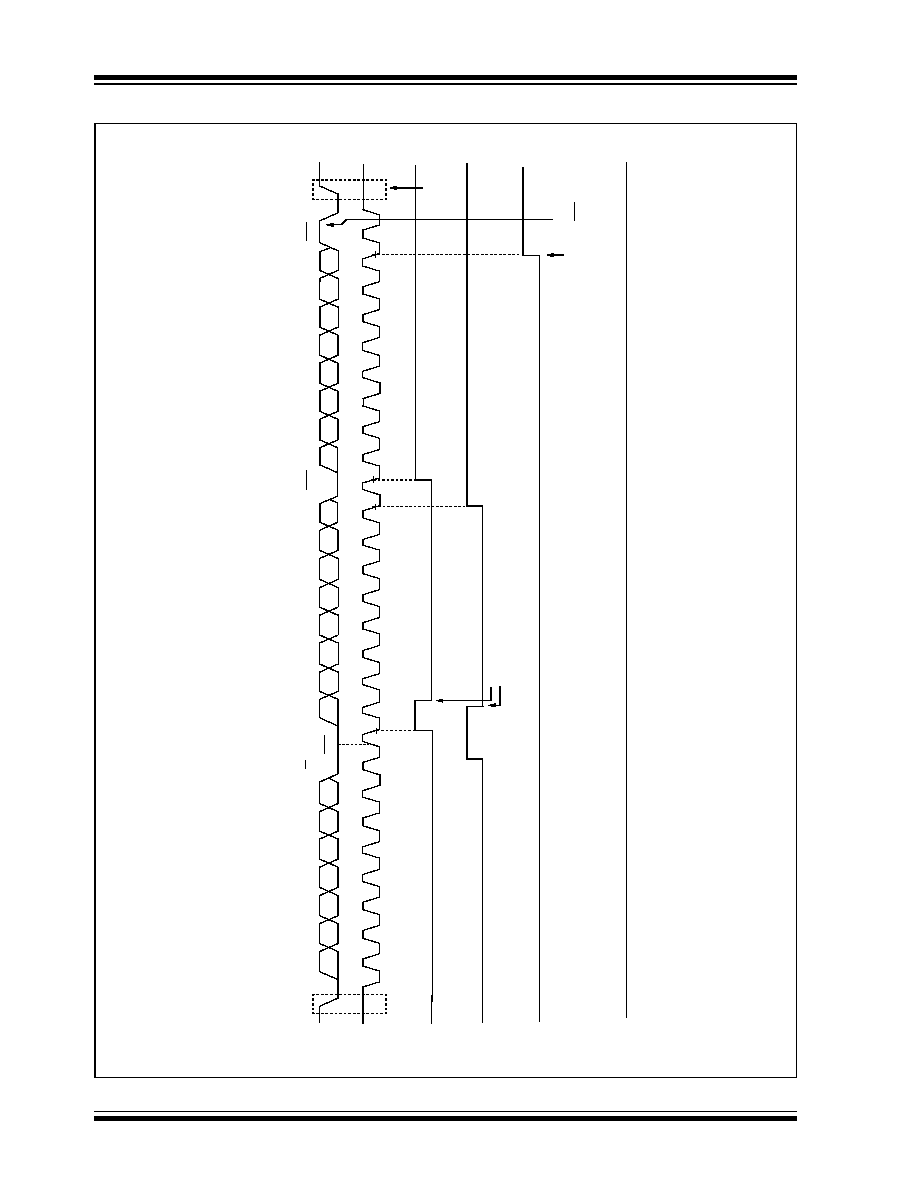
PIC18FXX8
DS41159B-page 156
Preliminary
2002 Microchip Technology Inc.
FIGURE 17-8:
I
2
C SLAVE MODE TIMING WITH SEN = 0 (RECEPTION, 7-BIT ADDRESS)
SDA
SCL
SSP
I
F
BF (
S
S
PST
A
T
<0
>)
S
SPO
V (
S
S
P
CO
N<6
>
)
S
1
2
3
4
56
7
8
9
1
23
4
5
6
7
89
1
2
3
4
5
7
8
9
P
A
7
A6
A
5
A
4
A
3
A
2
A
1
D7
D6
D5
D4
D3
D2
D1
D0
D7
D6
D5
D4
D3
D1
D0
ACK
Re
ce
ivin
g
Da
t
a
AC
K
Re
ce
ivin
g
Da
ta
R/W
=
0
AC
K
Re
ce
ivin
g
Ad
d
r
e
s
s
C
l
e
a
r
ed i
n
softw
ar
e
SSP
BUF
i
s
r
e
a
d
B
u
s M
a
ster
te
rmina
tes
tr
ansfer
S
S
P
OV
is set
be
cause S
S
P
B
U
F
i
s
still fu
l
l
.
A
C
K
i
s
not
sent.
D2
6
(P
IR
1<
3
>
)
CK
P
(C
K
P
does
not r
e
set to
`
0
'
w
hen S
E
N
=
0)
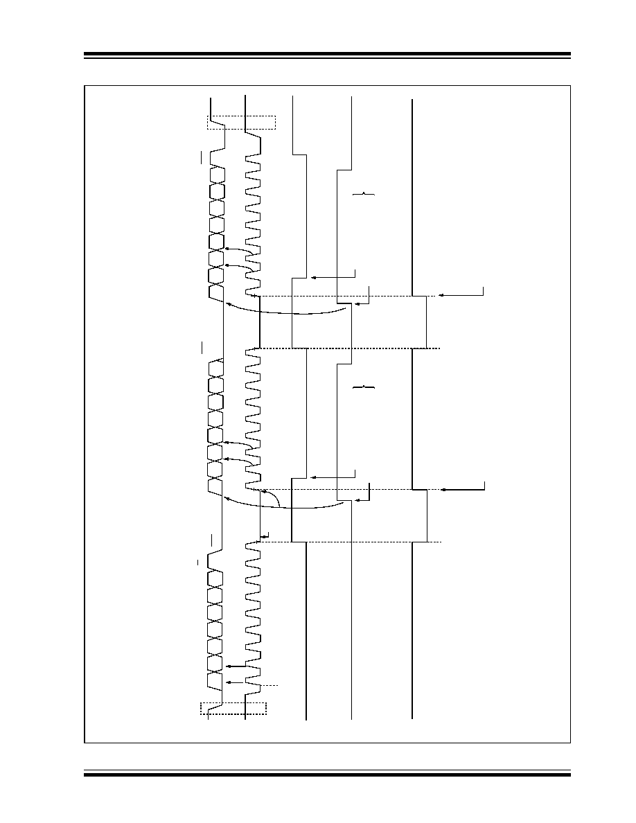
2002 Microchip Technology Inc.
Preliminary
DS41159B-page 157
PIC18FXX8
FIGURE 17-9:
I
2
C SLAVE MODE TIMING (TRANSMISSION, 7-BIT ADDRESS)
SD
A
SC
L
S
S
P
I
F
(P
I
R
1<
3>
)
B
F
(
SSP
ST
A
T
<
0
>)
A6
A5
A4
A3
A2
A1
D6
D5
D4
D3
D2
D1
D0
1
2
3
4
5
6
7
8
2
3
4
5
6
7
8
9
SSP
BU
F
i
s
w
r
it
t
e
n
in
s
o
f
t
w
a
r
e
C
l
eared i
n
sof
t
w
a
re
S
C
L hel
d l
o
w
wh
i
l
e
CP
U
responds to S
S
P
IF
F
r
o
m
SSPI
F
I
S
R
Data i
n
sam
p
led
S
AC
K
T
r
a
n
s
m
i
t
t
i
ng D
a
t
a
R/
W
=
1
AC
K
R
e
cei
v
i
ng A
ddres
s
A7
D
7
9
1
D6
D5
D4
D3
D2
D1
D0
2
3
4
5
6
7
8
9
S
S
P
B
U
F
is
w
r
it
te
n
in
s
o
ft
w
a
r
e
C
l
eared i
n
sof
t
w
a
re
Fr
o
m
SS
PI
F
I
S
R
T
r
ansmi
t
t
i
ng D
a
ta
D7
1
CK
P
P
ACK
C
K
P
is
s
e
t in
s
o
f
t
w
a
r
e
C
K
P
is
s
e
t in
s
o
f
t
w
a
r
e
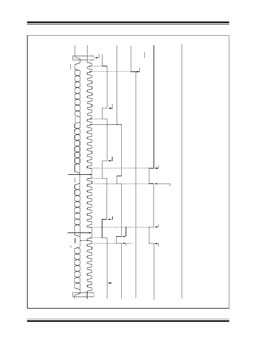
PIC18FXX8
DS41159B-page 158
Preliminary
2002 Microchip Technology Inc.
FIGURE 17-10:
I
2
C SLAVE MODE TIMING WITH SEN = 0 (RECEPTION, 10-BIT ADDRESS)
SDA
SCL
SS
PI
F
BF
(
S
SPS
T
A
T
<
0
>
)
S
1
2
3
4
56
7
8
9
1
2
3
4
5
6
7
89
1
2
3
4
5
7
8
9
P
1
1
1
1
0
A
9
A
8
A
7
A
6
A
5
A
4A
3A
2
A
1
A
0
D
7
D
6
D
5
D
4
D
3
D
1
D
0
Re
ce
i
v
e
Da
t
a
Byte
ACK
R/W
= 0
ACK
Re
ceive F
i
r
s
t B
y
te of A
d
d
r
ess
C
l
ea
r
e
d i
n
s
o
f
t
w
a
r
e
D2
6
(P
IR
1<
3>
)
C
l
ear
ed i
n
so
ftw
are
R
e
ce
i
v
e
S
e
cond B
y
te
of A
ddre
s
s
C
l
e
a
red
by har
dw
are
w
h
en S
S
P
A
D
D
i
s
update
d
w
i
th
l
o
w
byte
of add
ress
UA (
S
S
PST
A
T
<1
>)
Cl
o
ck is h
e
l
d
lo
w u
n
t
il
updat
e of S
S
P
A
D
D
has
ta
ken pl
a
c
e
UA
is
set indicat
i
n
g
tha
t
the S
S
P
A
D
D
need
s to be
upda
ted
U
A
i
s
set
i
n
di
cati
ng
that
S
S
P
A
D
D
need
s to be
u
pdate
d
C
l
e
a
r
ed
by har
dw
are
w
hen
S
S
P
A
D
D
i
s
upda
ted w
i
t
h
hi
gh
b
y
te of
addr
ess
S
SPB
UF
is wr
itte
n
wi
t
h
conten
ts o
f
S
S
P
S
R
D
u
mmy
read
of S
S
P
B
U
F
to clear
B
F
flag
AC
K
CKP
12
3
4
5
7
8
9
D7
D6
D5
D4
D3
D1
D0
Re
ce
ive
Da
ta
B
y
te
B
u
s M
a
ste
r
term
i
nates
tran
sfer
D2
6
ACK
Cle
a
r
e
d
in
so
f
t
wa
r
e
Cle
a
r
e
d
in
so
ft
w
a
r
e
SSP
O
V
(
S
SPCO
N
<
6
>
)
S
SPO
V
is
s
e
t
because
S
S
P
B
U
F
i
s
stil
l f
u
ll. AC
K
i
s
no
t sent.
(
C
K
P
do
es not
reset
to
`
0
'
w
hen
S
E
N
=
0)
Clo
ck is h
e
l
d
lo
w u
n
t
il
upda
te of
S
S
P
A
D
D
has
ta
k
e
n
pl
ac
e
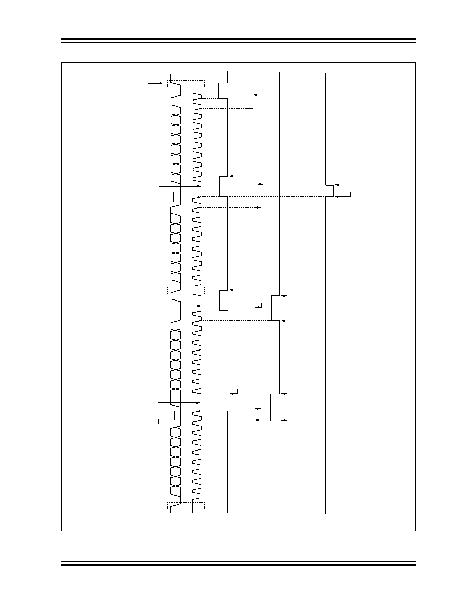
2002 Microchip Technology Inc.
Preliminary
DS41159B-page 159
PIC18FXX8
FIGURE 17-11:
I
2
C SLAVE MODE TIMING (TRANSMISSION, 10-BIT ADDRESS)
SDA
SCL
SSP
I
F
BF (
S
S
PST
A
T
<
0
>)
S
1
2
3
4
56
7
8
9
1
23
4
5
6
7
89
1
2
3
4
5
7
8
9
P
1
1
11
0
A
9
A
8
A
7
A
6
A
5
A
4
A
3
A
2
A
1
A
0
1
11
1
0
A
8
R/W=
1
AC
K
AC
K
R/W
=
0
ACK
R
e
ceive F
i
r
s
t B
y
te of
A
d
d
r
ess
Cle
a
r
e
d
in
so
f
t
wa
r
e
B
u
s M
a
ster
term
i
nates
tran
sfer
A9
6
(P
IR
1<
3>
)
R
e
ce
i
v
e
S
e
cond B
y
te
of A
ddre
s
s
C
l
ear
ed by
hard
w
are w
h
en
S
S
P
A
D
D
i
s
u
pdate
d
w
i
t
h l
o
w
byte
of ad
dress
UA (
S
S
PST
A
T
<1
>)
Clo
ck is h
e
ld
lo
w u
n
til
up
date o
f
S
S
P
A
D
D
ha
s
t
a
ken
pl
ace
UA
is se
t indicatin
g
that
the S
S
P
A
D
D
need
s to be
upda
ted
U
A
i
s
set
i
ndi
cati
ng
that
S
S
P
A
D
D
need
s to be
u
pdate
d
C
l
e
a
r
ed b
y
har
dw
are
w
hen
S
S
P
A
D
D
i
s
upda
ted w
i
t
h h
i
gh
b
y
te of a
ddre
ss.
SS
PBUF
is wr
i
t
te
n
with
cont
ent
s of S
S
P
S
R
D
u
mm
y re
ad of S
S
P
B
U
F
to cle
a
r B
F
f
l
a
g
R
e
cei
v
e F
i
rst B
y
te
of A
ddre
s
s
12
3
4
5
7
8
9
D
7
D6
D5
D4
D3
D
1
AC
K
D2
6
T
r
an
smitting D
a
ta
B
y
t
e
D0
D
u
mm
y re
ad of
S
S
P
B
U
F
to cle
a
r B
F
f
l
a
g
Sr
Cle
a
r
e
d
in
so
ftwa
r
e
W
r
it
e
o
f
SS
PBUF
in
itia
t
e
s tr
a
n
sm
it
C
l
ea
r
e
d i
n
s
o
f
t
w
a
r
e
Co
m
p
le
tio
n
o
f
cl
ear
s B
F
fl
ag
C
KP (
SSP
CO
N<4
>
)
CK
P
is set in
software
C
K
P
i
s
aut
omati
c
a
l
l
y
cl
e
a
red
i
n
har
dw
are
hol
di
ng
S
C
L
l
o
w
Clo
ck is h
e
l
d
lo
w u
n
t
il
upd
ate of
S
S
P
A
D
D
has
t
a
ken p
l
ace
da
ta
tran
smi
ssi
on
Clo
ck is h
e
ld
lo
w u
n
til
CK
P
is set to
`
1
'
B
F
f
l
a
g
is clear
th
i
r
d ad
dress s
equen
ce
at
the e
nd of t
h
e

PIC18FXX8
DS41159B-page 160
Preliminary
2002 Microchip Technology Inc.
17.4.4
CLOCK STRETCHING
Both 7- and 10-bit Slave modes implement automatic
clock stretching during a transmit sequence.
The SEN bit (SSPCON2<0>) allows clock stretching to
be enabled during receives. Setting SEN will cause
the SCL pin to be held low at the end of each data
receive sequence.
17.4.4.1
Clock Stretching for 7-bit Slave
Receive Mode (SEN = 1)
In 7-bit Slave Receive mode, on the falling edge of the
ninth clock at the end of the ACK sequence, if the BF
bit is set, the CKP bit in the SSPCON1 register is auto-
matically cleared, forcing the SCL output to be held
low. The CKP being cleared to `0' will assert the SCL
line low. The CKP bit must be set in the user's ISR
before reception is allowed to continue. By holding the
SCL line low, the user has time to service the ISR and
read the contents of the SSPBUF before the master
device can initiate another receive sequence. This will
prevent buffer overruns from occurring.
17.4.4.2
Clock Stretching for 10-bit Slave
Receive Mode (SEN = 1)
In 10-bit Slave Receive mode, during the address
sequence, clock stretching automatically takes place
but CKP is not cleared. During this time, if the UA bit is
set after the ninth clock, clock stretching is initiated.
The UA bit is set after receiving the upper byte of the
10-bit address, and following the receive of the second
byte of the 10-bit address with the R/W bit cleared to
`0'. The release of the clock line occurs upon updating
SSPADD. Clock stretching will occur on each data
receive sequence as described in 7-bit mode.
17.4.4.3
Clock Stretching for 7-bit Slave
Transmit Mode
7-bit Slave Transmit mode implements clock stretching
by clearing the CKP bit after the falling edge of the
ninth clock, if the BF bit is clear. This occurs, regard-
less of the state of the SEN bit.
The user's ISR must set the CKP bit before transmis-
sion is allowed to continue. By holding the SCL line
low, the user has time to service the ISR and load the
contents of the SSPBUF before the master device can
initiate another transmit sequence (see Figure 17-9).
17.4.4.4
Clock Stretching for 10-bit Slave
Transmit Mode
In 10-bit Slave Transmit mode, clock stretching is con-
trolled during the first two address sequences by the
state of the UA bit, just as it is in 10-bit Slave Receive
mode. The first two addresses are followed by a third
address sequence, which contains the high order bits
of the 10-bit address and the R/W bit set to `1'. After
the third address sequence is performed, the UA bit is
not set, the module is now configured in Transmit
mode, and clock stretching is controlled by the BF flag,
as in 7-bit Slave Transmit mode (see Figure 17-11).
Note 1: If the user reads the contents of the
SSPBUF before the falling edge of the
ninth clock, thus clearing the BF bit, the
CKP bit will not be cleared and clock
stretching will not occur.
2: The CKP bit can be set in software,
regardless of the state of the BF bit. The
user should be careful to clear the BF bit
in the ISR before the next receive
sequence, in order to prevent an overflow
condition.
Note:
If the user polls the UA bit and clears it by
updating the SSPADD register before the
falling edge of the ninth clock occurs, and if
the user hasn't cleared the BF bit by read-
ing the SSPBUF register before that time,
then the CKP bit will still NOT be asserted
low. Clock stretching on the basis of the
state of the BF bit only occurs during a data
sequence, not an address sequence.
Note 1: If the user loads the contents of SSPBUF,
setting the BF bit before the falling edge of
the ninth clock, the CKP bit will not be
cleared and clock stretching will not occur.
2: The CKP bit can be set in software,
regardless of the state of the BF bit.
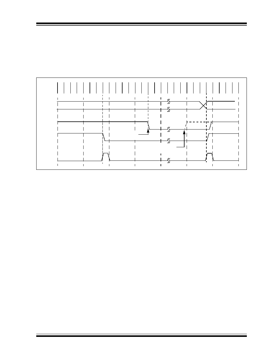
2002 Microchip Technology Inc.
Preliminary
DS41159B-page 161
PIC18FXX8
17.4.4.5
Clock Synchronization and
the CKP bit
If a user clears the CKP bit, the SCL output is forced to
`0'. Setting the CKP bit will not assert the SCL output
low until the SCL output is already sampled low. If the
user attempts to drive SCL low, the CKP bit will not
assert the SCL line until an external I
2
C master device
has already asserted the SCL line. The SCL output will
remain low until the CKP bit is set, and all other devices
on the I
2
C bus have de-asserted SCL. This ensures
that a write to the CKP bit will not violate the minimum
high time requirement for SCL (see Figure 17-12).
FIGURE 17-12:
CLOCK SYNCHRONIZATION TIMING
SDA
SCL
DX-1
DX
WR
Q1 Q2 Q3 Q4 Q1 Q2 Q3 Q4 Q1 Q2 Q3 Q4 Q1 Q2 Q3 Q4 Q1 Q2 Q3 Q4 Q1 Q2 Q3 Q4 Q1 Q2 Q3 Q4
SSPCON
CKP
Master device
de-asserts clock
Master device
asserts clock
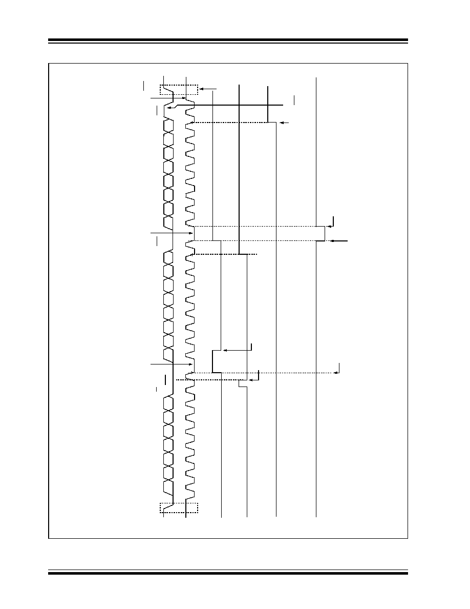
PIC18FXX8
DS41159B-page 162
Preliminary
2002 Microchip Technology Inc.
FIGURE 17-13:
I
2
C SLAVE MODE TIMING WITH SEN = 1 (RECEPTION, 7-BIT ADDRESS)
SDA
SCL
SS
PI
F
BF
(
S
SPS
T
A
T
<
0
>
)
SSP
O
V
(
S
SPCO
N
<
6
>
)
S
1
2
3
4
56
7
8
9
1
23
4
5
6
7
89
1
2
3
4
5
7
8
9
P
A
7
A6
A
5
A4
A
3
A2
A
1
D7
D6
D5
D4
D3
D
2
D1
D0
D7
D6
D5
D4
D3
D1
D0
ACK
Re
ce
ivin
g
Da
t
a
ACK
Re
ce
ivin
g
Da
t
a
R/W
= 0
ACK
R
e
cei
v
i
ng A
ddr
ess
Cle
a
r
e
d
in
so
f
t
wa
r
e
SSP
BUF
i
s
r
e
a
d
B
u
s M
a
st
er
ter
m
i
nate
s
tra
n
sfer
S
SPO
V
is
s
e
t
becau
se S
S
P
B
U
F
i
s
still fu
ll. ACK
is n
o
t sent
.
D2
6
(P
IR
1<
3>
)
CK
P
CK
P
wr
itte
n
to
`
1
'
in
If B
F
i
s
cleare
d
pr
ior to
the fa
l
lin
g
edg
e of t
he 9th
cl
ock,
CKP
will n
o
t b
e
r
e
se
t
to
`
0
'
and n
o
cl
ock
str
e
tch
i
n
g
will o
ccu
r
softwar
e
Clo
ck
i
s
h
e
l
d
lo
w u
n
til
CK
P
is set to
`
1
'
Clo
ck is n
o
t h
e
l
d
lo
w
be
cause b
u
f
f
er
ful
l
bi
t i
s
cl
ear
pr
i
o
r to
fal
l
i
ng ed
ge
of 9th
cl
ock
C
l
o
ck i
s
not
hel
d l
o
w
becau
se A
C
K
= 1
BF
i
s
se
t
a
fte
r
fa
llin
g
e
dge o
f
the 9
t
h cl
ock,
CK
P
is rese
t to
`
0
'
an
d
clock str
e
tch
i
ng
occu
r
s
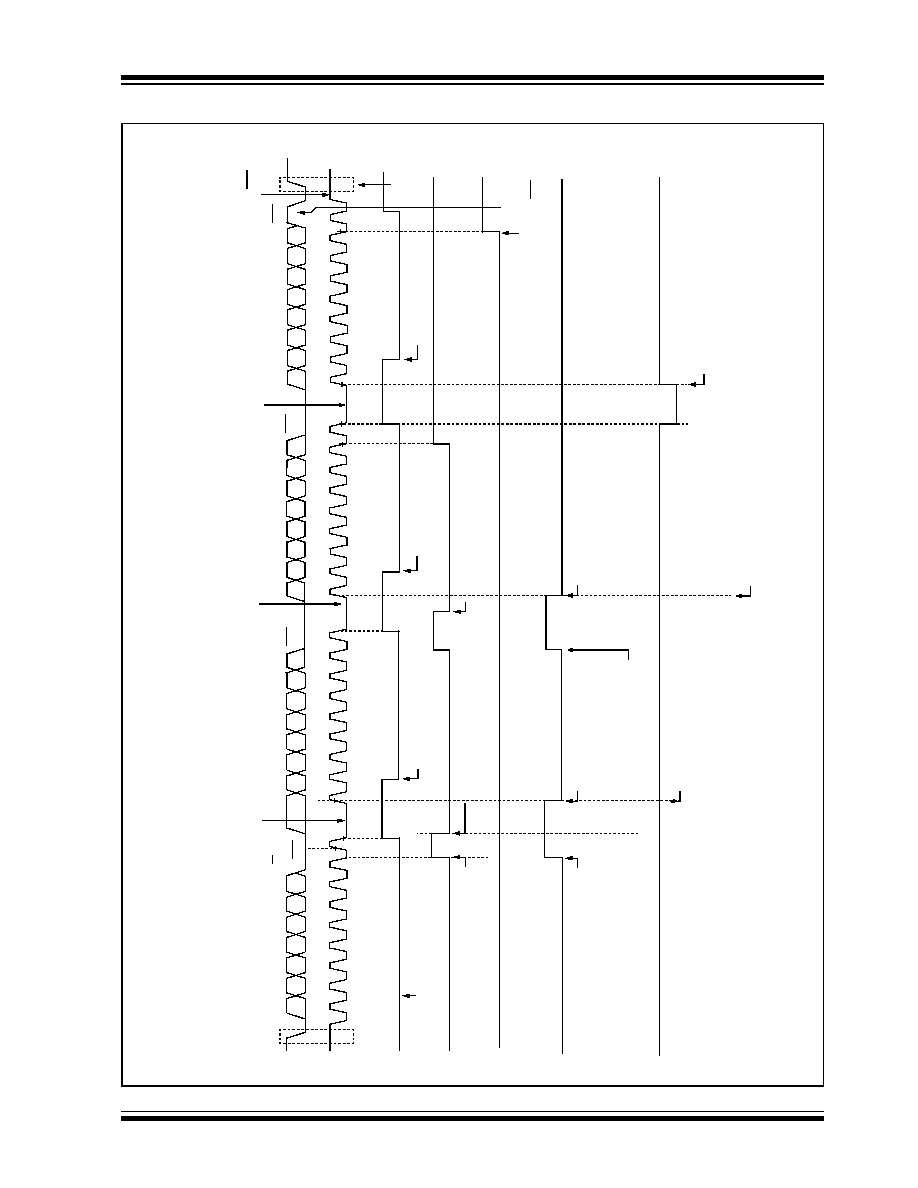
2002 Microchip Technology Inc.
Preliminary
DS41159B-page 163
PIC18FXX8
FIGURE 17-14:
I
2
C SLAVE MODE TIMING SEN = 1 (RECEPTION, 10-BIT ADDRESS)
SD
A
SC
L
S
SPI
F
B
F
(
S
S
PST
A
T
<0
>)
S
1
2
3
4
56
7
8
9
1
23
4
5
6
7
89
1
2
3
4
5
7
8
9
P
1
1
1
1
0
A
9A
8
A
7
A
6
A
5
A
4
A
3
A
2
A
1
A
0
D
7D
6D
5
D
4
D
3
D
1
D
0
Re
ce
ive
Da
t
a
B
y
te
AC
K
R/W
= 0
ACK
Receive F
i
rst B
y
te o
f
A
ddre
s
s
C
l
ea
r
e
d i
n
s
o
f
t
w
ar
e
D2
6
(P
IR
1<
3>
)
C
l
ea
r
e
d i
n
s
o
f
t
w
ar
e
R
e
cei
v
e S
e
co
nd B
y
te of
A
d
d
r
ess
C
l
e
a
r
ed
by har
dw
are
w
hen
S
S
P
A
D
D
i
s
upda
ted w
i
t
h
l
o
w
b
y
te of
addr
ess afte
r
falling
edge
UA
(
S
SPS
T
A
T
<
1
>
)
Clo
ck is h
e
ld
lo
w u
n
til
up
date o
f
S
S
P
A
D
D
ha
s
t
a
ken
pl
ace
U
A
i
s
set
i
n
di
cati
ng
that
th
e S
S
P
A
D
D
n
eeds to
be
u
pdate
d
UA
is se
t indicatin
g
that
S
S
P
A
D
D
nee
ds to b
e
upda
ted
C
l
ear
ed by h
a
rdw
a
re w
h
e
n
S
S
P
A
D
D
i
s
u
pdate
d
w
i
t
h hi
gh
byte
of ad
dress a
fter
fal
l
i
ng ed
ge
SSP
BUF is
wr
it
t
e
n
w
i
t
h
co
ntent
s o
f
S
S
P
S
R
D
u
mm
y read
of S
S
P
B
U
F
to clear
B
F
flag
AC
K
CK
P
12
3
4
5
7
8
9
D7
D6
D
5
D4
D3
D1
D0
Re
ce
ive
Da
t
a
Byte
B
u
s M
a
ster
term
i
nates
tran
sfer
D2
6
AC
K
C
l
e
a
r
ed i
n
softw
ar
e
C
l
ea
r
e
d i
n
s
o
f
t
w
a
r
e
SS
PO
V (
SSP
CO
N<6
>
)
CK
P
written
to
`
1
'
No
t
e
:
A
n
up
date
of th
e S
S
P
A
D
D
r
e
g
i
ste
r
b
e
fo
r
e
t
h
e
fa
llin
g
ed
ge of
the n
i
nth cl
ock
w
i
l
l
ha
ve no ef
fe
ct on U
A
, and
UA will
r
e
m
a
in
se
t.
No
t
e
:
A
n
up
date of the
S
S
P
A
D
D
re
g
i
s
t
er
be
f
o
r
e
t
h
e f
a
l
l
i
n
g
e
dge
of the
ninth
clock will
h
a
ve no
e
f
fect on U
A
, and
UA will r
e
m
a
in
se
t.
in softwar
e
Clo
ck is h
e
l
d
l
o
w u
n
t
il
upda
te of S
S
P
A
D
D
has
ta
k
e
n
pl
ac
e
of n
i
nth cl
ock.
o
f
ni
nth
cl
ock.
SS
PO
V is
s
e
t
be
cause S
S
P
B
U
F i
s
still fu
ll. ACK
i
s
not se
nt.
D
u
m
m
y r
ead of
S
S
P
B
U
F
to
cl
e
a
r B
F
flag
Clo
ck is h
e
ld
lo
w u
n
t
i
l
CK
P
is se
t to
`
1
'
Clo
ck is n
o
t
h
e
ld
lo
w
be
c
a
u
s
e A
C
K
= 1
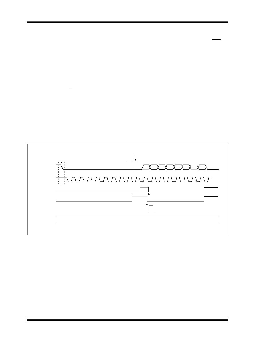
PIC18FXX8
DS41159B-page 164
Preliminary
2002 Microchip Technology Inc.
17.4.5
GENERAL CALL ADDRESS
SUPPORT
The addressing procedure for the I
2
C bus is such that
the first byte after the START condition usually deter-
mines which device will be the slave addressed by the
master. The exception is the general call address,
which can address all devices. When this address is
used, all devices should, in theory, respond with an
Acknowledge.
The general call address is one of eight addresses
reserved for specific purposes by the I
2
C protocol. It
consists of all 0's with R/W = 0.
The general call address is recognized when the Gen-
eral Call Enable bit (GCEN) is enabled (SSPCON2<7>
set). Following a START bit detect, 8-bits are shifted
into the SSPSR and the address is compared against
the SSPADD. It is also compared to the general call
address and fixed in hardware.
If the general call address matches, the SSPSR is
transferred to the SSPBUF, the BF flag bit is set (eighth
bit), and on the falling edge of the ninth bit (ACK bit),
the SSPIF interrupt flag bit is set.
When the interrupt is serviced, the source for the inter-
rupt can be checked by reading the contents of the
SSPBUF. The value can be used to determine if the
address was device specific or a general call address.
In 10-bit mode, the SSPADD is required to be updated
for the second half of the address to match, and the UA
bit is set (SSPSTAT<1>). If the general call address is
sampled when the GCEN bit is set, while the slave is
configured in 10-bit Address mode, then the second
half of the address is not necessary, the UA bit will not
be set, and the slave will begin receiving data after the
Acknowledge (Figure 17-15).
FIGURE 17-15:
SLAVE MODE GENERAL CALL ADDRESS SEQUENCE
(7 OR 10-BIT ADDRESS MODE)
SDA
SCL
S
SSPIF
BF (SSPSTAT<0>)
SSPOV (SSPCON1<6>)
Cleared in software
SSPBUF is read
R/W = 0
ACK
General Call Address
Address is compared to General Call Address
GCEN (SSPCON2<7>)
Receiving data
ACK
1
2
3
4
5
6
7
8
9
1
2
3
4
5
6
7
8
9
D7
D6
D5
D4
D3
D2
D1
D0
after ACK, set interrupt
'0'
'1'
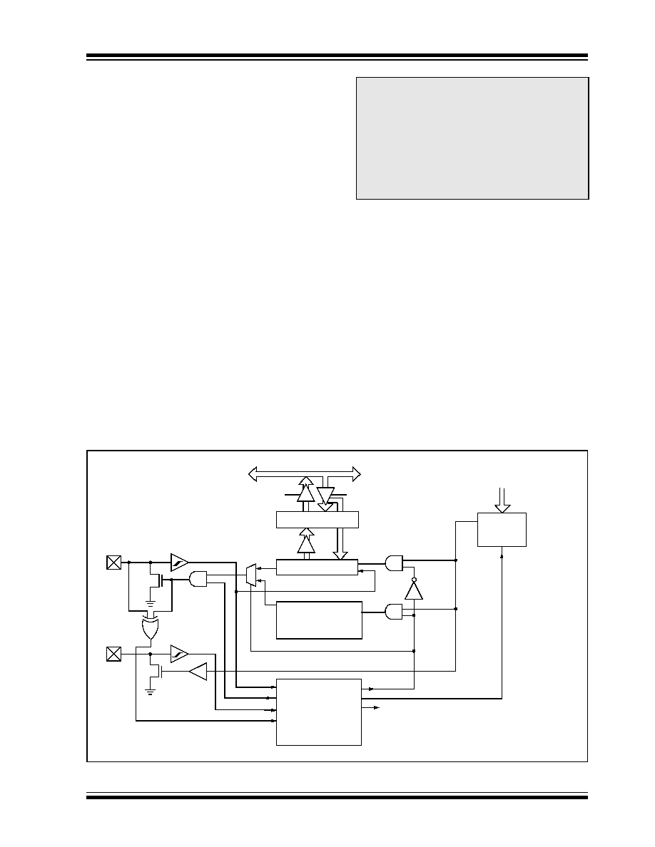
2002 Microchip Technology Inc.
Preliminary
DS41159B-page 165
PIC18FXX8
17.4.6
MASTER MODE
Master mode is enabled by setting and clearing the
appropriate SSPM bits in SSPCON1 and by setting the
SSPEN bit. In Master mode, the SCL and SDA lines
are manipulated by the MSSP hardware.
Master mode of operation is supported by interrupt
generation on the detection of the START and STOP
conditions. The STOP (P) and START (S) bits are
cleared from a RESET or when the MSSP module is
disabled. Control of the I
2
C bus may be taken when the
P bit is set or the bus is IDLE, with both the S and P bits
clear.
In Firmware Controlled Master mode, user code con-
ducts all I
2
C bus operations based on START and
STOP bit conditions.
Once Master mode is enabled, the user has six
options.
1.
Assert a START condition on SDA and SCL.
2.
Assert a Repeated START condition on SDA
and SCL.
3.
Write to the SSPBUF register initiating transmis-
sion of data/address.
4.
Configure the I
2
C port to receive data.
5.
Generate an Acknowledge condition at the end
of a received byte of data.
6.
Generate a STOP condition on SDA and SCL.
The following events will cause SSP interrupt flag bit,
SSPIF, to be set (SSP interrupt if enabled):
� START condition
� STOP condition
� Data transfer byte transmitted/received
� Acknowledge Transmit
� Repeated START
FIGURE 17-16:
MSSP BLOCK DIAGRAM (I
2
C MASTER MODE)
Note:
The MSSP Module, when configured in I
2
C
Master mode, does not allow queueing of
events. For instance, the user is not
allowed to initiate a START condition and
immediately write the SSPBUF register to
initiate transmission before the START
condition is complete. In this case, the
SSPBUF will not be written to and the
WCOL bit will be set, indicating that a write
to the SSPBUF did not occur.
Read
Write
SSPSR
START bit, STOP bit,
START bit Detect
SSPBUF
Internal
Data Bus
Set/Reset, S, P, WCOL (SSPSTAT)
Shift
Clock
MSb
LSb
SDA
Acknowledge
Generate
STOP bit Detect
Write Collision Detect
Clock Arbitration
State Counter for
end of XMIT/RCV
SCL
SCL in
Bus Collision
SDA in
Receive Enable
Cloc
k
Cnt
l
Clock
A
r
bit
r
at
e/
W
C
O
L
Det
e
ct
(hold
of
f
clock sour
ce)
SSPADD<6:0>
Baud
Set SSPIF, BCLIF
Reset ACKSTAT, PEN (SSPCON2)
Rate
Generator
SSPM3:SSPM0

PIC18FXX8
DS41159B-page 166
Preliminary
2002 Microchip Technology Inc.
17.4.6.1
I
2
C Master Mode Operation
The master device generates all of the serial clock
pulses and the START and STOP conditions. A trans-
fer is ended with a STOP condition or with a Repeated
START condition. Since the Repeated START condi-
tion is also the beginning of the next serial transfer, the
I
2
C bus will not be released.
In Master Transmitter mode, serial data is output
through SDA, while SCL outputs the serial clock. The
first byte transmitted contains the slave address of the
receiving device (7 bits) and the Read/Write (R/W) bit.
In this case, the R/W bit will be logic '0'. Serial data is
transmitted 8 bits at a time. After each byte is transmit-
ted, an Acknowledge bit is received. START and STOP
conditions are output to indicate the beginning and the
end of a serial transfer.
In Master Receive mode, the first byte transmitted con-
tains the slave address of the transmitting device
(7 bits) and the R/W bit. In this case, the R/W bit will be
logic '1'. Thus, the first byte transmitted is a 7-bit slave
address followed by a '1' to indicate receive bit. Serial
data is received via SDA, while SCL outputs the serial
clock. Serial data is received 8 bits at a time. After each
byte is received, an Acknowledge bit is transmitted.
START and STOP conditions indicate the beginning
and end of transmission.
The baud rate generator used for the SPI mode opera-
tion is used to set the SCL clock frequency for either
100 kHz, 400 kHz or 1 MHz I
2
C operation. See
Section 17.4.7, Baud Rate Generator for more details.
A typical transmit sequence would go as follows:
1.
The user generates a START condition by set-
ting the START enable bit, SEN
(SSPCON2<0>).
2.
SSPIF is set. The MSSP module will wait the
required start time before any other operation
takes place.
3.
The user loads the SSPBUF with the slave
address to transmit.
4.
Address is shifted out the SDA pin until all 8 bits
are transmitted.
5.
The MSSP module shifts in the ACK bit from the
slave device and writes its value into the
SSPCON2 register (SSPCON2<6>).
6.
The MSSP module generates an interrupt at the
end of the ninth clock cycle by setting the SSPIF
bit.
7.
The user loads the SSPBUF with eight bits of
data.
8.
Data is shifted out the SDA pin until all 8 bits are
transmitted.
9.
The MSSP Module shifts in the ACK bit from the
slave device and writes its value into the
SSPCON2 register (SSPCON2<6>).
10. The MSSP module generates an interrupt at the
end of the ninth clock cycle by setting the SSPIF
bit.
11. The user generates a STOP condition by setting
the STOP enable bit PEN (SSPCON2<2>).
12. Interrupt is generated once the STOP condition
is complete.
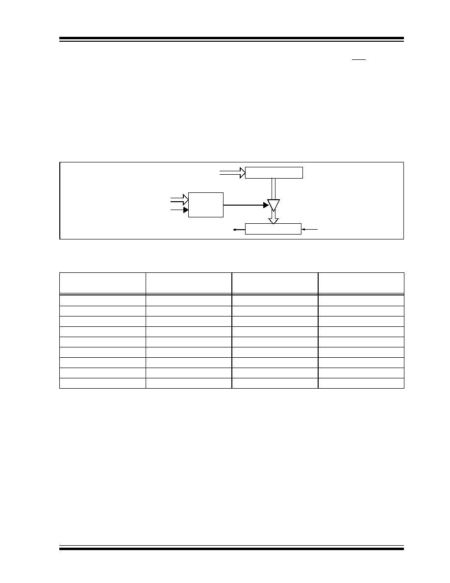
2002 Microchip Technology Inc.
Preliminary
DS41159B-page 167
PIC18FXX8
17.4.7
BAUD RATE GENERATOR
In I
2
C Master mode, the baud rate generator (BRG)
reload value is placed in the lower 7 bits of the
SSPADD register (Figure 17-17). When a write occurs
to SSPBUF, the baud rate generator will automatically
begin counting. The BRG counts down to 0 and stops
until another reload has taken place. The BRG count is
decremented twice per instruction cycle (T
CY
) on the
Q2 and Q4 clocks. In I
2
C Master mode, the BRG is
reloaded automatically.
Once the given operation is complete (i.e., transmis-
sion of the last data bit is followed by ACK), the internal
clock will automatically stop counting and the SCL pin
will remain in its last state.
Table 17-3 demonstrates clock rates based on
instruction cycles and the BRG value loaded into
SSPADD.
FIGURE 17-17:
BAUD RATE GENERATOR BLOCK DIAGRAM
TABLE 17-3:
I
2
C CLOCK RATE W/BRG
SSPM3:SSPM0
BRG Down Counter
CLKO
F
OSC
/4
SSPADD<6:0>
SSPM3:SSPM0
SCL
Reload
Control
Reload
F
CY
F
CY
*2
BRG Value
F
SCL
(2)
(2 Rollovers of BRG)
10 MHz
20 MHz
19h
400 kHz
(1)
10 MHz
20 MHz
20h
312.5 kHz
10 MHz
20 MHz
3Fh
100 kHz
4 MHz
8 MHz
0Ah
400 kHz
(1)
4 MHz
8 MHz
0Dh
308 kHz
4 MHz
8 MHz
28h
100 kHz
1 MHz
2 MHz
03h
333 kHz
(1)
1 MHz
2 MHz
0Ah
100kHz
1 MHz
2 MHz
00h
1 MHz
(1)
Note 1: The I
2
C interface does not conform to the 400 kHz I
2
C specification (which applies to rates greater than
100 kHz) in all details, but may be used with care where higher rates are required by the application.
2: Actual frequency will depend on bus conditions.
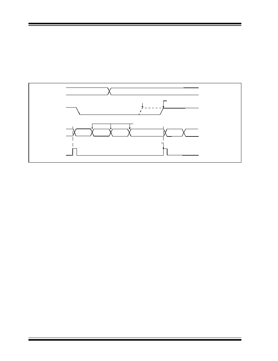
PIC18FXX8
DS41159B-page 168
Preliminary
2002 Microchip Technology Inc.
17.4.7.1
Clock Arbitration
Clock arbitration occurs when the master, during any
receive, transmit or Repeated START/STOP condition,
de-asserts the SCL pin (SCL allowed to float high).
When the SCL pin is allowed to float high, the baud rate
generator (BRG) is suspended from counting until the
SCL pin is actually sampled high. When the SCL pin is
sampled high, the baud rate generator is reloaded with
the contents of SSPADD<6:0> and begins counting.
This ensures that the SCL high time will always be at
least one BRG rollover count, in the event that the clock
is held low by an external device (Figure 17-18).
FIGURE 17-18:
BAUD RATE GENERATOR TIMING WITH CLOCK ARBITRATION
SDA
SCL
SCL de-asserted but slave holds
DX-1
DX
BRG
SCL is sampled high, reload takes
place and BRG starts its count.
03h
02h
01h
00h (hold off)
03h
02h
Reload
BRG
Value
SCL low (clock arbitration)
SCL allowed to transition high
BRG decrements on
Q2 and Q4 cycles
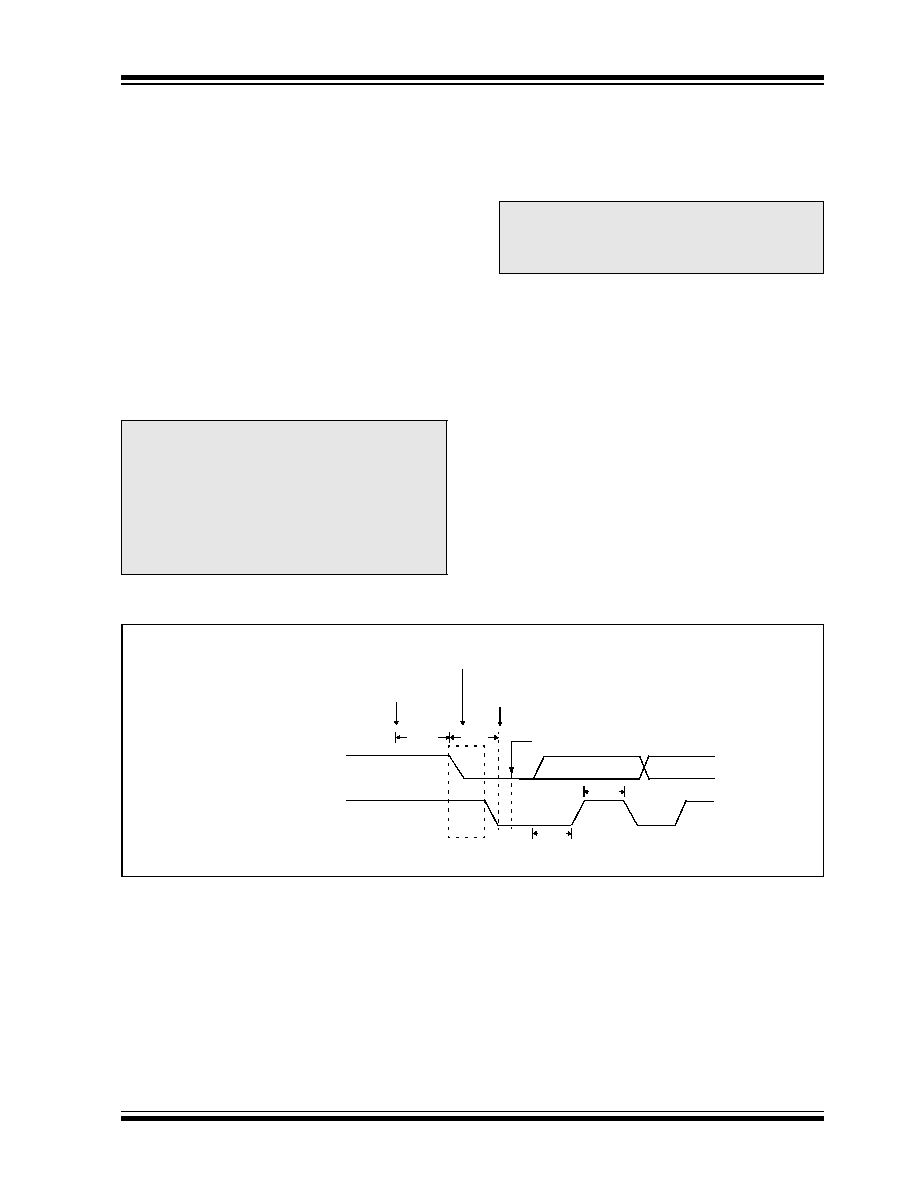
2002 Microchip Technology Inc.
Preliminary
DS41159B-page 169
PIC18FXX8
17.4.8
I
2
C MASTER MODE START
CONDITION TIMING
To initiate a START condition, the user sets the START
condition enable bit, SEN (SSPCON2<0>). If the SDA
and SCL pins are sampled high, the baud rate genera-
tor is reloaded with the contents of SSPADD<6:0> and
starts its count. If SCL and SDA are both sampled high
when the baud rate generator times out (T
BRG
), the
SDA pin is driven low. The action of the SDA being
driven low, while SCL is high, is the START condition
and causes the S bit (SSPSTAT<3>) to be set. Follow-
ing this, the baud rate generator is reloaded with the
contents of SSPADD<6:0> and resumes its count.
When the baud rate generator times out (T
BRG
), the
SEN bit (SSPCON2<0>) will be automatically cleared
by hardware, the baud rate generator is suspended,
leaving the SDA line held low and the START condition
is complete.
17.4.8.1
WCOL Status Flag
If the user writes the SSPBUF when a START
sequence is in progress, the WCOL is set and the con-
tents of the buffer are unchanged (the write doesn't
occur).
FIGURE 17-19:
FIRST START BIT TIMING
Note:
If, at the beginning of the START condition,
the SDA and SCL pins are already sam-
pled low, or if during the START condition
the SCL line is sampled low before the
SDA line is driven low, a bus collision
occurs, the Bus Collision Interrupt Flag,
BCLIF is set, the START condition is
aborted, and the I
2
C module is reset into its
IDLE state.
Note:
Because queueing of events is not
allowed, writing to the lower 5 bits of
SSPCON2 is disabled until the START
condition is complete.
SDA
SCL
S
T
BRG
1st bit
2nd bit
T
BRG
SDA = 1,
At completion of START bit,
SCL = 1
Write to SSPBUF occurs here
T
BRG
Hardware clears SEN bit
T
BRG
Write to SEN bit occurs here
Set S bit (SSPSTAT<3>)
and sets SSPIF bit
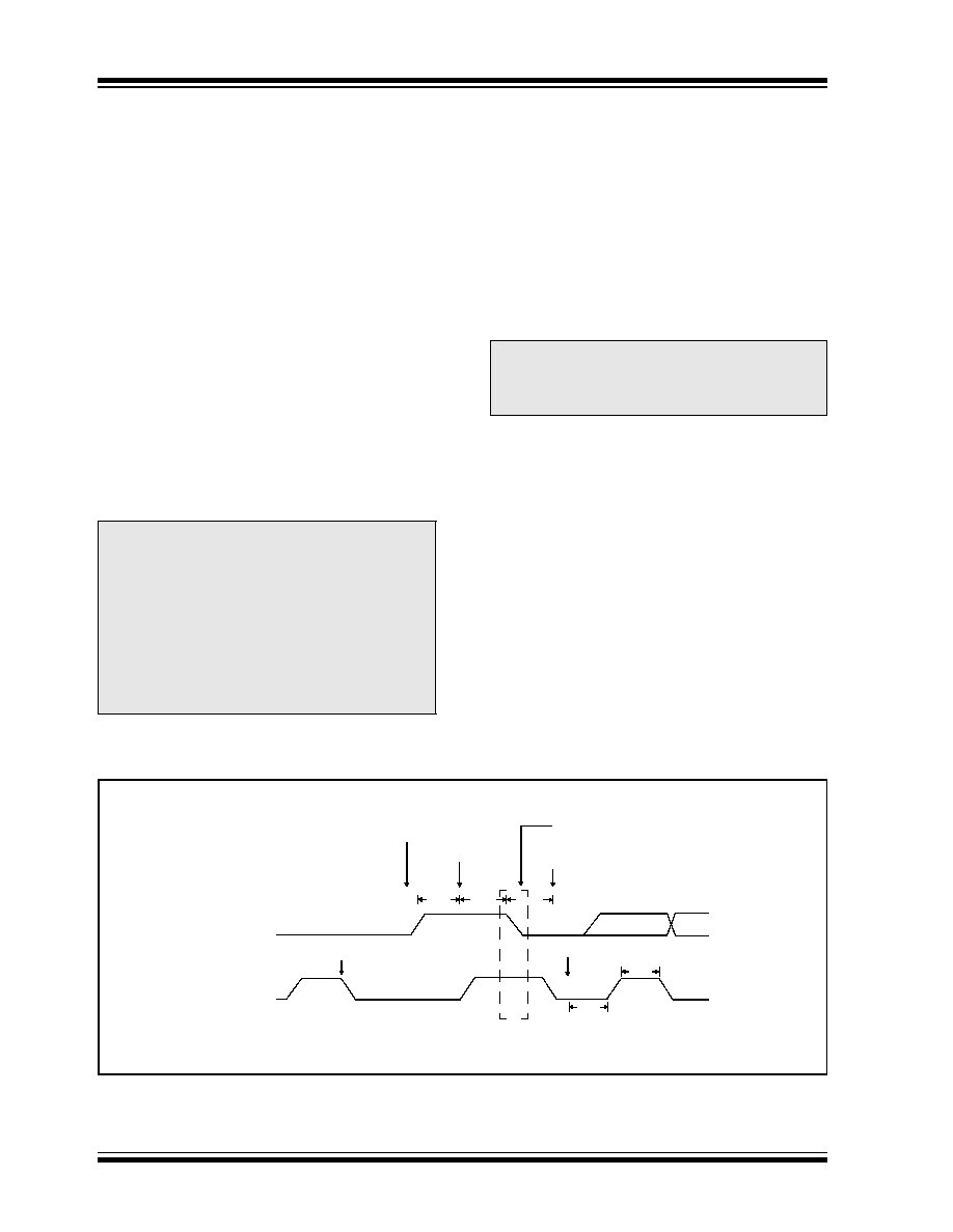
PIC18FXX8
DS41159B-page 170
Preliminary
2002 Microchip Technology Inc.
17.4.9
I
2
C MASTER MODE REPEATED
START CONDITION TIMING
A Repeated START condition occurs when the RSEN
bit (SSPCON2<1>) is programmed high and the I
2
C
logic module is in the IDLE state. When the RSEN bit is
set, the SCL pin is asserted low. When the SCL pin is
sampled low, the baud rate generator is loaded with the
contents of SSPADD<5:0> and begins counting. The
SDA pin is released (brought high) for one baud rate
generator count (T
BRG
). When the baud rate generator
times out, if SDA is sampled high, the SCL pin will be
de-asserted (brought high). When SCL is sampled
high, the baud rate generator is reloaded with the con-
tents of SSPADD<6:0> and begins counting. SDA and
SCL must be sampled high for one T
BRG
. This action is
then followed by assertion of the SDA pin (SDA = 0) for
one T
BRG,
while SCL is high. Following this, the RSEN
bit (SSPCON2<1>) will be automatically cleared and
the baud rate generator will not be reloaded, leaving
the SDA pin held low. As soon as a START condition is
detected on the SDA and SCL pins, the S bit
(SSPSTAT<3>) will be set. The SSPIF bit will not be set
until the baud rate generator has timed out.
Immediately following the SSPIF bit getting set, the
user may write the SSPBUF with the 7-bit address in
7-bit mode, or the default first address in 10-bit mode.
After the first eight bits are transmitted and an ACK is
received, the user may then transmit an additional eight
bits of address (10-bit mode) or eight bits of data (7-bit
mode).
17.4.9.1
WCOL Status Flag
If the user writes the SSPBUF when a Repeated
START sequence is in progress, the WCOL is set and
the contents of the buffer are unchanged (the write
doesn't occur).
FIGURE 17-20:
REPEAT START CONDITION WAVEFORM
Note 1: If RSEN is programmed while any other
event is in progress, it will not take effect.
2: A bus collision during the Repeated
START condition occurs if:
� SDA is sampled low when SCL goes
from low to high.
� SCL goes low before SDA is
asserted low. This may indicate that
another master is attempting to
transmit a data "1".
Note:
Because queueing of events is not
allowed, writing of the lower 5 bits of
SSPCON2 is disabled until the Repeated
START condition is complete.
SDA
SCL
Sr = Repeated START
Write to SSPCON2
Write to SSPBUF occurs here
Falling edge of ninth clock
End of Xmit
At completion of START bit,
hardware clear RSEN bit
1st bit
Set S (SSPSTAT<3>)
T
BRG
T
BRG
SDA = 1,
SDA = 1,
SCL (no change)
SCL = 1
occurs here.
T
BRG
T
BRG
T
BRG
and set SSPIF

2002 Microchip Technology Inc.
Preliminary
DS41159B-page 171
PIC18FXX8
17.4.10
I
2
C MASTER MODE
TRANSMISSION
Transmission of a data byte, a 7-bit address, or the
other half of a 10-bit address is accomplished by simply
writing a value to the SSPBUF register. This action will
set the buffer full flag bit, BF, and allow the baud rate
generator to begin counting and start the next transmis-
sion. Each bit of address/data will be shifted out onto
the SDA pin after the falling edge of SCL is asserted
(see data hold time specification parameter 106). SCL
is held low for one baud rate generator rollover count
(T
BRG
). Data should be valid before SCL is released
high (see data setup time specification parameter 107).
When the SCL pin is released high, it is held that way
for T
BRG
. The data on the SDA pin must remain stable
for that duration and some hold time after the next fall-
ing edge of SCL. After the eighth bit is shifted out (the
falling edge of the eighth clock), the BF flag is cleared
and the master releases SDA. This allows the slave
device being addressed to respond with an ACK bit
during the ninth bit time if an address match occurred
or if data was received properly. The status of ACK is
written into the ACKDT bit on the falling edge of the
ninth clock. If the master receives an Acknowledge, the
Acknowledge status bit, ACKSTAT, is cleared. If not,
the bit is set. After the ninth clock, the SSPIF bit is set
and the master clock (baud rate generator) is sus-
pended until the next data byte is loaded into the
SSPBUF, leaving SCL low and SDA unchanged
(Figure 17-21).
After the write to the SSPBUF, each bit of address will
be shifted out on the falling edge of SCL until all seven
address bits and the R/W bit are completed. On the fall-
ing edge of the eighth clock, the master will de-assert
the SDA pin, allowing the slave to respond with an
Acknowledge. On the falling edge of the ninth clock, the
master will sample the SDA pin to see if the address
was recognized by a slave. The status of the ACK bit is
loaded into the ACKSTAT status bit (SSPCON2<6>).
Following the falling edge of the ninth clock transmis-
sion of the address, the SSPIF is set, the BF flag is
cleared and the baud rate generator is turned off until
another write to the SSPBUF takes place, holding SCL
low and allowing SDA to float.
17.4.10.1
BF Status Flag
In Transmit mode, the BF bit (SSPSTAT<0>) is set
when the CPU writes to SSPBUF and is cleared when
all 8 bits are shifted out.
17.4.10.2
WCOL Status Flag
If the user writes the SSPBUF when a transmit is
already in progress (i.e., SSPSR is still shifting out a
data byte), the WCOL is set and the contents of the
buffer are unchanged (the write doesn't occur).
WCOL must be cleared in software.
17.4.10.3
ACKSTAT Status Flag
In Transmit mode, the ACKSTAT bit (SSPCON2<6>) is
cleared when the slave has sent an Acknowledge
(ACK = 0), and is set when the slave does not Acknowl-
edge (ACK = 1). A slave sends an Acknowledge when
it has recognized its address (including a general call),
or when the slave has properly received its data.
17.4.11
I
2
C MASTER MODE RECEPTION
Master mode reception is enabled by programming the
receive enable bit, RCEN (SSPCON2<3>).
The baud rate generator begins counting, and on each
rollover, the state of the SCL pin changes (high to
low/low to high) and data is shifted into the SSPSR.
After the falling edge of the eighth clock, the receive
enable flag is automatically cleared, the contents of the
SSPSR are loaded into the SSPBUF, the BF flag bit is
set, the SSPIF flag bit is set and the baud rate genera-
tor is suspended from counting, holding SCL low. The
MSSP is now in IDLE state, awaiting the next com-
mand. When the buffer is read by the CPU, the BF flag
bit is automatically cleared. The user can then send an
Acknowledge bit at the end of reception, by setting the
Acknowledge sequence enable bit, ACKEN
(SSPCON2<4>).
17.4.11.1
BF Status Flag
In receive operation, the BF bit is set when an address
or data byte is loaded into SSPBUF from SSPSR. It is
cleared when the SSPBUF register is read.
17.4.11.2
SSPOV Status Flag
In receive operation, the SSPOV bit is set when 8 bits
are received into the SSPSR and the BF flag bit is
already set from a previous reception.
17.4.11.3
WCOL Status Flag
If the user writes the SSPBUF when a receive is
already in progress (i.e., SSPSR is still shifting in a data
byte), the WCOL bit is set and the contents of the buffer
are unchanged (the write doesn't occur).
Note:
The RCEN bit should be set after ACK
sequence is complete, or the RCEN bit will
be disregarded.
PIC18FXX8
DS41159B-page 172
Preliminary
2002 Microchip Technology Inc.
FIGURE 17-21:
I
2
C MASTER MODE WAVEFORM (TRANSMISSION, 7 OR 10-BIT ADDRESS)
SDA
SCL
SSPI
F
BF (
SSPST
A
T
<0
>)
SEN
A7
A
6
A5
A4
A
3
A
2
A1
A
C
K
=
0
D
7D
6
D
5
D
4
D
3
D
2D
1
D
0
ACK
T
r
an
smi
t
ti
ng
D
a
t
a
or
S
e
co
nd
H
a
l
f
R/
W
=
0
T
r
an
smi
t
A
d
dr
ess t
o
S
l
ave
1
2
3
4
56
789
12
3
4
5
6
7
8
9
P
Cle
a
r
e
d
in
so
ftwa
r
e
se
r
v
ice
r
o
u
t
in
e
SSPBUF
i
s
wr
it
t
e
n
i
n
s
o
f
t
w
a
r
e
Fr
o
m
SSP in
t
e
r
r
u
p
t
A
f
t
e
r S
T
A
R
T
co
ndi
t
i
on,
S
E
N
cl
ear
ed
by h
a
r
d
w
a
r
e
S
SSPBUF
wr
it
t
e
n
wit
h
7
-
b
i
t
a
d
d
r
e
s
s
a
n
d
R/
W
star
t tra
n
sm
it
SCL
h
e
ld
l
o
w
wh
ile
CPU
r
e
s
p
o
n
d
s
t
o
SSPI
F
SEN = 0
o
f
10
-b
i
t
A
ddr
ess
W
r
it
e
SSPCO
N
2
<
0
>
SEN = 1
S
T
A
R
T c
o
n
d
i
t
i
on
be
gi
ns
F
r
om
sl
a
v
e cl
e
a
r
A
C
K
S
T
A
T
bi
t
S
S
P
C
ON
2<
6>
ACKST
A
T
in
SSPCO
N
2
= 1
C
l
e
a
r
ed i
n
so
ftw
ar
e
SS
PBUF wr
it
t
e
n
PEN
Cle
a
r
e
d
in
so
ft
wa
r
e
R/
W
2002 Microchip Technology Inc.
Preliminary
DS41159B-page 173
PIC18FXX8
FIGURE 17-22:
I
2
C MASTER MODE WAVEFORM (RECEPTION, 7-BIT ADDRESS)
P
9
8
7
6
5
D0
D1
D2
D3
D4
D5
D6
D7
S
A7
A6
A5
A4
A3
A2
A1
SDA
SCL
12
3
4
5
6
7
8
9
12
3
4
5
67
8
9
12
3
4
B
u
s M
a
ster
ter
m
i
nate
s
tra
n
sfer
AC
K
Re
ce
ivin
g
Da
ta
fr
o
m
Sl
a
v
e
Re
ce
ivin
g
Da
t
a
fr
o
m
Sla
v
e
D0
D1
D2
D3
D4
D5
D6
D7
ACK
R/W
= 1
T
r
a
n
smi
t
A
ddr
ess to S
l
ave
SSPI
F
BF
AC
K
i
s
not
sent
W
r
i
t
e t
o
S
S
P
C
ON
2<
0>
(S
E
N
=
1)
W
r
i
t
e
to S
S
P
B
U
F occu
rs her
e
A
C
K f
r
o
m
Sl
a
v
e
M
a
ster
confi
g
ured
as a r
e
cei
v
er
b
y
pro
g
ram
m
i
ng
S
S
P
C
ON
2<
3>
, (R
C
E
N
=
1)
PE
N b
i
t
=
1
w
r
i
tte
n her
e
D
a
t
a
sh
i
f
ted i
n
o
n
fal
l
i
ng
edge o
f
C
L
K
C
l
ear
ed i
n
so
ftw
are
S
t
art X
M
IT
SEN =
0
SSPO
V
SDA =
0
,
SCL
= 1
wh
i
l
e
CP
U
(
S
S
PST
A
T
<0
>)
AC
K
La
st bit is shifte
d into
S
S
P
S
R an
d
con
t
ent
s ar
e unl
oa
ded i
n
to S
S
P
B
U
F
Cle
a
r
e
d
in
so
ft
w
a
r
e
C
l
ea
r
e
d i
n
s
o
f
t
w
ar
e
S
e
t S
S
P
I
F
in
terr
upt
at en
d of r
e
cei
v
e
Se
t
P b
i
t
(
SSP
ST
A
T
<4
>)
an
d S
S
P
I
F
C
l
ear
ed i
n
soft
w
a
r
e
A
C
K
fro
m
Ma
ster
Se
t
SS
PI
F a
t
e
n
d
S
e
t S
S
P
IF
inter
r
up
t
at
end o
f
A
cknow
l
edge
se
quence
Se
t
SS
PI
F in
t
e
r
r
u
p
t
at e
nd of
A
ckno
w
-
l
edge
seque
nce
of r
e
ceive
S
e
t A
C
K
E
N
,
st
ar
t A
cknow
l
edg
e sequ
ence
S
S
P
O
V
i
s
set
beca
u
se
S
SPB
UF
is still fu
ll
S
D
A = ACK
D
T = 1
RCEN cle
a
r
e
d
a
u
tom
a
tically
RCEN = 1
st
a
r
t
ne
xt r
e
ce
ive
W
r
i
t
e to
S
S
P
C
ON
2<
4>
to st
ar
t A
cknow
l
edge
seque
nce
SD
A = ACK
D
T (
SSP
CO
N2
<5
>)
= 0
RCEN cle
a
r
e
d
a
u
tom
a
tically
r
e
spon
ds to S
S
P
I
F
ACKEN
Be
g
i
n
ST
AR
T
Co
n
d
itio
n
C
l
ear
ed i
n
so
ftw
are
SDA = A
C
KDT
= 0
PIC18FXX8
DS41159B-page 174
Preliminary
2002 Microchip Technology Inc.
17.4.12
ACKNOWLEDGE SEQUENCE
TIMING
An Acknowledge sequence is enabled by setting the
Acknowledge sequence enable bit, ACKEN
(SSPCON2<4>). When this bit is set, the SCL pin is
pulled low and the contents of the Acknowledge data bit
are presented on the SDA pin. If the user wishes to gen-
erate an Acknowledge, then the ACKDT bit should be
cleared. If not, the user should set the ACKDT bit before
starting an Acknowledge sequence. The baud rate gen-
erator then counts for one rollover period (T
BRG
) and the
SCL pin is de-asserted (pulled high). When the SCL pin
is sampled high (clock arbitration), the baud rate gener-
ator counts for T
BRG
. The SCL pin is then pulled low. Fol-
lowing this, the ACKEN bit is automatically cleared, the
baud rate generator is turned off and the MSSP module
then goes into IDLE mode (Figure 17-23).
17.4.12.1
WCOL Status Flag
If the user writes the SSPBUF when an Acknowledge
sequence is in progress, then WCOL is set and the con-
tents of the buffer are unchanged (the write doesn't occur).
17.4.13
STOP CONDITION TIMING
A STOP bit is asserted on the SDA pin at the end of a
receive/transmit by setting the STOP sequence enable
bit, PEN (SSPCON2<2>). At the end of a receive/trans-
mit the SCL line is held low after the falling edge of the
ninth clock. When the PEN bit is set, the master will
assert the SDA line low. When the SDA line is sampled
low, the baud rate generator is reloaded and counts
down to 0. When the baud rate generator times out, the
SCL pin will be brought high, and one T
BRG
(baud rate
generator rollover count) later, the SDA pin will be
de-asserted. When the SDA pin is sampled high while
SCL is high, the P bit (SSPSTAT<4>) is set. A T
BRG
later, the PEN bit is cleared and the SSPIF bit is set
(Figure 17-24).
17.4.13.1
WCOL Status Flag
If the user writes the SSPBUF when a STOP sequence
is in progress, then the WCOL bit is set and the con-
tents of the buffer are unchanged (the write doesn't
occur).
FIGURE 17-23:
ACKNOWLEDGE SEQUENCE WAVEFORM
Note: T
BRG
= one baud rate generator period.
SDA
SCL
Set SSPIF at the end
Acknowledge sequence starts here,
Write to SSPCON2
ACKEN automatically cleared
Cleared in
T
BRG
T
BRG
of receive
ACK
8
ACKEN = 1, ACKDT = 0
D0
9
SSPIF
software
Set SSPIF at the end
of Acknowledge sequence
Cleared in
software
2002 Microchip Technology Inc.
Preliminary
DS41159B-page 175
PIC18FXX8
FIGURE 17-24:
STOP CONDITION RECEIVE OR TRANSMIT MODE
17.4.14
SLEEP OPERATION
While in SLEEP mode, the I
2
C module can receive
addresses or data, and when an address match or
complete byte transfer occurs, wake the processor
from SLEEP (if the MSSP interrupt is enabled).
17.4.15
EFFECT OF A RESET
A RESET disables the MSSP module and terminates
the current transfer.
17.4.16
MULTI-MASTER MODE
In Multi-Master mode, the interrupt generation on the
detection of the START and STOP conditions allows
the determination of when the bus is free. The STOP
(P) and START (S) bits are cleared from a RESET or
when the MSSP module is disabled. Control of the I
2
C
bus may be taken when the P bit (SSPSTAT<4>) is set,
or the bus is idle with both the S and P bits clear. When
the bus is busy, enabling the SSP interrupt will gener-
ate the interrupt when the STOP condition occurs.
In multi-master operation, the SDA line must be moni-
tored for arbitration, to see if the signal level is the
expected output level. This check is performed in
hardware, with the result placed in the BCLIF bit.
The states where arbitration can be lost are:
� Address Transfer
� Data Transfer
� A START Condition
� A Repeated START Condition
� An Acknowledge Condition
17.4.17
MULTI -MASTER
COMMUNICATION, BUS COLLISION
AND BUS ARBITRATION
Multi-Master mode support is achieved by bus arbitra-
tion. When the master outputs address/data bits onto
the SDA pin, arbitration takes place when the master
outputs a '1' on SDA, by letting SDA float high and
another master asserts a '0'. When the SCL pin floats
high, data should be stable. If the expected data on
SDA is a '1' and the data sampled on the SDA pin = '0',
then a bus collision has taken place. The master will set
the Bus Collision Interrupt Flag BCLIF and reset the I
2
C
port to its IDLE state (Figure 17-25).
If a transmit was in progress when the bus collision
occurred, the transmission is halted, the BF flag is
cleared, the SDA and SCL lines are de-asserted, and
the SSPBUF can be written to. When the user services
the bus collision Interrupt Service Routine, and if the
I
2
C bus is free, the user can resume communication by
asserting a START condition.
If a START, Repeated START, STOP, or Acknowledge
condition was in progress when the bus collision
occurred, the condition is aborted, the SDA and SCL
lines are de-asserted, and the respective control bits in
the SSPCON2 register are cleared. When the user ser-
vices the bus collision Interrupt Service Routine, and if
the I
2
C bus is free, the user can resume communication
by asserting a START condition.
The master will continue to monitor the SDA and SCL
pins. If a STOP condition occurs, the SSPIF bit will be set.
A write to the SSPBUF will start the transmission of
data at the first data bit, regardless of where the trans-
mitter left off when the bus collision occurred.
In Multi-Master mode, the interrupt generation on the
detection of START and STOP conditions allows the
determination of when the bus is free. Control of the I
2
C
bus can be taken when the P bit is set in the SSPSTAT
register, or the bus is IDLE and the S and P bits are
cleared.
SCL
SDA
SDA asserted low before rising edge of clock
Write to SSPCON2
Set PEN
Falling edge of
SCL = 1 for T
BRG
, followed by SDA = 1 for T
BRG
9th clock
SCL brought high after T
BRG
Note: T
BRG
= one baud rate generator period.
T
BRG
T
BRG
after SDA sampled high. P bit (SSPSTAT<4>) is set.
T
BRG
to setup STOP condition
.
ACK
P
T
BRG
PEN bit (SSPCON2<2>) is cleared by
hardware and the SSPIF bit is set
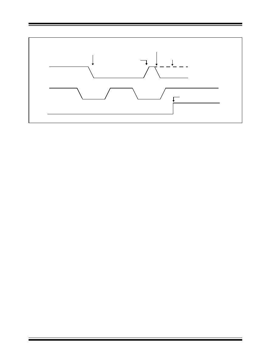
PIC18FXX8
DS41159B-page 176
Preliminary
2002 Microchip Technology Inc.
FIGURE 17-25:
BUS COLLISION TIMING FOR TRANSMIT AND ACKNOWLEDGE
SDA
SCL
BCLIF
SDA released
SDA line pulled low
by another source
Sample SDA. While SCL is high,
data doesn't match what is driven
Bus collision has occurred.
Set bus collision
interrupt (BCLIF)
by the master.
by master
Data changes
while SCL = 0
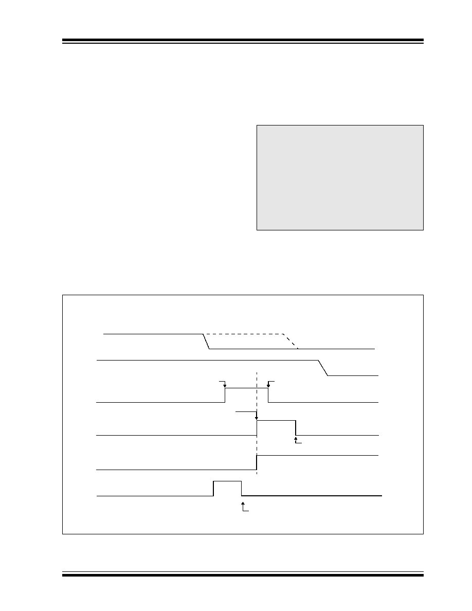
2002 Microchip Technology Inc.
Preliminary
DS41159B-page 177
PIC18FXX8
17.4.17.1
Bus Collision During a START
Condition
During a START condition, a bus collision occurs if:
a)
SDA or SCL are sampled low at the beginning of
the START condition (Figure 17-26).
b)
SCL is sampled low before SDA is asserted low
(Figure 17-27).
During a START condition, both the SDA and the SCL
pins are monitored.
If the SDA pin is already low, or the SCL pin is already
low, then all of the following occur:
� the START condition is aborted,
� the BCLIF flag is set, and
� the MSSP module is reset to its IDLE state
(Figure 17-26).
The START condition begins with the SDA and SCL
pins de-asserted. When the SDA pin is sampled high,
the baud rate generator is loaded from SSPADD<6:0>
and counts down to 0. If the SCL pin is sampled low
while SDA is high, a bus collision occurs, because it is
assumed that another master is attempting to drive a
data '1' during the START condition.
If the SDA pin is sampled low during this count, the
BRG is reset and the SDA line is asserted early
(Figure 17-28). If, however, a '1' is sampled on the SDA
pin, the SDA pin is asserted low at the end of the BRG
count. The baud rate generator is then reloaded and
counts down to 0, and during this time, if the SCL pins
are sampled as '0', a bus collision does not occur. At
the end of the BRG count, the SCL pin is asserted low.
FIGURE 17-26:
BUS COLLISION DURING START CONDITION (SDA ONLY)
Note:
The reason that bus collision is not a factor
during a START condition is that no two
bus masters can assert a START condition
at the exact same time. Therefore, one
master will always assert SDA before the
other. This condition does not cause a bus
collision, because the two masters must be
allowed to arbitrate the first address follow-
ing the START condition. If the address is
the same, arbitration must be allowed to
continue into the data portion, Repeated
START or STOP conditions.
SDA
SCL
SEN
SDA sampled low before
SDA goes low before the SEN bit is set.
S bit and SSPIF set because
SSP module reset into IDLE state.
SEN cleared automatically because of bus collision.
S bit and SSPIF set because
Set SEN, enable START
condition if SDA = 1, SCL=1
SDA = 0, SCL = 1.
BCLIF
S
SSPIF
SDA = 0, SCL = 1.
SSPIF and BCLIF are
cleared in software.
SSPIF and BCLIF are
cleared in software.
Set BCLIF,
Set BCLIF.
START condition.
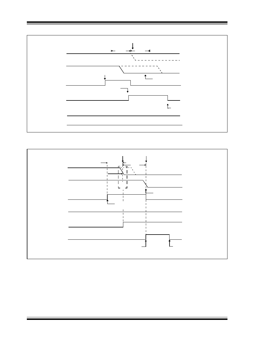
PIC18FXX8
DS41159B-page 178
Preliminary
2002 Microchip Technology Inc.
FIGURE 17-27:
BUS COLLISION DURING START CONDITION (SCL = 0)
FIGURE 17-28:
BRG RESET DUE TO SDA ARBITRATION DURING START CONDITION
SDA
SCL
SEN
bus collision occurs. Set BCLIF.
SCL = 0 before SDA = 0,
Set SEN, enable START
sequence if SDA = 1, SCL = 1
T
BRG
T
BRG
SDA = 0, SCL = 1
BCLIF
S
SSPIF
Interrupt cleared
in software
bus collision occurs. Set BCLIF.
SCL = 0 before BRG time-out,
'0'
'0'
'0'
'0'
SDA
SCL
SEN
Set S
Set SEN, enable START
sequence if SDA = 1, SCL = 1
Less than T
BRG
T
BRG
SDA = 0, SCL = 1
BCLIF
S
SSPIF
S
Interrupts cleared
in software
Set SSPIF
SDA = 0, SCL = 1
SDA pulled low by other master.
Reset BRG and assert SDA.
SCL pulled low after BRG
Time-out
Set SSPIF
'0'
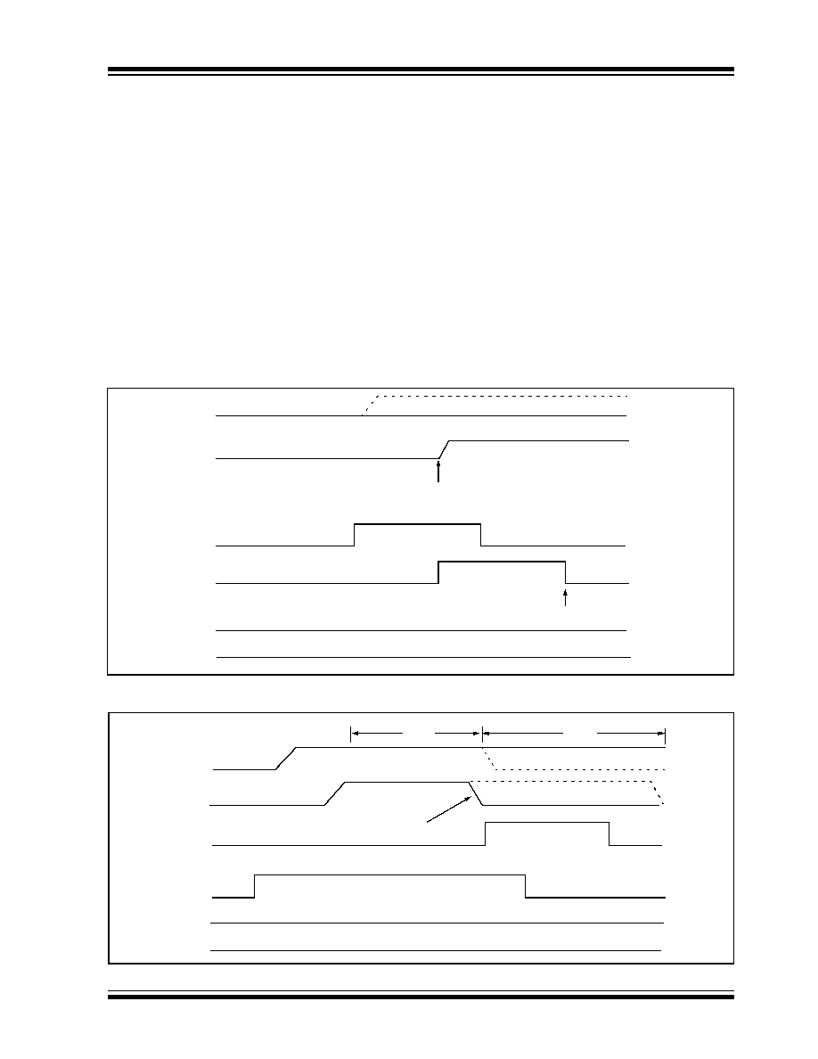
2002 Microchip Technology Inc.
Preliminary
DS41159B-page 179
PIC18FXX8
17.4.17.2
Bus Collision During a Repeated
START Condition
During a Repeated START condition, a bus collision
occurs if:
a)
A low level is sampled on SDA when SCL goes
from low level to high level.
b)
SCL goes low before SDA is asserted low, indi-
cating that another master is attempting to
transmit a data '1'.
When the user de-asserts SDA and the pin is allowed
to float high, the BRG is loaded with SSPADD<6:0>
and counts down to 0. The SCL pin is then de-asserted,
and when sampled high, the SDA pin is sampled.
If SDA is low, a bus collision has occurred (i.e., another
master is attempting to transmit a data '0',
Figure 17-29). If SDA is sampled high, the BRG is
reloaded and begins counting. If SDA goes from high to
low before the BRG times out, no bus collision occurs
because no two masters can assert SDA at exactly the
same time.
If SCL goes from high to low before the BRG times out
and SDA has not already been asserted, a bus collision
occurs. In this case, another master is attempting to
transmit a data '1' during the Repeated START
condition, Figure 17-30.
If, at the end of the BRG time-out both SCL and SDA
are still high, the SDA pin is driven low and the BRG is
reloaded and begins counting. At the end of the count,
regardless of the status of the SCL pin, the SCL pin is
driven low and the Repeated START condition is
complete.
FIGURE 17-29:
BUS COLLISION DURING A REPEATED START CONDITION (CASE 1)
FIGURE 17-30:
BUS COLLISION DURING REPEATED START CONDITION (CASE 2)
SDA
SCL
RSEN
BCLIF
S
SSPIF
Sample SDA when SCL goes high.
If SDA = 0, set BCLIF and release SDA and SCL.
Cleared in software
'0'
'0'
SDA
SCL
BCLIF
RSEN
S
SSPIF
Interrupt cleared
in software
SCL goes low before SDA,
Set BCLIF. Release SDA and SCL.
T
BRG
T
BRG
'0'
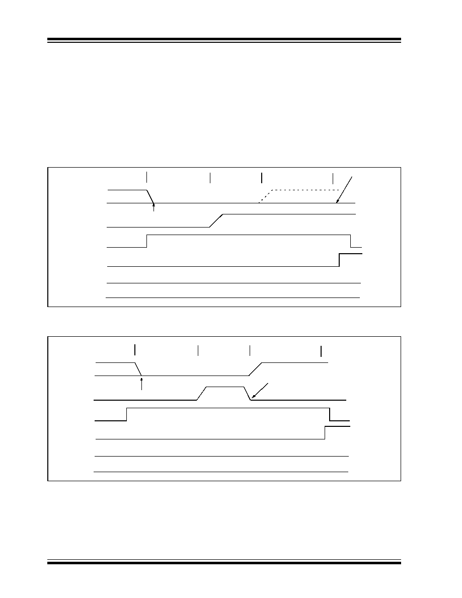
PIC18FXX8
DS41159B-page 180
Preliminary
2002 Microchip Technology Inc.
17.4.17.3
Bus Collision During a STOP
Condition
Bus collision occurs during a STOP condition if:
a)
After the SDA pin has been de-asserted and
allowed to float high, SDA is sampled low after
the BRG has timed out.
b)
After the SCL pin is de-asserted, SCL is sam-
pled low before SDA goes high.
The STOP condition begins with SDA asserted low.
When SDA is sampled low, the SCL pin is allowed to
float. When the pin is sampled high (clock arbitration),
the baud rate generator is loaded with SSPADD<6:0>
and counts down to 0. After the BRG times out, SDA is
sampled. If SDA is sampled low, a bus collision has
occurred. This is due to another master attempting to
drive a data '0' (Figure 17-31). If the SCL pin is sampled
low before SDA is allowed to float high, a bus collision
occurs. This is another case of another master
attempting to drive a data '0' (Figure 17-32).
FIGURE 17-31:
BUS COLLISION DURING A STOP CONDITION (CASE 1)
FIGURE 17-32:
BUS COLLISION DURING A STOP CONDITION (CASE 2)
SDA
SCL
BCLIF
PEN
P
SSPIF
T
BRG
T
BRG
T
BRG
SDA asserted low
SDA sampled
low after T
BRG
,
Set BCLIF
'0'
'0'
SDA
SCL
BCLIF
PEN
P
SSPIF
T
BRG
T
BRG
T
BRG
Assert SDA
SCL goes low before SDA goes high
Set BCLIF
'0'
'0'
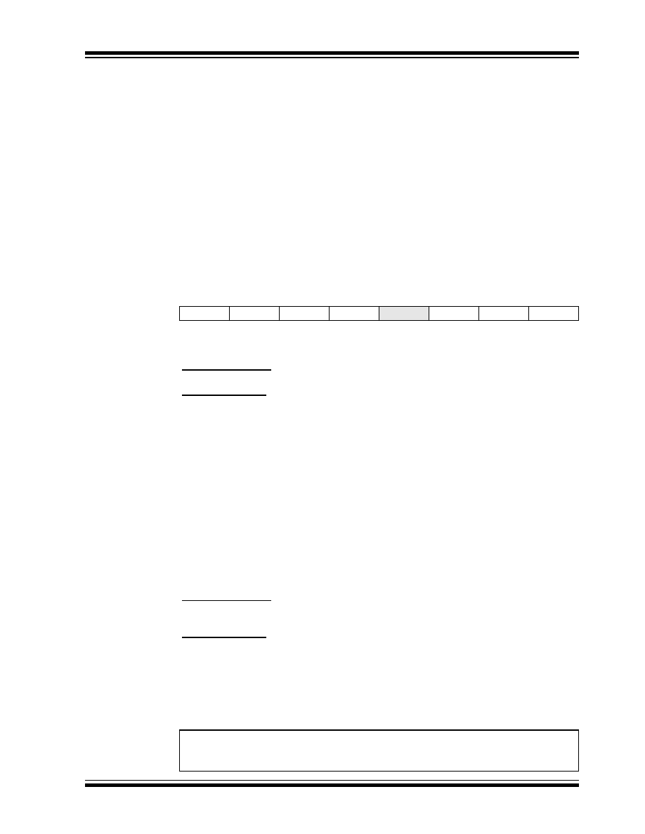
2002 Microchip Technology Inc.
Preliminary
DS41159B-page 181
PIC18FXX8
18.0
ADDRESSABLE UNIVERSAL
SYNCHRONOUS
ASYNCHRONOUS RECEIVER
TRANSMITTER (USART)
The Universal Synchronous Asynchronous Receiver
Transmitter (USART) module is one of the three serial
I/O modules incorporated into PIC18FXX8 devices.
(USART is also known as a Serial Communications
Interface or SCI.) The USART can be configured as a
full duplex asynchronous system that can communi-
cate with peripheral devices, such as CRT terminals
and personal computers, or it can be configured as a
half duplex synchronous system that can communicate
with peripheral devices, such as A/D or D/A integrated
circuits, Serial EEPROMs, etc.
The USART can be configured in the following modes:
� Asynchronous (full duplex)
� Synchronous - Master (half duplex)
� Synchronous - Slave (half duplex).
The SPEN (RCSTA register) and the TRISC<7> bits
have to be set and the TRISC<6> bit must be cleared,
in order to configure pins RC6/TX/CK and RC7/RX/DT
as the Universal Synchronous Asynchronous Receiver
Transmitter.
Register 18-1 shows the Transmit Status and Control
Register (TXSTA) and Register 18-2 shows the
Receive Status and Control Register (RCSTA).
REGISTER 18-1:
TXSTA REGISTER
R/W-0
R/W-0
R/W-0
R/W-0
U-0
R/W-0
R-1
R/W-0
CSRC
TX9
TXEN
SYNC
--
BRGH
TRMT
TX9D
bit 7
bit 0
bit 7
CSRC: Clock Source Select bit
Asynchronous mode:
Don't care
Synchronous mode:
1
= Master mode (Clock generated internally from BRG)
0
= Slave mode (Clock from external source)
bit 6
TX9: 9-bit Transmit Enable bit
1
= Selects 9-bit transmission
0
= Selects 8-bit transmission
bit 5
TXEN: Transmit Enable bit
1
= Transmit enabled
0
= Transmit disabled
Note:
SREN/CREN overrides TXEN in SYNC mode.
bit 4
SYNC: USART Mode Select bit
1
= Synchronous mode
0
= Asynchronous mode
bit 3
Unimplemented: Read as '0'
bit 2
BRGH: High Baud Rate Select bit
Asynchronous mode:
1
= High speed
0
= Low speed
Synchronous mode:
Unused in this mode
bit 1
TRMT: Transmit Shift Register Status bit
1
= TSR empty
0
= TSR full
bit 0
TX9D: 9th bit of Transmit Data
Can be address/data bit or a parity bit
Legend:
R = Readable bit
W = Writable bit
U = Unimplemented bit, read as `0'
- n = Value at POR
'1' = Bit is set
'0' = Bit is cleared
x = Bit is unknown

PIC18FXX8
DS41159B-page 182
Preliminary
2002 Microchip Technology Inc.
REGISTER 18-2:
RCSTA REGISTER
R/W-0
R/W-0
R/W-0
R/W-0
R/W-0
R-0
R-0
R-x
SPEN
RX9
SREN
CREN
ADDEN
FERR
OERR
RX9D
bit 7
bit 0
bit 7
SPEN: Serial Port Enable bit
1
= Serial port enabled (configures RX/DT and TX/CK pins as serial port pins)
0
= Serial port disabled
bit 6
RX9: 9-bit Receive Enable bit
1
= Selects 9-bit reception
0
= Selects 8-bit reception
bit 5
SREN: Single Receive Enable bit
Asynchronous mode:
Don't care
Synchronous mode - Master:
1
= Enables single receive
0
= Disables single receive (this bit is cleared after reception is complete.)
Synchronous mode - Slave:
Unused in this mode
bit 4
CREN: Continuous Receive Enable bit
Asynchronous mode:
1
= Enables continuous receive
0
= Disables continuous receive
Synchronous mode:
1
= Enables continuous receive until enable bit CREN is cleared (CREN overrides SREN)
0
= Disables continuous receive
bit 3
ADDEN: Address Detect Enable bit
Asynchronous mode 9-bit (RX9 = 1):
1
= Enables address detection, enables interrupt and load of the receive buffer when RSR<8>
is set
0
= Disables address detection, all bytes are received, and ninth bit can be used as parity bit
bit 2
FERR: Framing Error bit
1
= Framing error (can be updated by reading RCREG register and receive next valid byte)
0
= No framing error
bit 1
OERR: Overrun Error bit
1
= Overrun error (can be cleared by clearing bit CREN)
0
= No overrun error
bit 0
RX9D: 9th bit of Received Data
Can be address/data bit or a parity bit
Legend:
R = Readable bit
W = Writable bit
U = Unimplemented bit, read as `0'
- n = Value at POR
'1' = Bit is set
'0' = Bit is cleared
x = Bit is unknown

2002 Microchip Technology Inc.
Preliminary
DS41159B-page 183
PIC18FXX8
18.1
USART Baud Rate Generator
(BRG)
The BRG supports both the Asynchronous and Syn-
chronous modes of the USART. It is a dedicated 8-bit
baud rate generator. The SPBRG register controls the
period of a free running 8-bit timer. In Asynchronous
mode, bit BRGH (TXSTA register) also controls the
baud rate. In Synchronous mode, bit BRGH is ignored.
Table 18-1 shows the formula for computation of the
baud rate for different USART modes, which only apply
in Master mode (internal clock).
Given the desired baud rate and F
OSC
, the nearest
integer value for the SPBRG register can be calculated
using the formula in Table 18-1. From this, the error in
baud rate can be determined.
Example 18-1 shows the calculation of the baud rate
error for the following conditions:
F
OSC
= 16 MHz
Desired Baud Rate = 9600
BRGH = 0
SYNC = 0
It may be advantageous to use the high baud rate
(BRGH = 1), even for slower baud clocks. This is
because the F
OSC
/(16(X + 1)) equation can reduce the
baud rate error in some cases.
Writing a new value to the SPBRG register causes the
BRG timer to be reset (or cleared). This ensures the
BRG does not wait for a timer overflow before
outputting the new baud rate.
18.1.1
SAMPLING
The data on the RC7/RX/DT pin is sampled three times
by a majority detect circuit to determine if a high or a
low level is present at the RX pin.
EXAMPLE 18-1:
CALCULATING BAUD RATE ERROR
TABLE 18-1:
BAUD RATE FORMULA
TABLE 18-2:
REGISTERS ASSOCIATED WITH BAUD RATE GENERATOR
Desired Baud Rate
= F
OSC
/ (64 (X + 1))
Solving for X:
X
= ( (F
OSC
/ Desired Baud Rate) / 64 ) - 1
X
= ((16000000 / 9600) / 64) - 1
X
= [25.042] = 25
Calculated Baud Rate
= 16000000 / (64 (25 + 1))
= 9615
Error
= (Calculated Baud Rate - Desired Baud Rate)
Desired Baud Rate
= (9615 - 9600) / 9600
= 0.16%
SYNC
BRGH = 0 (Low Speed)
BRGH = 1 (High Speed)
0
1
(Asynchronous) Baud Rate = F
OSC
/(64(X+1))
(Synchronous) Baud Rate = F
OSC
/(4(X+1))
Baud Rate = F
OSC
/(16(X+1))
NA
Legend: X = value in SPBRG (0 to 255)
Name
Bit 7
Bit 6
Bit 5
Bit 4
Bit 3
Bit 2
Bit 1
Bit 0
Value on
POR, BOR
Value on
all other
RESETS
TXSTA
CSRC
TX9
TXEN
SYNC
--
BRGH
TRMT
TX9D
0000 -010
0000 -010
RCSTA
SPEN
RX9
SREN
CREN
ADDEN
FERR
OERR
RX9D
0000 000x
0000 000x
SPBRG
Baud Rate Generator Register
0000 0000
0000 0000
Legend:
x
= unknown, - = unimplemented, read as '0'. Shaded cells are not used by the BRG.

PIC18FXX8
DS41159B-page 184
Preliminary
2002 Microchip Technology Inc.
TABLE 18-3:
BAUD RATES FOR SYNCHRONOUS MODE
BAUD
RATE
(Kbps)
F
OSC
= 40 MHz
SPBRG
value
(decimal)
33 MHz
SPBRG
value
(decimal)
25 MHz
SPBRG
value
(decimal)
20 MHz
SPBRG
value
(decimal)
KBAUD
%
ERROR
KBAUD
%
ERROR
KBAUD
%
ERROR
KBAUD
%
ERROR
0.3
NA
-
-
NA
-
-
NA
-
-
NA
-
-
1.2
NA
-
-
NA
-
-
NA
-
-
NA
-
-
2.4
NA
-
-
NA
-
-
NA
-
-
NA
-
-
9.6
NA
-
-
NA
-
-
NA
-
-
NA
-
-
19.2
NA
-
-
NA
-
-
NA
-
-
NA
-
-
76.8
76.92
+0.16
129
77.10
+0.39
106
77.16
+0.47
80
76.92
+0.16
64
96
96.15
+0.16
103
95.93
-0.07
85
96.15
+0.16
64
96.15
+0.16
51
300
303.03
+1.01
32
294.64
-1.79
27
297.62
-0.79
20
294.12
-1.96
16
500
500
0
19
485.30
-2.94
16
480.77
-3.85
12
500
0
9
HIGH
10000
-
0
8250
-
0
6250
-
0
5000
-
0
LOW
39.06
-
255
32.23
-
255
24.41
-
255
19.53
-
255
BAUD
RATE
(Kbps)
F
OSC
= 16 MHz
SPBRG
value
(decimal)
10 MHz
SPBRG
value
(decimal)
7.15909 MHz
SPBRG
value
(decimal)
5.0688 MHz
SPBRG
value
(decimal)
KBAUD
%
ERROR
KBAUD
%
ERROR
KBAUD
%
ERROR
KBAUD
%
ERROR
0.3
NA
-
-
NA
-
-
NA
-
-
NA
-
-
1.2
NA
-
-
NA
-
-
NA
-
-
NA
-
-
2.4
NA
-
-
NA
-
-
NA
-
-
NA
-
-
9.6 NA
-
-
NA
-
-
9.62
+0.23
185
9.60
0
131
19.2
19.23
+0.16
207
19.23
+0.16
129
19.24
+0.23
92
19.20
0
65
76.8
76.92
+0.16
51
75.76
-1.36
32
77.82
+1.32
22
74.54
-2.94
16
96
95.24
-0.79
41
96.15
+0.16
25
94.20
-1.88
18
97.48
+1.54
12
300
307.70
+2.56
12
312.50
+4.17
7
298.35
-0.57
5
316.80
+5.60
3
500
500
0
7
500
0
4
447.44
-10.51
3
422.40
-15.52
2
HIGH
4000
-
0
2500
-
0
1789.80
-
0
1267.20
-
0
LOW
15.63
-
255
9.77
-
255
6.99
-
255
4.95
-
255
BAUD
RATE
(Kbps)
F
OSC
= 4 MHz
SPBRG
value
(decimal)
3.579545 MHz
SPBRG
value
(decimal)
1 MHz
SPBRG
value
(decimal)
32.768 kHz
SPBRG
value
(decimal)
KBAUD
%
ERROR
KBAUD
%
ERROR
KBAUD
%
ERROR
KBAUD
%
ERROR
0.3
NA
-
-
NA
-
-
NA
-
-
0.30
+1.14
26
1.2
NA
-
-
NA
-
-
1.20
+0.16
207
1.17
-2.48
6
2.4
NA
-
-
NA
-
-
2.40
+0.16
103
2.73
+13.78
2
9.6
9.62
+0.16
103
9.62
+0.23
92
9.62
+0.16
25
8.20
-14.67
0
19.2
19.23
+0.16
51
19.04
-0.83
46
19.23
+0.16
12
NA
-
-
76.8
76.92
+0.16
12
74.57
-2.90
11
83.33
+8.51
2
NA
-
-
96
1000
+4.17
9
99.43
+3.57
8
83.33
-13.19
2
NA
-
-
300
333.33
+11.11
2
298.30
-0.57
2
250
-16.67
0
NA
-
-
500
500
0
1
447.44
-10.51
1
NA
-
-
NA
-
-
HIGH
1000
-
0
894.89
-
0
250
-
0
8.20
-
0
LOW
3.91
-
255
3.50
-
255
0.98
-
255
0.03
-
255

2002 Microchip Technology Inc.
Preliminary
DS41159B-page 185
PIC18FXX8
TABLE 18-4:
BAUD RATES FOR ASYNCHRONOUS MODE (BRGH = 0)
BAUD
RATE
(Kbps)
F
OSC
= 40 MHz
SPBRG
value
(decimal)
33 MHz
SPBRG
value
(decimal)
25 MHz
SPBRG
value
(decimal)
20 MHz
SPBRG
value
(decimal)
KBAUD
%
ERROR
KBAUD
%
ERROR
KBAUD
%
ERROR
KBAUD
%
ERROR
0.3
NA
-
-
NA
-
-
NA
-
-
NA
-
-
1.2 NA
-
-
NA
-
-
NA
-
-
NA
-
-
2.4 NA
-
-
2.40
-0.07
214
2.40
-0.15
162
2.40
+0.16
129
9.6 9.62
+0.16
64
9.55
-0.54
53
9.53
-0.76
40
9.47
-1.36
32
19.2
18.94
-1.36
32
19.10
-0.54
26
19.53
+1.73
19
19.53
+1.73
15
76.8
78.13
+1.73
7
73.66
-4.09
6
78.13
+1.73
4
78.13
+1.73
3
96
89.29
-6.99
6
103.13
+7.42
4
97.66
+1.73
3
104.17
+8.51
2
300
312.50
+4.17
1
257.81
-14.06
1
NA
-
-
312.50
+4.17
0
500
625
+25.00
0
NA
-
-
NA
-
-
NA
-
-
HIGH
625
-
0
515.63
-
0
390.63
-
0
312.50
-
0
LOW
2.44
-
255
2.01
-
255
1.53
-
255
1.22
-
255
BAUD
RATE
(Kbps)
F
OSC
= 16 MHz
SPBRG
value
(decimal)
10 MHz
SPBRG
value
(decimal)
7.15909 MHz
SPBRG
value
(decimal)
5.0688 MHz
SPBRG
value
(decimal)
KBAUD
%
ERROR
KBAUD
%
ERROR
KBAUD
%
ERROR
KBAUD
%
ERROR
0.3
NA -
-
NA -
-
NA
-
-
NA -
-
1.2 1.20
+0.16
207
1.20
+0.16
129
1.20
+0.23
92
1.20
0
65
2.4 2.40
+0.16
103
2.40
+0.16
64
2.38
-0.83
46
2.40
0
32
9.6 9.62
+0.16
25
9.77
+1.73
15
9.32
-2.90
11
9.90
+3.13
7
19.2
19.23
+0.16
12
19.53
+1.73
7
18.64
-2.90
5
19.80
+3.13
3
76.8
83.33
+8.51
2
78.13
+1.73
1
111.86
+45.65
0
79.20
+3.13
0
96
83.33
-13.19
2
78.13
-18.62
1
NA
-
-
NA
-
-
300
250
-16.67
0
156.25
-47.92
0
NA
-
-
NA
-
-
500
NA
-
-
NA
-
-
NA
-
-
NA
-
-
HIGH
250
-
0
156.25
-
0
111.86
-
0
79.20
-
0
LOW
0.98
-
255
0.61
-
255
0.44
-
255
0.31
-
255
BAUD
RATE
(Kbps)
F
OSC
= 4 MHz
SPBRG
value
(decimal)
3.579545 MHz
SPBRG
value
(decimal)
1 MHz
SPBRG
value
(decimal)
32.768 kHz
SPBRG
value
(decimal)
KBAUD
%
ERROR
KBAUD
%
ERROR
KBAUD
%
ERROR
KBAUD
%
ERROR
0.3
0.30
-0.16
207
0.30
+0.23
185
0.30
+0.16
51
0.26
-14.67
1
1.2 1.20
+1.67
51
1.19
-0.83
46
1.20
+0.16
12
NA
-
-
2.4 2.40
+1.67
25
2.43
+1.32
22
2.23
-6.99
6
NA
-
-
9.6 8.93
-6.99
6
9.32
-2.90
5
7.81
-18.62
1
NA
-
-
19.2
20.83
+8.51
2
18.64
-2.90
2
15.63
-18.62
0
NA
-
-
76.8
62.50
-18.62
0
55.93
-27.17
0
NA
-
-
NA
-
-
96
NA
-
-
NA
-
-
NA
-
-
NA
-
-
300
NA
-
-
NA
-
-
NA
-
-
NA
-
-
500
NA
-
-
NA
-
-
NA
-
-
NA
-
-
HIGH
62.50
-
0
55.93
-
0
15.63
-
0
0.51
-
0
LOW
0.24
-
255
0.22
-
255
0.06
-
255
0.002
-
255

PIC18FXX8
DS41159B-page 186
Preliminary
2002 Microchip Technology Inc.
TABLE 18-5:
BAUD RATES FOR ASYNCHRONOUS MODE (BRGH = 1)
BAUD
RATE
(Kbps)
F
OSC
= 40 MHz
SPBRG
value
(decimal)
33 MHz
SPBRG
value
(decimal)
25 MHz
SPBRG
value
(decimal)
20 MHz
SPBRG
value
(decimal)
KBAUD
%
ERROR
KBAUD
%
ERROR
KBAUD
%
ERROR
KBAUD
%
ERROR
0.3
NA
-
-
NA
-
-
NA
-
-
NA
-
-
1.2
NA
-
-
NA
-
-
NA
-
-
NA
-
-
2.4
NA
-
-
NA
-
-
NA
-
-
NA
-
-
9.6
NA
-
-
9.60
-0.07
214
9.59
-0.15
162
9.62
+0.16
129
19.2
19.23
+0.16
129
19.28
+0.39
106
19.30
+0.47
80
19.23
+0.16
64
76.8
75.76
-1.36
32
76.39
-0.54
26
78.13
+1.73
19
78.13
+1.73
15
96
96.15
+0.16
25
98.21
+2.31
20
97.66
+1.73
15
96.15
+0.16
12
300
312.50
+4.17
7
294.64
-1.79
6
312.50
+4.17
4
312.50
+4.17
3
500
500
0
4
515.63
+3.13
3
520.83
+4.17
2
416.67
-16.67
2
HIGH
2500
-
0
2062.50
-
0
1562.50
-
0
1250
-
0
LOW
9.77
-
255
8,06
-
255
6.10
-
255
4.88
-
255
BAUD
RATE
(Kbps)
F
OSC
= 16 MHz
SPBRG
value
(decimal)
10 MHz
SPBRG
value
(decimal)
7.15909 MHz
SPBRG
value
(decimal)
5.0688 MHz
SPBRG
value
(decimal)
KBAUD
%
ERROR
KBAUD
%
ERROR
KBAUD
%
ERROR
KBAUD
%
ERROR
0.3
NA
-
-
NA
-
-
NA
-
-
NA
-
-
1.2
NA
-
-
NA
-
-
NA
-
-
NA
-
-
2.4
NA
-
-
NA
-
-
2.41
+0.23
185
2.40
0
131
9.6
9.62
+0.16
103
9.62
+0.16
64
9.52
-0.83
46
9.60
0
32
19.2
19.23
+0.16
51
18.94
-1.36
32
19.45
+1.32
22
18.64
-2.94
16
76.8
76.92
+0.16
12
78.13
+1.73
7
74.57
-2.90
5
79.20
+3.13
3
96
100
+4.17
9
89.29
-6.99
6
89.49
-6.78
4
105.60
+10.00
2
300
333.33
+11.11
2
312.50
+4.17
1
447.44
+49.15
0
316.80
+5.60
0
500
500
0
1
625
+25.00
0
447.44
-10.51
0
NA
-
-
HIGH
1000
-
0
625
-
0
447.44
-
0
316.80
-
0
LOW
3.91
-
255
2.44
-
255
1.75
-
255
1.24
-
255
BAUD
RATE
(Kbps)
F
OSC
= 4 MHz
SPBRG
value
(decimal)
3.579545 MHz
SPBRG
value
(decimal)
1 MHz
SPBRG
value
(decimal)
32.768 kHz
SPBRG
value
(decimal)
KBAUD
%
ERROR
KBAUD
%
ERROR
KBAUD
%
ERROR
KBAUD
%
ERROR
0.3
NA
-
-
NA
-
-
0.30
+0.16
207
0.29
-2.48
6
1.2
1.20
+0.16
207
1.20
+0.23
185
1.20
+0.16
51
1.02
-14.67
1
2.4
2.40
+0.16
103
2.41
+0.23
92
2.40
+0.16
25
2.05
-14.67
0
9.6
9.62
+0.16
25
9.73
+1.32
22
8.93
-6.99
6
NA
-
-
19.2
19.23
+0.16
12
18.64
-2.90
11
20.83
+8.51
2
NA
-
-
76.8
NA
-
-
74.57
-2.90
2
62.50
-18.62
0
NA
-
-
96
NA
-
-
111.86
+16.52
1
NA
-
-
NA
-
-
300
NA
-
-
223.72
-25.43
0
NA
-
-
NA
-
-
500
NA
-
-
NA
-
-
NA
-
-
NA
-
-
HIGH
250
-
0
55.93
-
0
62.50
-
0
2.05
-
0
LOW
0.98
-
255
0.22
-
255
0.24
-
255
0.008
-
255
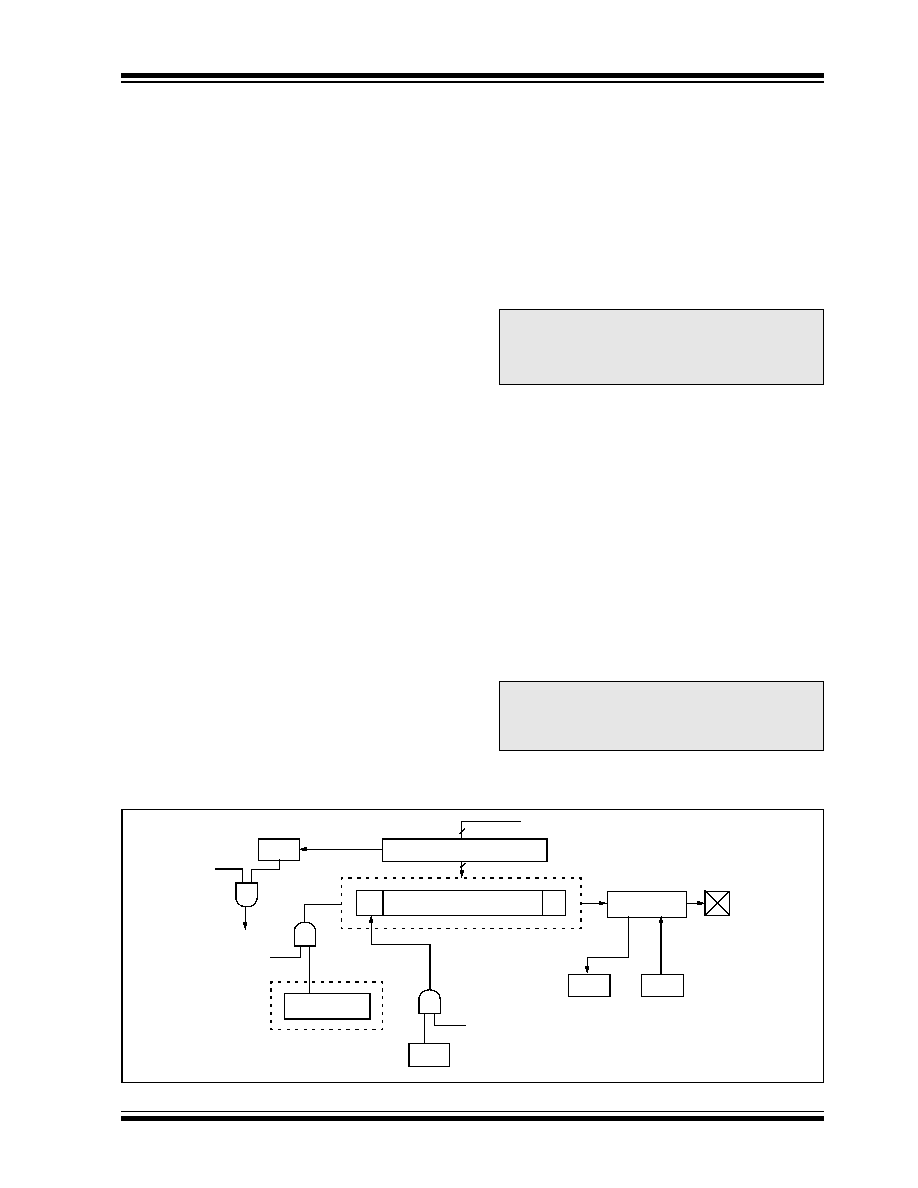
2002 Microchip Technology Inc.
Preliminary
DS41159B-page 187
PIC18FXX8
18.2
USART Asynchronous Mode
In this mode, the USART uses standard non-return-to-
zero (NRZ) format (one START bit, eight or nine data
bits and one STOP bit). The most common data format
is 8 bits. An on-chip dedicated 8-bit baud rate generator
can be used to derive standard baud rate frequencies
from the oscillator. The USART transmits and receives
the LSb first. The USART's transmitter and receiver are
functionally independent, but use the same data format
and baud rate. The baud rate generator produces a
clock, either x16 or x64 of the bit shift rate, depending
on the BRGH bit (TXSTA register). Parity is not sup-
ported by the hardware, but can be implemented in
software (and stored as the ninth data bit).
Asynchronous mode is stopped during SLEEP.
Asynchronous mode is selected by clearing the SYNC
bit (TXSTA register).
The USART Asynchronous module consists of the
following important elements:
� Baud Rate Generator
� Sampling Circuit
� Asynchronous Transmitter
� Asynchronous Receiver.
18.2.1
USART ASYNCHRONOUS
TRANSMITTER
The USART transmitter block diagram is shown in
Figure 18-1. The heart of the transmitter is the Transmit
(serial) Shift Register (TSR). The TSR register obtains
its data from the Read/Write Transmit Buffer register
(TXREG). The TXREG register is loaded with data in
software. The TSR register is not loaded until the STOP
bit has been transmitted from the previous load. As
soon as the STOP bit is transmitted, the TSR is loaded
with new data from the TXREG register (if available).
Once the TXREG register transfers the data to the TSR
register (occurs in one T
CY
), the TXREG register is
empty and flag bit TXIF (PIR registers) is set. This inter-
rupt can be enabled/disabled by setting/clearing
enable bit TXIE (PIE registers). Flag bit TXIF will be
set, regardless of the state of enable bit TXIE and can-
not be cleared in software. It will reset only when new
data is loaded into the TXREG register. While flag bit
TXIF indicated the status of the TXREG register,
another bit TRMT (TXSTA register) shows the status of
the TSR register. Status bit TRMT is a read only bit,
which is set when the TSR register is empty. No inter-
rupt logic is tied to this bit, so the user has to poll this
bit in order to determine if the TSR register is empty.
Steps to follow when setting up an Asynchronous
Transmission:
1.
Initialize the SPBRG register for the appropriate
baud rate. If a high speed baud rate is desired,
set bit BRGH (Section 18.1).
2.
Enable the asynchronous serial port by clearing
bit SYNC and setting bit SPEN.
3.
If interrupts are desired, set enable bit TXIE.
4.
If 9-bit transmission is desired, set transmit bit
TX9. Can be used as address/data bit.
5.
Enable the transmission by setting bit TXEN,
which will also set bit TXIF.
6.
If 9-bit transmission is selected, the ninth bit
should be loaded in bit TX9D.
7.
Load data to the TXREG register (starts
transmission).
FIGURE 18-1:
USART TRANSMIT BLOCK DIAGRAM
Note 1: The TSR register is not mapped in data
memory, so it is not available to the user.
2: Flag bit TXIF is set when enable bit TXEN
is set.
Note:
TXIF is not cleared immediately upon load-
ing data into the transmit buffer TXREG. The
flag bit becomes valid in the second instruc-
tion cycle following the load instruction.
TXIF
TXIE
Interrupt
TXEN
Baud Rate CLK
SPBRG
Baud Rate Generator
TX9D
MSb
LSb
Data Bus
TXREG register
TSR register
(8)
0
TX9
TRMT
SPEN
RC6/TX/CK pin
Pin Buffer
and Control
8
� � �
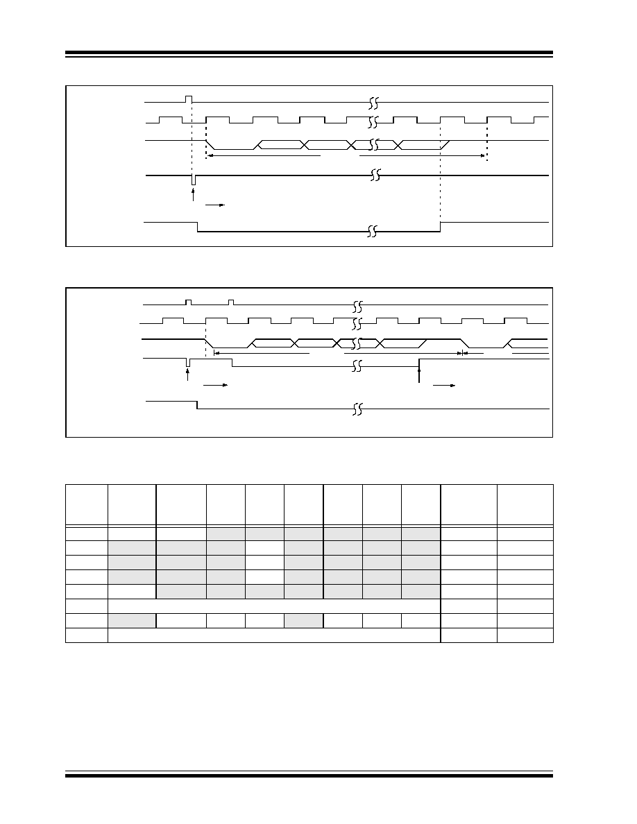
PIC18FXX8
DS41159B-page 188
Preliminary
2002 Microchip Technology Inc.
FIGURE 18-2:
ASYNCHRONOUS TRANSMISSION
FIGURE 18-3:
ASYNCHRONOUS TRANSMISSION (BACK TO BACK)
TABLE 18-6:
REGISTERS ASSOCIATED WITH ASYNCHRONOUS TRANSMISSION
Word 1
STOP bit
Word 1
Transmit Shift Reg
START bit
bit 0
bit 1
bit 7/8
Write to TXREG
Word 1
BRG Output
(Shift Clock)
RC6/TX/CK (pin)
TXIF bit
(Transmit Buffer
Register Empty Flag)
TRMT bit
(Transmit Shift
Register Empty Flag)
Transmit Shift Reg.
Write to TXREG
BRG Output
(Shift Clock)
RC6/TX/CK (pin)
TXIF bit
(Interrupt Reg. Flag)
TRMT bit
(Transmit Shift
Reg. Empty Flag)
Word 1
Word 2
Word 1
Word 2
START bit
STOP bit
START bit
Transmit Shift Reg.
Word 1
Word 2
bit 0
bit 1
bit 7/8
bit 0
Note: This timing diagram shows two consecutive transmissions.
Name
Bit 7
Bit 6
Bit 5
Bit 4
Bit 3
Bit 2
Bit 1
Bit 0
Value on
POR, BOR
Value on
all other
RESETS
INTCON GIE/GIEH PEIE/GIEL TMR0IE INT0IE
RBIE
TMR0IF INT0IF
RBIF
0000 000x 0000 000u
PIR1
PSPIF
ADIF
RCIF
TXIF
SSPIF
CCP1IF TMR2IF TMR1IF
0000 0000 0000 0000
PIE1
PSPIE
ADIE
RCIE
TXIE
SSPIE CCP1IE TMR2IE TMR1IE
0000 0000 0000 0000
IPR1
PSPIP
ADIP
RCIP
TXIP
SSPIP CCP1IP TMR2IP TMR1IP
0000 0000 0000 0000
RCSTA
SPEN
RX9
SREN
CREN
ADDEN
FERR
OERR
RX9D
0000 000x 0000 000x
TXREG
USART Transmit Register
0000 0000 0000 0000
TXSTA
CSRC
TX9
TXEN
SYNC
--
BRGH
TRMT
TX9D
0000 -010 0000 -010
SPBRG
Baud Rate Generator Register
0000 0000 0000 0000
Legend:
x
= unknown, - = unimplemented locations read as '0'.
Shaded cells are not used for Asynchronous Transmission.
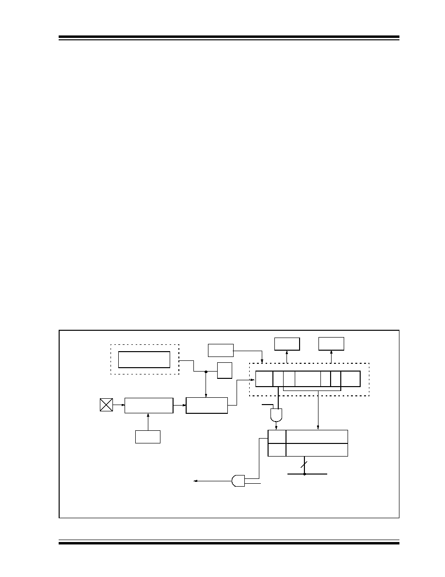
2002 Microchip Technology Inc.
Preliminary
DS41159B-page 189
PIC18FXX8
18.2.2
USART ASYNCHRONOUS
RECEIVER
The receiver block diagram is shown in Figure 18-4.
The data is received on the RC7/RX/DT pin and drives
the data recovery block. The data recovery block is
actually a high speed shifter, operating at x16 times the
baud rate, whereas the main receive serial shifter oper-
ates at the bit rate, or at F
OSC
. This mode would
typically be used in RS-232 systems.
Steps to follow when setting up an Asynchronous
Reception:
1.
Initialize the SPBRG register for the appropriate
baud rate. If a high speed baud rate is desired,
set bit BRGH (Section 18.1).
2.
Enable the asynchronous serial port by clearing
bit SYNC and setting bit SPEN.
3.
If interrupts are desired, set enable bit RCIE.
4.
If 9-bit reception is desired, set bit RX9.
5.
Enable the reception by setting bit CREN.
6.
Flag bit RCIF will be set when reception is com-
plete and an interrupt will be generated if enable
bit RCIE was set.
7.
Read the RCSTA register to get the ninth bit (if
enabled) and determine if any error occurred
during reception.
8.
Read the 8-bit received data by reading the
RCREG register.
9.
If any error occurred, clear the error by clearing
enable bit CREN.
18.2.3
SETTING UP 9-BIT MODE WITH
ADDRESS DETECT
This mode would typically be used in RS-485 systems.
Steps to follow when setting up an Asynchronous
Reception with Address Detect Enable:
1.
Initialize the SPBRG register for the appropriate
baud rate. If a high speed baud rate is required,
set the BRGH bit.
2.
Enable the asynchronous serial port by clearing
the SYNC bit and setting the SPEN bit.
3.
If interrupts are required, set the RCEN bit and
select the desired priority level with the RCIP bit.
4.
Set the RX9 bit to enable 9-bit reception.
5.
Set the ADDEN bit to enable address detect.
6.
Enable reception by setting the CREN bit.
7.
The RCIF bit will be set when reception is com-
plete. The interrupt will be Acknowledged if the
RCIE and GIE bits are set.
8.
Read the RCSTA register to determine if any
error occurred during reception, as well as read
bit 9 of data (if applicable).
9.
Read RCREG to determine if the device is being
addressed.
10. If any error occurred, clear the CREN bit.
11. If the device has been addressed, clear the
ADDEN bit to allow all received data into the
receive buffer and interrupt the CPU.
FIGURE 18-4:
USART RECEIVE BLOCK DIAGRAM
x64 Baud Rate CLK
SPBRG
Baud Rate Generator
RC7/RX/DT
Pin Buffer
and Control
SPEN
Data
Recovery
CREN
OERR
FERR
RSR Register
MSb
LSb
RX9D
RCREG Register
FIFO
Interrupt
RCIF
RCIE
Data Bus
8
�
64
�
16
or
STOP
START
(8)
7
1
0
RX9
� � �
Note:
I/O pins have diode protection to V
DD
and V
SS
.
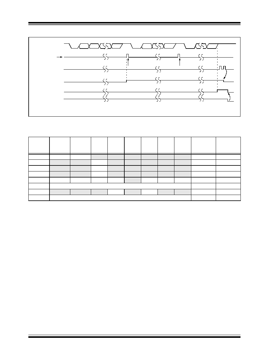
PIC18FXX8
DS41159B-page 190
Preliminary
2002 Microchip Technology Inc.
FIGURE 18-5:
ASYNCHRONOUS RECEPTION
TABLE 18-7:
REGISTERS ASSOCIATED WITH ASYNCHRONOUS RECEPTION
START
bit
bit7/8
bit1
bit0
bit7/8
bit0
STOP
bit
START
bit
START
bit
bit7/8
STOP
bit
RX (pin)
Reg
Rcv Buffer Reg
Rcv shift
Read Rcv
Buffer Reg
RCREG
RCIF
(Interrupt Flag)
OERR bit
CREN
Word 1
RCREG
Word 2
RCREG
STOP
bit
Note: This timing diagram shows three words appearing on the RX input. The RCREG (receive buffer) is read after the third word,
causing the OERR (overrun) bit to be set.
Name
Bit 7
Bit 6
Bit 5
Bit 4
Bit 3
Bit 2
Bit 1
Bit 0
Value on
POR, BOR
Value on
all other
RESETS
INTCON
GIE/GIEH
PEIE/GIEL TMR0IE
INT0IE
RBIE
TMR0IF
INT0IF
RBIF
0000 000x
0000 000u
PIR1
PSPIF
ADIF
RCIF
TXIF
SSPIF
CCP1IF
TMR2IF
TMR1IF
0000 0000
0000 0000
PIE1
PSPIE
ADIE
RCIE
TXIE
SSPIE
CCP1IE
TMR2IE
TMR1IE
0000 0000
0000 0000
IPR1
PSPIP
ADIP
RCIP
TXIP
SSPIP
CCP1IP
TMR2IP
TMR1IP
0000 0000
0000 0000
RCSTA
SPEN
RX9
SREN
CREN
ADDEN
FERR
OERR
RX9D
0000 000x
0000 000x
RCREG
USART Receive Register
0000 0000
0000 0000
TXSTA
CSRC
TX9
TXEN
SYNC
--
BRGH
TRMT
TX9D
0000 -010
0000 -010
SPBRG
Baud Rate Generator Register
0000 0000
0000 0000
Legend:
x
= unknown, - = unimplemented locations read as '0'. Shaded cells are not used for Asynchronous Reception.
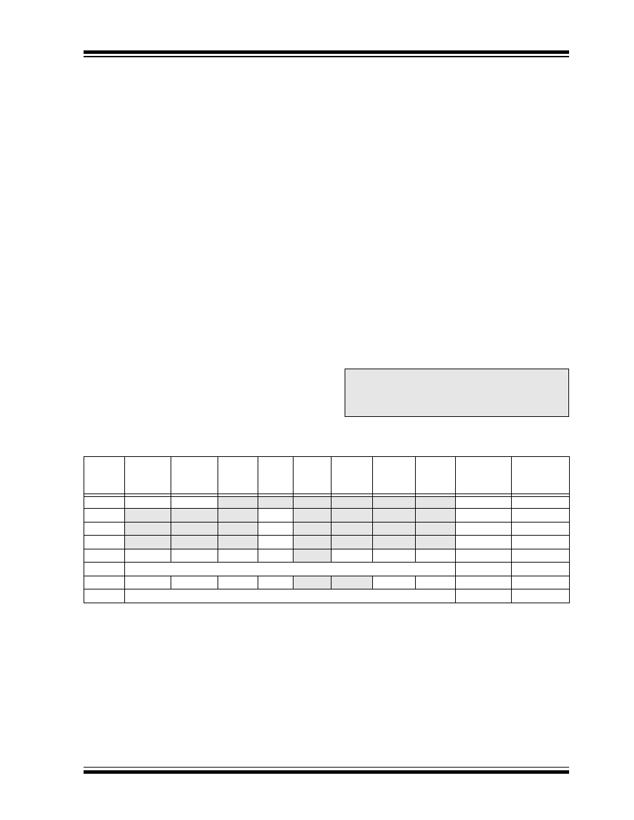
2002 Microchip Technology Inc.
Preliminary
DS41159B-page 191
PIC18FXX8
18.3
USART Synchronous Master
Mode
In Synchronous Master mode, the data is transmitted in
a half-duplex manner (i.e., transmission and reception
do not occur at the same time). When transmitting data,
the reception is inhibited and vice versa. Synchronous
mode is entered by setting bit SYNC (TXSTA register).
In addition, enable bit SPEN (RCSTA register) is set, in
order to configure the RC6/TX/CK and RC7/RX/DT I/O
pins to CK (clock) and DT (data) lines, respectively. The
Master mode indicates that the processor transmits the
master clock on the CK line. The Master mode is
entered by setting bit CSRC (TXSTA register).
18.3.1
USART SYNCHRONOUS MASTER
TRANSMISSION
The USART transmitter block diagram is shown in
Figure 18-1. The heart of the transmitter is the Transmit
(serial) Shift register (TSR). The shift register obtains
its data from the Read/Write Transmit Buffer register
(TXREG). The TXREG register is loaded with data in
software. The TSR register is not loaded until the last
bit has been transmitted from the previous load. As
soon as the last bit is transmitted, the TSR is loaded
with new data from the TXREG (if available). Once the
TXREG register transfers the data to the TSR register
(occurs in one T
CY
), the TXREG is empty and interrupt
bit TXIF (PIR registers) is set. The interrupt can be
enabled/disabled by setting/clearing enable bit TXIE
(PIE registers). Flag bit TXIF will be set, regardless of
the state of enable bit TXIE and cannot be cleared in
software. It will reset only when new data is loaded into
the TXREG register. While flag bit TXIF indicates the
status of the TXREG register, another bit TRMT
(TXSTA register) shows the status of the TSR register.
TRMT is a read only bit, which is set when the TSR is
empty. No interrupt logic is tied to this bit, so the user
has to poll this bit in order to determine if the TSR reg-
ister is empty. The TSR is not mapped in data memory,
so it is not available to the user.
Steps to follow when setting up a Synchronous Master
Transmission:
1.
Initialize the SPBRG register for the appropriate
baud rate (Section 18.1).
2.
Enable the synchronous master serial port by
setting bits SYNC, SPEN, and CSRC.
3.
If interrupts are desired, set enable bit TXIE.
4.
If 9-bit transmission is desired, set bit TX9.
5.
Enable the transmission by setting bit TXEN.
6.
If 9-bit transmission is selected, the ninth bit
should be loaded in bit TX9D.
7.
Start transmission by loading data to the TXREG
register.
TABLE 18-8:
REGISTERS ASSOCIATED WITH SYNCHRONOUS MASTER TRANSMISSION
Note:
TXIF is not cleared immediately upon load-
ing data into the transmit buffer TXREG. The
flag bit becomes valid in the second instruc-
tion cycle following the load instruction.
Name
Bit 7
Bit 6
Bit 5
Bit 4
Bit 3
Bit 2
Bit 1
Bit 0
Value on
POR, BOR
Value on
all other
RESETS
INTCON
GIE/GIEH
PEIE/GIEL
TMR0IE
INT0IE
RBIE
TMR0IF
INT0IF
RBIF
0000 000x
0000 000u
PIR1
PSPIF
ADIF
RCIF
TXIF
SSPIF
CCP1IF
TMR2IF
TMR1IF
0000 0000
0000 0000
PIE1
PSPIE
ADIE
RCIE
TXIE
SSPIE
CCP1IE
TMR2IE
TMR1IE
0000 0000
0000 0000
IPR1
PSPIP
ADIP
RCIP
TXIP
SSPIP
CCP1IP
TMR2IP
TMR1IP
0000 0000
0000 0000
RCSTA
SPEN
RX9
SREN
CREN
ADDEN
FERR
OERR
RX9D
0000 000x
0000 000x
TXREG
USART Transmit Register
0000 0000
0000 0000
TXSTA
CSRC
TX9
TXEN
SYNC
--
BRGH
TRMT
TX9D
0000 -010
0000 -010
SPBRG
Baud Rate Generator Register
0000 0000
0000 0000
Legend:
x
= unknown, - = unimplemented, read as '0'. Shaded cells are not used for Synchronous Master Transmission.
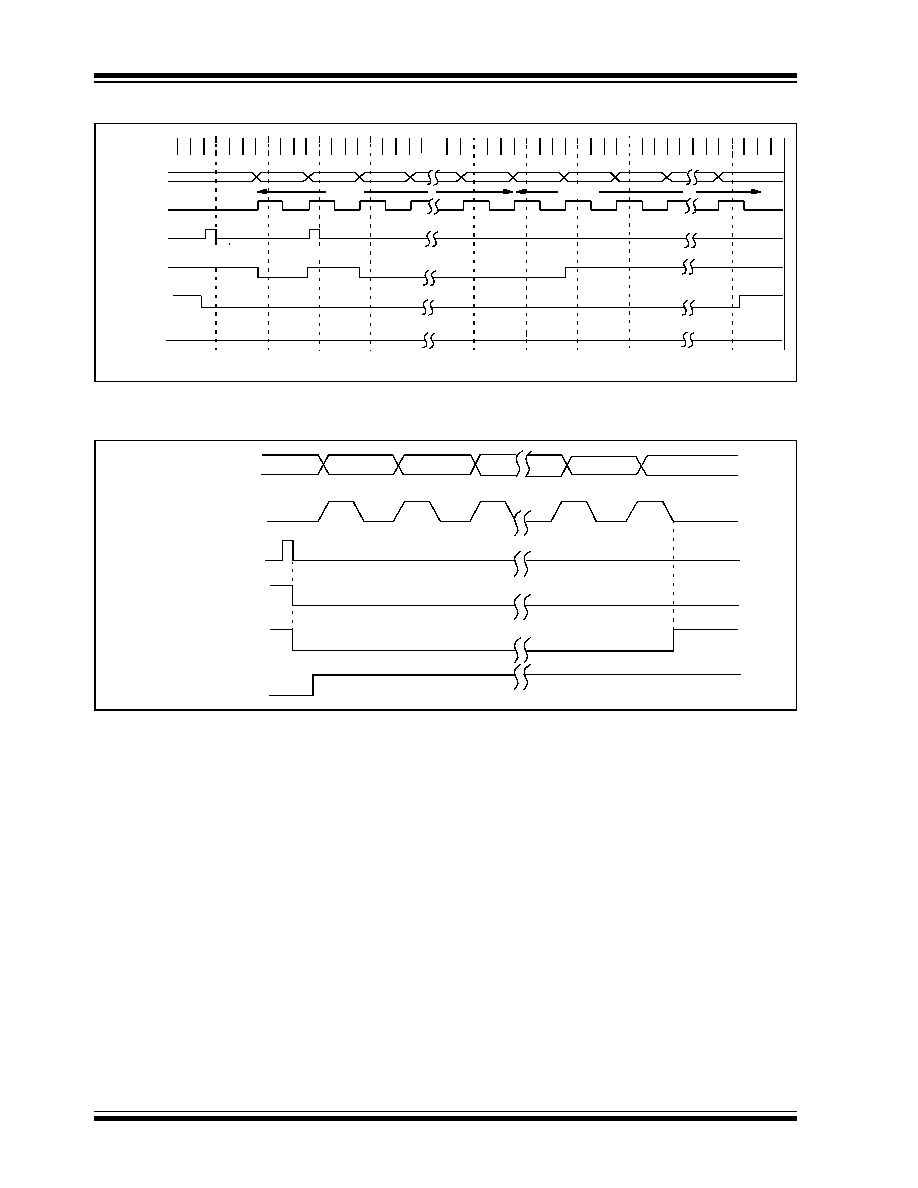
PIC18FXX8
DS41159B-page 192
Preliminary
2002 Microchip Technology Inc.
FIGURE 18-6:
SYNCHRONOUS TRANSMISSION
FIGURE 18-7:
SYNCHRONOUS TRANSMISSION (THROUGH TXEN)
bit 0
bit 1
bit 7
Word 1
Q1 Q2 Q3 Q4 Q1 Q2 Q3 Q4 Q1 Q2 Q3 Q4 Q1 Q2 Q3 Q4 Q1 Q2 Q3 Q4
Q4 Q1 Q2 Q3 Q4 Q1 Q2 Q3 Q4 Q1 Q2 Q3 Q4 Q1 Q2 Q3 Q4 Q1 Q2 Q3 Q4 Q1 Q2 Q3 Q4
bit 2
bit 0
bit 1
bit 7
RC7/RX/DT
RC6/TX/CK
Write to
TXREG Reg
TXIF bit
(Interrupt Flag)
TRMT
TXEN bit
'1'
'1'
Note: Sync Master mode; SPBRG = '0'; continuous transmission of two 8-bit words.
Word 2
TRMT bit
Write Word 1
Write Word 2
pin
pin
Q3
RC7/RX/DT pin
RC6/TX/CK pin
Write to
TXREG reg
TXIF bit
TRMT bit
bit0
bit1
bit2
bit6
bit7
TXEN bit
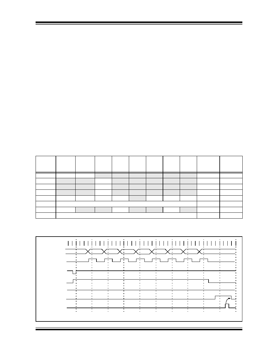
2002 Microchip Technology Inc.
Preliminary
DS41159B-page 193
PIC18FXX8
18.3.2
USART SYNCHRONOUS MASTER
RECEPTION
Once Synchronous Master mode is selected, reception
is enabled by setting either enable bit SREN (RCSTA
register), or enable bit CREN (RCSTA register). Data is
sampled on the RC7/RX/DT pin on the falling edge of
the clock. If enable bit SREN is set, only a single word
is received. If enable bit CREN is set, the reception is
continuous until CREN is cleared. If both bits are set,
then CREN takes precedence.
Steps to follow when setting up a Synchronous Master
Reception:
1.
Initialize the SPBRG register for the appropriate
baud rate (Section 18.1).
2.
Enable the synchronous master serial port by
setting bits SYNC, SPEN and CSRC.
3.
Ensure bits CREN and SREN are clear.
4.
If interrupts are desired, set enable bit RCIE.
5.
If 9-bit reception is desired, set bit RX9.
6.
If a single reception is required, set bit SREN.
For continuous reception, set bit CREN.
7.
Interrupt flag bit RCIF will be set when reception
is complete and an interrupt will be generated if
the enable bit RCIE was set.
8.
Read the RCSTA register to get the ninth bit (if
enabled) and determine if any error occurred
during reception.
9.
Read the 8-bit received data by reading the
RCREG register.
10. If any error occurred, clear the error by clearing
bit CREN.
TABLE 18-9:
REGISTERS ASSOCIATED WITH SYNCHRONOUS MASTER RECEPTION
FIGURE 18-8:
SYNCHRONOUS RECEPTION (MASTER MODE, SREN)
Name
Bit 7
Bit 6
Bit 5
Bit 4
Bit 3
Bit 2
Bit 1
Bit 0
Value on
POR, BOR
Value on
all other
RESETS
INTCON
GIE/GIEH PEIE/GIEL
TMR0IE
INT0IE
RBIE
TMR0IF
INT0IF
RBIF
0000 000x
0000 000u
PIR1
PSPIF
ADIF
RCIF
TXIF
SSPIF
CCP1IF
TMR2IF
TMR1IF
0000 0000
0000 0000
PIE1
PSPIE
ADIE
RCIE
TXIE
SSPIE
CCP1IE
TMR2IE
TMR1IE
0000 0000
0000 0000
IPR1
PSPIP
ADIP
RCIP
TXIP
SSPIP
CCP1IP
TMR2IP
TMR1IP
0000 0000
0000 0000
RCSTA
SPEN
RX9
SREN
CREN
ADDEN
FERR
OERR
RX9D
0000 000x
0000 000x
RCREG
USART Receive Register
0000 0000
0000 0000
TXSTA
CSRC
TX9
TXEN
SYNC
--
BRGH
TRMT
TX9D
0000 -010
0000 -010
SPBRG
Baud Rate Generator Register
0000 0000
0000 0000
Legend:
x
= unknown, - = unimplemented, read as '0'. Shaded cells are not used for Synchronous Master Reception.
CREN bit
RC7/RX/DT pin
RC6/TX/CK pin
Write to
bit SREN
SREN bit
RCIF bit
(Interrupt)
Read
RXREG
Note: Timing diagram demonstrates Sync Master mode with bit SREN = '1' and bit BRGH = '0'.
Q3 Q4 Q1 Q2 Q3 Q4 Q1 Q2 Q3 Q4
Q2
Q1 Q2 Q3 Q4 Q1 Q2 Q3 Q4 Q1 Q2 Q3 Q4 Q1 Q2 Q3 Q4 Q1 Q2 Q3 Q4 Q1 Q2 Q3 Q4 Q1 Q2 Q3 Q4
'0'
bit0
bit1
bit2
bit3
bit4
bit5
bit6
bit7
'0'
Q1 Q2 Q3 Q4

PIC18FXX8
DS41159B-page 194
Preliminary
2002 Microchip Technology Inc.
18.4
USART Synchronous Slave Mode
Synchronous Slave mode differs from the Master
mode, in that the shift clock is supplied externally at the
RC6/TX/CK pin (instead of being supplied internally in
Master mode). This allows the device to transfer or
receive data while in SLEEP mode. Slave mode is
entered by clearing bit CSRC (TXSTA register).
18.4.1
USART SYNCHRONOUS SLAVE
TRANSMIT
The operation of the Synchronous Master and Slave
modes are identical, except in the case of the SLEEP
mode.
If two words are written to the TXREG and then the
SLEEP
instruction is executed, the following will occur:
a)
The first word will immediately transfer to the
TSR register and transmit.
b)
The second word will remain in TXREG register.
c)
Flag bit TXIF will not be set.
d)
When the first word has been shifted out of TSR,
the TXREG register will transfer the second
word to the TSR and flag bit TXIF will be set.
e)
If enable bit TXIE is set, the interrupt will wake
the chip from SLEEP. If the global interrupt is
enabled, the program will branch to the interrupt
vector.
Steps to follow when setting up a Synchronous Slave
Transmission:
1.
Enable the synchronous slave serial port by set-
ting bits SYNC and SPEN and clearing bit
CSRC.
2.
Clear bits CREN and SREN.
3.
If interrupts are desired, set enable bit TXIE.
4.
If 9-bit transmission is desired, set bit TX9.
5.
Enable the transmission by setting enable bit
TXEN.
6.
If 9-bit transmission is selected, the ninth bit
should be loaded in bit TX9D.
7.
Start transmission by loading data to the TXREG
register.
18.4.2
USART SYNCHRONOUS SLAVE
RECEPTION
The operation of the Synchronous Master and Slave
modes is identical, except in the case of the SLEEP
mode and bit SREN, which is a "don't care" in Slave
mode.
If receive is enabled by setting bit CREN prior to the
SLEEP
instruction, then a word may be received during
SLEEP. On completely receiving the word, the RSR
register will transfer the data to the RCREG register,
and if enable bit RCIE bit is set, the interrupt generated
will wake the chip from SLEEP. If the global interrupt is
enabled, the program will branch to the interrupt vector.
Steps to follow when setting up a Synchronous Slave
Reception:
1.
Enable the synchronous master serial port by
setting bits SYNC and SPEN and clearing bit
CSRC.
2.
If interrupts are desired, set enable bit RCIE.
3.
If 9-bit reception is desired, set bit RX9.
4.
To enable reception, set enable bit CREN.
5.
Flag bit RCIF will be set when reception is com-
plete. An interrupt will be generated if enable bit
RCIE was set.
6.
Read the RCSTA register to get the ninth bit (if
enabled) and determine if any error occurred
during reception.
7.
Read the 8-bit received data by reading the
RCREG register.
8.
If any error occurred, clear the error by clearing
bit CREN.
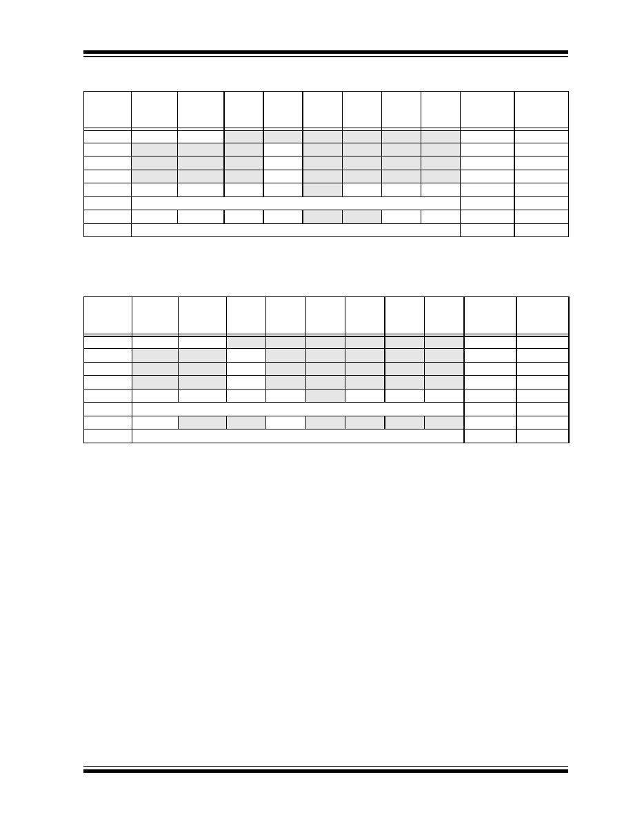
2002 Microchip Technology Inc.
Preliminary
DS41159B-page 195
PIC18FXX8
TABLE 18-10: REGISTERS ASSOCIATED WITH SYNCHRONOUS SLAVE TRANSMISSION
TABLE 18-11: REGISTERS ASSOCIATED WITH SYNCHRONOUS SLAVE RECEPTION
Name
Bit 7
Bit 6
Bit 5
Bit 4
Bit 3
Bit 2
Bit 1
Bit 0
Value on
POR, BOR
Value on
all other
RESETS
INTCON
GIE/GIEH
PEIE/GIEL TMR0IE
INT0IE
RBIE
TMR0IF
INT0IF
RBIF
0000 000x
0000 000u
PIR1
PSPIF
ADIF
RCIF
TXIF
SSPIF
CCP1IF
TMR2IF
TMR1IF
0000 0000
0000 0000
PIE1
PSPIE
ADIE
RCIE
TXIE
SSPIE
CCP1IE
TMR2IE
TMR1IE
0000 0000
0000 0000
IPR1
PSPIP
ADIP
RCIP
TXIP
SSPIP
CCP1IP
TMR2IP
TMR1IP
0000 0000
0000 0000
RCSTA
SPEN
RX9
SREN
CREN
ADDEN
FERR
OERR
RX9D
0000 000x
0000 000x
TXREG
USART Transmit Register
0000 0000
0000 0000
TXSTA
CSRC
TX9
TXEN
SYNC
--
BRGH
TRMT
TX9D
0000 -010
0000 -010
SPBRG
Baud Rate Generator Register
0000 0000
0000 0000
Legend:
x
= unknown, - = unimplemented, read as '0'. Shaded cells are not used for Synchronous Slave Transmission.
Name
Bit 7
Bit 6
Bit 5
Bit 4
Bit 3
Bit 2
Bit 1
Bit 0
Value on
POR,
BOR
Value on all
other
RESETS
INTCON
GIE/GIEH
PEIE/GIEL
TMR0IE
INT0IE
RBIE
TMR0IF
INT0IF
RBIF
0000 000x
0000 000u
PIR1
PSPIF
ADIF
RCIF
TXIF
SSPIF
CCP1IF
TMR2IF
TMR1IF
0000 0000
0000 0000
PIE1
PSPIE
ADIE
RCIE
TXIE
SSPIE
CCP1IE
TMR2IE
TMR1IE
0000 0000
0000 0000
IPR1
PSPIP
ADIP
RCIP
TXIP
SSPIP
CCP1IP
TMR2IP
TMR1IP
0000 0000
0000 0000
RCSTA
SPEN
RX9
SREN
CREN
ADDEN
FERR
OERR
RX9D
0000 000x
0000 000x
RCREG
USART Receive Register
0000 0000
0000 0000
TXSTA
CSRC
TX9
TXEN
SYNC
--
BRGH
TRMT
TX9D
0000 -010
0000 -010
SPBRG
Baud Rate Generator Register
0000 0000
0000 0000
Legend:
x
= unknown, - = unimplemented, read as '0'. Shaded cells are not used for Synchronous Slave Reception.

PIC18FXX8
DS41159B-page 196
Preliminary
2002 Microchip Technology Inc.
NOTES:

2002 Microchip Technology Inc.
Preliminary
DS41159B-page 197
PIC18FXX8
19.0
CAN MODULE
19.1
Overview
The Controller Area Network (CAN) module is a serial
interface, useful for communicating with other peripher-
als or microcontroller devices. This interface/protocol
was designed to allow communications within noisy
environments.
The CAN module is a communication controller, imple-
menting the CAN 2.0 A/B protocol as defined in the
BOSCH specification. The module will support CAN
1.2, CAN 2.0A, CAN2.0B Passive, and CAN 2.0B
Active versions of the protocol. The module implemen-
tation is a full CAN system. The CAN specification is
not covered within this data sheet. The reader may
refer to the BOSCH CAN specification for further
details.
The module features are as follows:
� Implementation of the CAN protocol CAN1.2,
CAN2.0A and CAN2.0B
� Standard and extended data frames
� 0 - 8 bytes data length
� Programmable bit rate up to 1 Mbit/sec
� Support for remote frames
� Double-buffered receiver with two prioritized
received message storage buffers
� 6 full (standard/extended identifier) acceptance
filters, 2 associated with the high priority receive
buffer, and 4 associated with the low priority
receive buffer
� 2 full acceptance filter masks, one each
associated with the high and low priority receive
buffers
� Three transmit buffers with application specified
prioritization and abort capability
� Programmable wake-up functionality with
integrated low pass filter
� Programmable Loopback mode supports self-test
operation
� Signaling via interrupt capabilities for all CAN
receiver and transmitter error states
� Programmable clock source
� Programmable link to timer module for
time-stamping and network synchronization
� Low power SLEEP mode
19.1.1
OVERVIEW OF THE MODULE
The CAN bus module consists of a protocol engine and
message buffering and control. The CAN protocol
engine handles all functions for receiving and transmit-
ting messages on the CAN bus. Messages are trans-
mitted by first loading the appropriate data registers.
Status and errors can be checked by reading the
appropriate registers. Any message detected on the
CAN bus is checked for errors and then matched
against filters to see if it should be received and stored
in one of the 2 receive registers.
The CAN Module supports the following frame types:
� Standard Data Frame
� Extended Data Frame
� Remote Frame
� Error Frame
� Overload Frame Reception
� Interframe Space
CAN module uses RB3/CANRX and RB2/CANTX/INT2
pins to interface with CAN bus. In order to configure
CANRX and CANTX as CAN interface:
� bit TRISB<3> must be set;
� bit TRISB<2> must be cleared.
19.1.2
TRANSMIT/RECEIVE BUFFERS
The PIC18FXX8 has three transmit and two receive buff-
ers, two acceptance masks (one for each receive
buffer), and a total of six acceptance filters. Figure 19-1
is a block diagram of these buffers and their connection
to the protocol engine.
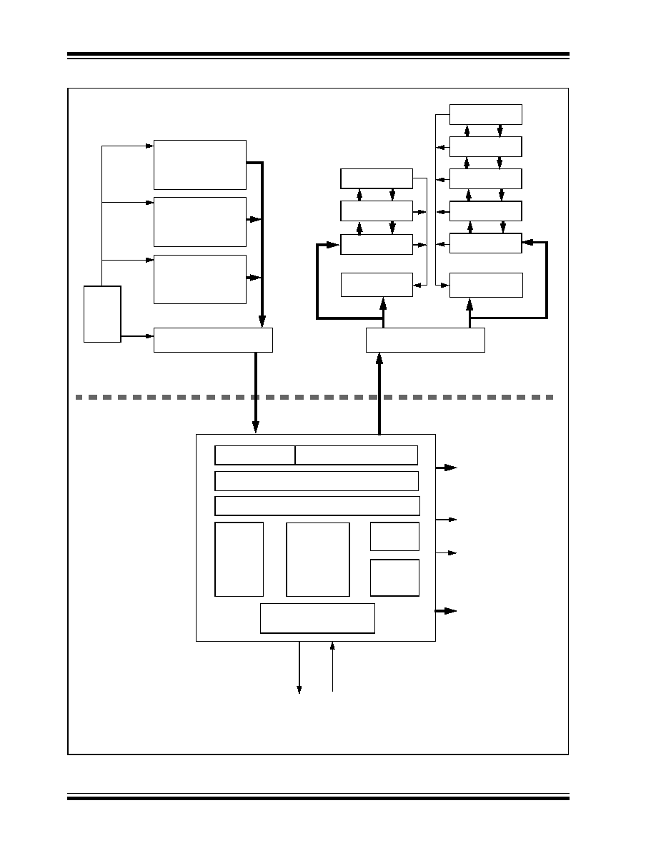
PIC18FXX8
DS41159B-page 198
Preliminary
2002 Microchip Technology Inc.
FIGURE 19-1:
CAN BUFFERS AND PROTOCOL ENGINE BLOCK DIAGRAM
Acceptance Mask
RXM0
Acceptance Filter
RXF0
Acceptance Filter
RXF1
Message
Queue
Control
Transmit Byte Sequencer
TXREQ
TXB0
TXABT
TXLARB
TXERR
TXBUFF
MESSAGE
Receive Shift
Receive
Error
Transmit
Error
RXERRCNT
TXERRCNT
Err-Pas
Bus-Off
Counter
Counter
Transmit
Logic
Bit Timing
Logic
TX
RX
Bit Timing
Generator
PROTOCOL
ENGINE
BUFFERS
Transmit Shift
Protocol
FSM
Comparator
CRC Register
TXREQ
TXB1
TXABT
TXLARB
TXERR
TXBUFF
MESSAGE
TXREQ
TXB2
TXABT
TXLARB
TXERR
TXBUFF
MESSAGE
Message Assembly Buffer
Acceptance Filter
RXM2
Acceptance Filter
RXF3
Acceptance Filter
RXF4
Acceptance Filter
RXF5
Acceptance Mask
RXM1
RXB0
RXB1
Accept
Accept
Message
Request
Data and
Identifier
Data and
Identifier
Identifier
Identifier

2002 Microchip Technology Inc.
Preliminary
DS41159B-page 199
PIC18FXX8
19.2
CAN Module Registers
There are many control and data registers associated
with the CAN module. For convenience, their
descriptions have been grouped into the following
sections:
� Control and Status Registers
� Transmit Buffer Registers (Data and Control)
� Receive Buffer Registers (Data and Control)
� Baud Rate Control Registers
� I/O Control Register
� Interrupt Status and Control Registers
19.2.1
CAN CONTROL AND STATUS
REGISTERS
The registers described in this section control the over-
all operation of the CAN module and show its
operational status.
REGISTER 19-1:
CANCON � CAN CONTROL REGISTER
Note:
Not all CAN registers are available in the
access bank.
R/W-1
R/W-0
R/W-0
R/W-0
R/W-0
R/W-0
R/W-0
U-0
REQOP2
REQOP1
REQOP0
ABAT
WIN2
WIN1
WIN0
--
bit 7
bit 0
bit 7-5
REQOP2:REQOP0: Request CAN Operation Mode bits
1xx
= Request Configuration mode
011
= Request Listen Only mode
010
= Request Loopback mode
001
= Request Disable mode
000
= Request Normal mode
bit 4
ABAT: Abort All Pending Transmissions bit
1
= Abort all pending transmissions (in all transmit buffers)
0
= Transmissions proceeding as normal
bit 3-1
WIN2:WIN0: Window Address bits
This selects which of the CAN buffers to switch into the access bank area. This allows access
to the buffer registers from any data memory bank. After a frame has caused an interrupt, the
ICODE3:ICODE0 bits can be copied to the WIN3:WIN0 bits to select the correct buffer. See
Example 19-1 for code example.
111
= Receive Buffer 0
110
= Receive Buffer 0
101
= Receive Buffer 1
100
= Transmit Buffer 0
011
= Transmit Buffer 1
010
= Transmit Buffer 2
001
= Receive Buffer 0
000
= Receive Buffer 0
bit 0
Unimplemented: Read as `0'
Legend:
R = Readable bit
W = Writable bit
U = Unimplemented bit, read as `0'
- n = Value at POR
'1' = Bit is set
'0' = Bit is cleared
x = Bit is unknown

PIC18FXX8
DS41159B-page 200
Preliminary
2002 Microchip Technology Inc.
REGISTER 19-2:
CANSTAT � CAN STATUS REGISTER
R-1
R-0
R-0
U-0
R-0
R-0
R-0
U-0
OPMODE2 OPMODE1 OPMODE0
--
ICODE2
ICODE1
ICODE0
--
bit 7
bit 0
bit 7-5
OPMODE2:OPMODE0: Operation Mode Status bits
111
= Reserved
110
= Reserved
101
= Reserved
100
= Configuration mode
011
= Listen Only mode
010
= Loopback mode
001
= Disable mode
000
= Normal mode
Note:
Before the device goes into SLEEP mode, select Disable mode.
bit 4
Unimplemented: Read as '0'
bit 3-1
ICODE2:ICODE0: Interrupt Code bits
When an interrupt occurs, a prioritized coded interrupt value will be present in the
ICODE3:ICODE0 bits. These codes indicate the source of the interrupt. The ICODE3:ICODE0
bits can be copied to the WIN3:WIN0 bits to select the correct buffer to map into the Access
Bank area. See Example 19-1 for code example.
111
= Wake-up on Interrupt
110
= RXB0 Interrupt
101
= RXB1 Interrupt
100
= TXB0 Interrupt
011
= TXB1 Interrupt
010
= TXB2 Interrupt
001
= Error Interrupt
000
= No Interrupt
bit 0
Unimplemented: Read as '0'
Legend:
R = Readable bit
W = Writable bit
U = Unimplemented bit, read as `0'
- n = Value at POR
'1' = Bit is set
'0' = Bit is cleared
x = Bit is unknown

2002 Microchip Technology Inc.
Preliminary
DS41159B-page 201
PIC18FXX8
EXAMPLE 19-1:
WIN AND ICODE BITS USAGE IN INTERRUPT SERVICE ROUTINE TO ACCESS
TX/RX BUFFERS
; Save application required context.
; Poll interrupt flags and determine source of interrupt
; This was found to be CAN interrupt
; TempCANCON and TempCANSTAT are variables defined in Access Bank low
MOVFF
CANCON, TempCANCON
; Save CANCON.WIN bits
; This is required to prevent CANCON
; from corrupting CAN buffer access
; in-progress while this interrupt
; occurred
MOVFF
CANSTAT, TempCANSTAT
; Save CANSTAT register
; This is required to make sure that
; we use same CANSTAT value rather
; than one changed by another CAN
; interrupt.
MOVF
TempCANSTAT, W
; Retrieve ICODE bits
ANDLW
b'00001110'
ADDWF
PCL, F
; Perform computed GOTO
; to corresponding interrupt cause
BRA
NoInterrupt
; 000 = No interrupt
BRA
ErrorInterrupt
; 001 = Error interrupt
BRA
TXB2Interrupt
; 010 = TXB2 interrupt
BRA
TXB1Interrupt
; 011 = TXB1 interrupt
BRA
TXB0Interrupt
; 100 = TXB0 interrupt
BRA
RXB1Interrupt
; 101 = RXB1 interrupt
BRA
RXB0Interrupt
; 110 = RXB0 interrupt
; 111 = Wake-up on interrupt
WakeupInterrupt
BCF
PIR3, WAKIF
; Clear the interrupt flag
;
; User code to handle wake-up procedure
;
;
; Continue checking for other interrupt source or return from here
...
NoInterrupt
...
; PC should never vector here. User may
; place a trap such as infinite loop or pin/port
; indication to catch this error.
ErrorInterrupt
BCF
PIR3, ERRIF
; Clear the interrupt flag
...
; Handle error.
RETFIE
TXB2Interrupt
BCF
PIR3, TXB2IF
; Clear the interrupt flag
GOTO
AccessBuffer
TXB1Interrupt
BCF
PIR3, TXB1IF
; Clear the interrupt flag
GOTO
AccessBuffer
TXB0Interrupt
BCF
PIR3, TXB0IF
; Clear the interrupt flag
GOTO
AccessBuffer
RXB1Interrupt
BCF
PIR3, RXB1IF
; Clear the interrupt flag
GOTO
Accessbuffer

PIC18FXX8
DS41159B-page 202
Preliminary
2002 Microchip Technology Inc.
EXAMPLE 19-1:
WIN AND ICODE BITS USAGE IN INTERRUPT SERVICE ROUTINE TO ACCESS
TX/RX BUFFERS (CONTINUED)
RXB0Interrupt
BCF
PIR3, RXB0IF
; Clear the interrupt flag
GOTO
AccessBuffer
AccessBuffer
; This is either TX or RX interrupt
; Copy CANCON.ICODE bits to CANSTAT.WIN bits
MOVF
TempCANCON, W
; Clear CANCON.WIN bits before copying
; new ones.
ANDLW
b'11110001'
; Use previously saved CANCON value to
; make sure same value.
MOVWF
TempCANCON
; Copy masked value back to TempCANCON
MOVF
TempCANSTAT, W
; Retrieve ICODE bits
ANDLW
b'00001110'
; Use previously saved CANSTAT value
; to make sure same value.
IORWF
TempCANCON
; Copy ICODE bits to WIN bits.
MOVFF
TempCANCON, CANCON
; Copy the result to actual CANCON
; Access current buffer...
; User code
; Restore CANCON.WIN bits
MOVF
CANCON, W
; Preserve current non WIN bits
ANDLW
b'11110001'
IORWF
TempCANCON
; Restore original WIN bits
; Do not need to restore CANSTAT - it is read-only register.
; Return from interrupt or check for another module interrupt source

2002 Microchip Technology Inc.
Preliminary
DS41159B-page 203
PIC18FXX8
REGISTER 19-3:
COMSTAT � COMMUNICATION STATUS REGISTER
R/C-0
R/C-0
R-0
R-0
R-0
R-0
R-0
R-0
RXB0OVFL RXB1OVFL
TXBO
TXBP
RXBP
TXWARN RXWARN
EWARN
bit 7
bit 0
bit 7
RXB0OVFL: Receive Buffer 0 Overflow bit
1
= Receive Buffer 0 overflowed
0
= Receive Buffer 0 has not overflowed
bit 6
RXB1OVFL: Receive Buffer 1 Overflow bit
1
= Receive Buffer 1 overflowed
0
= Receive Buffer 1 has not overflowed
bit 5
TXBO: Transmitter Bus-Off bit
1
= Transmit Error Counter > 255
0
= Transmit Error Counter
255
bit 4
TXBP: Transmitter Bus Passive bit
1
= Transmission Error Counter > 127
0
= Transmission Error Counter
127
bit 3
RXBP: Receiver Bus Passive bit
1
= Receive Error Counter > 127
0
= Receive Error Counter
127
bit 2
TXWARN: Transmitter Warning bit
1
= 127
Transmit Error Counter > 95
0
= Transmit Error Counter
95
bit 1
RXWARN: Receiver Warning bit
1
= 127
Receive Error Counter > 95
0
= Receive Error Counter
95
bit 0
EWARN: Error Warning bit
This bit is a flag of the RXWARN and TXWARN bits
1
= The RXWARN or the TXWARN bits are set
0
= Neither the RXWARN or the TXWARN bits are set
Legend:
R = Readable bit
W = Writable bit
U = Unimplemented bit, read as `0'
- n = Value at POR
'1' = Bit is set
'0' = Bit is cleared
x = Bit is unknown

PIC18FXX8
DS41159B-page 204
Preliminary
2002 Microchip Technology Inc.
19.2.2
CAN TRANSMIT BUFFER
REGISTERS
This section describes the CAN Transmit Buffer
registers and their associated control registers.
REGISTER 19-4:
TXBnCON � TRANSMIT BUFFER n CONTROL REGISTERS
U-0
R-0
R-0
R-0
R/W-0
U-0
R/W-0
R/W-0
--
TXABT
TXLARB
TXERR
TXREQ
--
TXPRI1
TXPRI0
bit 7
bit 0
bit 7
Unimplemented: Read as '0'
bit 6
TXABT: Transmission Aborted Status bit
1
= Message was aborted
0
= Message was not aborted
bit 5
TXLARB: Transmission Lost Arbitration Status bit
1
= Message lost arbitration while being sent
0
= Message did not lose arbitration while being sent
bit 4
TXERR: Transmission Error Detected Status bit
1
= A bus error occurred while the message was being sent
0
= A bus error did not occur while the message was being sent
bit 3
TXREQ: Transmit Request Status bit
1
= Requests sending a message. Clears the TXABT, TXLARB, and TXERR bits.
0
= Automatically cleared when the message is successfully sent
Note:
Clearing this bit in software while the bit is set, will request a message abort.
bit 2
Unimplemented: Read as '0'
bit 1-0
TXPRI1:TXPRI0: Transmit Priority bits
11
= Priority Level 3 (Highest Priority)
10
= Priority Level 2
01
= Priority Level 1
00
= Priority Level 0 (Lowest Priority)
Note:
These bits set the order in which Transmit buffer will be transferred. They do not
alter CAN message identifier.
Legend:
R = Readable bit
W = Writable bit
U = Unimplemented bit, read as `0'
- n = Value at POR
'1' = Bit is set
'0' = Bit is cleared
x = Bit is unknown

2002 Microchip Technology Inc.
Preliminary
DS41159B-page 205
PIC18FXX8
REGISTER 19-5:
TXBnSIDH: TRANSMIT BUFFER n STANDARD IDENTIFIER, HIGH BYTE
REGISTER 19-6:
TXBnSIDL � TRANSMIT BUFFER n STANDARD IDENTIFIER, LOW BYTE
REGISTER 19-7:
TXBnEIDH � TRANSMIT BUFFER n EXTENDED IDENTIFIER, HIGH BYTE
R/W-x
R/W-x
R/W-x
R/W-x
R/W-x
R/W-x
R/W-x
R/W-x
SID10
SID9
SID8
SID7
SID6
SID5
SID4
SID3
bit 7
bit 0
bit 7-0
SID10:SID3: Standard Identifier bits, if EXIDE = 0 (TXBnSID Register)
Extended Identifier bits EID28:EID21, if EXIDE = 1
Legend:
R = Readable bit
W = Writable bit
U = Unimplemented bit, read as `0'
- n = Value at POR
'1' = Bit is set
'0' = Bit is cleared
x = Bit is unknown
R/W-x
R/W-x
R/W-x
R/W-x
R/W-x
R/W-x
R/W-x
R/W-x
SID2
SID1
SID0
--
EXIDE
--
EID17
EID16
bit 7
bit 0
bit 7-5
SID2:SID0: Standard Identifier bits, if EXIDE = 0
Extended Identifier bits EID20:EID18, if EXIDE = 1
bit 4
Unimplemented: Read as '0'
bit 3
EXIDE: Extended Identifier Enable bit
1
= Message will transmit Extended ID, SID10:SID0 becomes EID28:EID18
0
= Message will transmit Standard ID, EID17:EID0 are ignored
bit 2
Unimplemented: Read as '0'
bit 1-0
EID17:EID16: Extended Identifier bits
Legend:
R = Readable bit
W = Writable bit
U = Unimplemented bit, read as `0'
- n = Value at POR
'1' = Bit is set
'0' = Bit is cleared
x = Bit is unknown
R/W-x
R/W-x
R/W-x
R/W-x
R/W-x
R/W-x
R/W-x
R/W-x
EID15
EID14
EID13
EID12
EID11
EID10
EID9
EID8
bit 7
bit 0
bit 7-0
EID15:EID8: Extended Identifier bits
Legend:
R = Readable bit
W = Writable bit
U = Unimplemented bit, read as `0'
- n = Value at POR
'1' = Bit is set
'0' = Bit is cleared
x = Bit is unknown

PIC18FXX8
DS41159B-page 206
Preliminary
2002 Microchip Technology Inc.
REGISTER 19-8:
TXBnEIDL � TRANSMIT BUFFER n EXTENDED IDENTIFIER, LOW BYTE
REGISTER 19-9:
TXBnDm � TRANSMIT BUFFER n DATA FIELD BYTE m REGISTERS
R/W-x
R/W-x
R/W-x
R/W-x
R/W-x
R/W-x
R/W-x
R/W-x
EID7
EID6
EID5
EID4
EID3
EID2
EID1
EID0
bit 7
bit 0
bit 7-0
EID7:EID0: Extended Identifier bits
Legend:
R = Readable bit
W = Writable bit
U = Unimplemented bit, read as `0'
- n = Value at POR
'1' = Bit is set
'0' = Bit is cleared
x = Bit is unknown
R/W-x
R/W-x
R/W-x
R/W-x
R/W-x
R/W-x
R/W-x
R/W-x
TXBnDm7 TXBnDm6 TXBnDm5 TXBnDm4 TXBnDm3 TXBnDm2 TXBnDm1 TXBnDm0
bit 7
bit 0
bit 7-0
TXBnDm7:TXBnDm0: Transmit Buffer n Data Field Byte m bits (where 0
n<3 and 0<m<8)
Each Transmit Buffer has an array of registers. For example, Transmit buffer 0 has 7 registers:
TXB0D0 to TXB0D7.
Legend:
R = Readable bit
W = Writable bit
U = Unimplemented bit, read as `0'
- n = Value at POR
'1' = Bit is set
'0' = Bit is cleared
x = Bit is unknown

2002 Microchip Technology Inc.
Preliminary
DS41159B-page 207
PIC18FXX8
REGISTER 19-10: TXBnDLC � TRANSMIT BUFFER n DATA LENGTH CODE REGISTERS
REGISTER 19-11: TXERRCNT � TRANSMIT ERROR COUNT REGISTER
U-0
R/W-x
U-0
U-0
R/W-x
R/W-x
R/W-x
R/W-x
--
TXRTR
--
--
DLC3
DLC2
DLC1
DLC0
bit 7
bit 0
bit 7
Unimplemented: Read as '0'
bit 6
TXRTR: Transmission Frame Remote Transmission Request bit
1
= Transmitted message will have TXRTR bit set
0
= Transmitted message will have TXRTR bit cleared
bit 5-4
Unimplemented: Read as '0'
bit 3-0
DLC3:DLC0: Data Length Code bits
1111
= Reserved
1110
= Reserved
1101
= Reserved
1100
= Reserved
1011
= Reserved
1010
= Reserved
1001
= Reserved
1000
= Data Length = 8 bytes
0111
= Data Length = 7 bytes
0110
= Data Length = 6 bytes
0101
= Data Length = 5 bytes
0100
= Data Length = 4 bytes
0011
= Data Length = 3 bytes
0010
= Data Length = 2 bytes
0001
= Data Length = 1 bytes
0000
= Data Length = 0 bytes
Legend:
R = Readable bit
W = Writable bit
U = Unimplemented bit, read as `0'
- n = Value at POR
'1' = Bit is set
'0' = Bit is cleared
x = Bit is unknown
R-0
R-0
R-0
R-0
R-0
R-0
R-0
R-0
TEC7
TEC6
TEC5
TEC4
TEC3
TEC2
TEC1
TEC0
bit 7
bit 0
bit 7-0
TEC7:TEC0: Transmit Error Counter bits
This register contains a value which is derived from the rate at which errors occur. When the
error count overflows, the bus-off state occurs. When the bus has 128 occurrences of 11
consecutive recessive bits, the counter value is cleared.
Legend:
R = Readable bit
W = Writable bit
U = Unimplemented bit, read as `0'
- n = Value at POR
'1' = Bit is set
'0' = Bit is cleared
x = Bit is unknown

PIC18FXX8
DS41159B-page 208
Preliminary
2002 Microchip Technology Inc.
19.2.3
CAN RECEIVE BUFFER
REGISTERS
This section shows the Receive Buffer registers with
their associated control registers.
REGISTER 19-12: RXB0CON � RECEIVE BUFFER 0 CONTROL REGISTER
R/C-0
R/W-0
R/W-0
U-0
R-0
R/W-0
R-0
R/W-0
RXFUL
(1)
RXM1
(1)
RXM0
(1)
--
RXRTRRO RXB0DBEN
JTOFF
FILHIT0
bit 7
bit 0
bit 7
RXFUL: Receive Full Status bit
(1)
1
= Receive buffer contains a received message
0
= Receive buffer is open to receive a new message
Note:
This bit is set by the CAN module and must be cleared by software after the buffer
is read.
bit 6-5
RXM1:RXM0: Receive Buffer Mode bits
(1)
11
= Receive all messages (including those with errors)
10
= Receive only valid messages with extended identifier
01
= Receive only valid messages with standard identifier
00
= Receive all valid messages
bit 4
Unimplemented: Read as '0'
bit 3
RXRTRRO: Receive Remote Transfer Request Read Only bit
1
= Remote transfer request
0
= No remote transfer request
bit 2
RXB0DBEN: Receive Buffer 0 Double Buffer Enable bit
1
= Receive Buffer 0 overflow will write to Receive Buffer 1
0
= No Receive Buffer 0 overflow to Receive Buffer 1
bit 1
JTOFF: Jump Table Offset bit (read only copy of RXB0DBEN)
1
= Allows Jump Table offset between 6 and 7
0
= Allows Jump Table offset between 1 and 0
Note:
This bit allows same filter jump table for both RXB0CON and RXB1CON.
bit 0
FILHIT0: Filter Hit bit
This bit indicates which acceptance filter enabled the message reception into Receive Buffer 0
1
= Acceptance Filter 1 (RXF1)
0
= Acceptance Filter 0 (RXF0)
Note
1: Bits RXFUL, RXM1 and RXM0 of RXB0CON are not mirrored in RXB1CON.
Legend:
R = Readable bit
W = Writable bit
U = Unimplemented bit, read as `0'
- n = Value at POR
'1' = Bit is set
'0' = Bit is cleared
x = Bit is unknown

2002 Microchip Technology Inc.
Preliminary
DS41159B-page 209
PIC18FXX8
REGISTER 19-13: RXB1CON � RECEIVE BUFFER 1 CONTROL REGISTER
REGISTER 19-14: RXBnSIDH � RECEIVE BUFFER n STANDARD IDENTIFIER, HIGH BYTE
REGISTER
R/C-0
R/W-0
R/W-0
U-0
R-0
R-0
R-0
R-0
RXFUL
(1)
RXM1
(1)
RXM0
(1)
--
RXRTRRO
FILHIT2
FILHIT1
FILHIT0
bit 7
bit 0
bit 7
RXFUL: Receive Full Status bit
(1)
1
= Receive buffer contains a received message
0
= Receive buffer is open to receive a new message
Note:
This bit is set by the CAN module and should be cleared by software after the buffer
is read.
bit 6-5
RXM1:RXM0: Receive Buffer Mode bits
(1)
11
= Receive all messages (including those with errors)
10
= Receive only valid messages with extended identifier
01
= Receive only valid messages with standard identifier
00
= Receive all valid messages
bit 4
Unimplemented: Read as '0'
bit 3
RXRTRRO: Receive Remote Transfer Request bit (read only)
1
= Remote transfer request
0
= No remote transfer request
bit 2-0
FILHIT2:FILHIT0: Filter Hit bits
These bits indicate which acceptance filter enabled the last message reception into Receive
Buffer 1
111
= Reserved
110
= Reserved
101
= Acceptance Filter 5 (RXF5)
100
= Acceptance Filter 4 (RXF4)
011
= Acceptance Filter 3 (RXF3)
010
= Acceptance Filter 2 (RXF2)
001
= Acceptance Filter 1 (RXF1) only possible when RXB0DBEN bit is set
000
= Acceptance Filter 0 (RXF0) only possible when RXB0DBEN bit is set
Note
1: Bits RXFUL, RXM1 and RXM0 of RXB1CON are not mirrored in RXB0CON.
Legend:
R = Readable bit
W = Writable bit
U = Unimplemented bit, read as `0'
- n = Value at POR
'1' = Bit is set
'0' = Bit is cleared
x = Bit is unknown
R/W-x
R/W-x
R/W-x
R/W-x
R/W-x
R/W-x
R/W-x
R/W-x
SID10
SID9
SID8
SID7
SID6
SID5
SID4
SID3
bit 7
bit 0
bit 7-0
SID10:SID3: Standard Identifier bits, if EXID = 0 (RXBnSIDL Register)
Extended Identifier bits EID28:EID21, if EXID = 1
Legend:
R = Readable bit
W = Writable bit
U = Unimplemented bit, read as `0'
- n = Value at POR
'1' = Bit is set
'0' = Bit is cleared
x = Bit is unknown

PIC18FXX8
DS41159B-page 210
Preliminary
2002 Microchip Technology Inc.
REGISTER 19-15: RXBnSIDL � RECEIVE BUFFER n STANDARD IDENTIFIER, LOW BYTE
REGISTER 19-16: RXBnEIDH � RECEIVE BUFFER n EXTENDED IDENTIFIER, HIGH BYTE
REGISTER 19-17: RXBnEIDL � RECEIVE BUFFER n EXTENDED IDENTIFIER, LOW BYTE
R/W-x
R/W-x
R/W-x
R/W-x
R/W-x
U-0
R/W-x
R/W-x
SID2
SID1
SID0
SRR
EXID
--
EID17
EID16
bit 7
bit 0
bit 7-5
SID2:SID0: Standard Identifier bits, if EXID = 0
Extended Identifier bits EID20:EID18, if EXID = 1
bit 4
SRR: Substitute Remote Request bit
This bit is always `
0
' when EXID = `
1
', or equal to the value of RXRTRRO (RXnBCON<3>)
when EXID = `
0
'.
bit 3
EXID: Extended Identifier bit
1
= Received message is an Extended Data Frame, SID10:SID0 are EID28:EID18
0
= Received message is a Standard Data Frame
bit 2
Unimplemented: Read as '0'
bit 1-0
EID17:EID16: Extended Identifier bits
Legend:
R = Readable bit
W = Writable bit
U = Unimplemented bit, read as `0'
- n = Value at POR
'1' = Bit is set
'0' = Bit is cleared
x = Bit is unknown
R/W-x
R/W-x
R/W-x
R/W-x
R/W-x
R/W-x
R/W-x
R/W-x
EID15
EID14
EID13
EID12
EID11
EID10
EID9
EID8
bit 7
bit 0
bit 7-0
EID15:EID8: Extended Identifier bits
Legend:
R = Readable bit
W = Writable bit
U = Unimplemented bit, read as `0'
- n = Value at POR
'1' = Bit is set
'0' = Bit is cleared
x = Bit is unknown
R/W-x
R/W-x
R/W-x
R/W-x
R/W-x
R/W-x
R/W-x
R/W-x
EID7
EID6
EID5
EID4
EID3
EID2
EID1
EID0
bit 7
bit 0
bit 7-0
EID7:EID0: Extended Identifier bits
Legend:
R = Readable bit
W = Writable bit
U = Unimplemented bit, read as `0'
- n = Value at POR
'1' = Bit is set
'0' = Bit is cleared
x = Bit is unknown

2002 Microchip Technology Inc.
Preliminary
DS41159B-page 211
PIC18FXX8
REGISTER 19-18: RXBnDLC � RECEIVE BUFFER n DATA LENGTH CODE REGISTERS
REGISTER 19-19: RXBnDm � RECEIVE BUFFER n DATA FIELD BYTE m REGISTERS
U-0
R/W-x
R/W-x
R/W-x
R/W-x
R/W-x
R/W-x
R/W-x
--
RXRTR
RB1
RB0
DLC3
DLC2
DLC1
DLC0
bit 7
bit 0
bit 7
Unimplemented: Read as '0'
bit 6
RXRTR: Receiver Remote Transmission Request bit
1
= Remote transfer request
0
= No remote transfer request
bit 5
RB1: Reserved bit 1
Reserved by CAN Spec and read as '0'
bit 4
RB0: Reserved bit 0
Reserved by CAN Spec and read as '0'
bit 3-0
DLC3:DLC0: Data Length Code bits
1111
= Invalid
1110
= Invalid
1101
= Invalid
1100
= Invalid
1011
= Invalid
1010
= Invalid
1001
= Invalid
1000
= Data Length = 8 bytes
0111
= Data Length = 7 bytes
0110
= Data Length = 6 bytes
0101
= Data Length = 5 bytes
0100
= Data Length = 4 bytes
0011
= Data Length = 3 bytes
0010
= Data Length = 2 bytes
0001
= Data Length = 1 bytes
0000
= Data Length = 0 bytes
Legend:
R = Readable bit
W = Writable bit
U = Unimplemented bit, read as `0'
- n = Value at POR
'1' = Bit is set
'0' = Bit is cleared
x = Bit is unknown
R/W-x
R/W-x
R/W-x
R/W-x
R/W-x
R/W-x
R/W-x
R/W-x
RXBnDm7 RXBnDm6 RXBnDm5 RXBnDm4 RXBnDm3 RXBnDm2 RXBnDm1 RXBnDm0
bit 7
bit 0
bit 7-0
RXBnDm7:RXBnDm0: Receive Buffer n Data Field Byte m bits (where 0
n<1 and 0<m<7)
Each Receive Buffer has an array of registers. For example, Receive buffer 0 has 8 registers:
RXB0D0 to RXB0D7.
Legend:
R = Readable bit
W = Writable bit
U = Unimplemented bit, read as `0'
- n = Value at POR
'1' = Bit is set
'0' = Bit is cleared
x = Bit is unknown

PIC18FXX8
DS41159B-page 212
Preliminary
2002 Microchip Technology Inc.
REGISTER 19-20: RXERRCNT � RECEIVE ERROR COUNT REGISTER
19.2.3.1
Message Acceptance Filters and
Masks
This subsection describes the Message Acceptance
filters and masks for the CAN Receive buffers.
REGISTER 19-21: RXFnSIDH � RECEIVE ACCEPTANCE FILTER n STANDARD IDENTIFIER FILTER,
HIGH BYTE
REGISTER 19-22: RXFnSIDL � RECEIVE ACCEPTANCE FILTER n STANDARD IDENTIFIER FILTER,
LOW BYTE
R-0
R-0
R-0
R-0
R-0
R-0
R-0
R-0
REC7
REC6
REC5
REC4
REC3
REC2
REC1
REC0
bit 7
bit 0
bit 7-0
REC7:REC0: Receive Error Counter bits
This register contains the Receive Error value as defined by the CAN specifications.
When RXERRCNT > 127, the module will go into an error passive state. RXERRCNT does not
have the ability to put the module in "Bus-Off" state.
Legend:
R = Readable bit
W = Writable bit
U = Unimplemented bit, read as `0'
- n = Value at POR
'1' = Bit is set
'0' = Bit is cleared
x = Bit is unknown
R/W-x
R/W-x
R/W-x
R/W-x
R/W-x
R/W-x
R/W-x
R/W-x
SID10
SID9
SID8
SID7
SID6
SID5
SID4
SID3
bit 7
bit 0
bit 7-0
SID10:SID3: Standard Identifier Filter bits, if EXIDEN = 0
Extended Identifier Filter bits EID28:EID21, if EXIDEN = 1
Legend:
R = Readable bit
W = Writable bit
U = Unimplemented bit, read as `0'
- n = Value at POR
'1' = Bit is set
'0' = Bit is cleared
x = Bit is unknown
R/W-x
R/W-x
R/W-x
U-0
R/W-x
U-0
R/W-x
R/W-x
SID2
SID1
SID0
--
EXIDEN
--
EID17
EID16
bit 7
bit 0
bit 7-5
SID2:SID0: Standard Identifier Filter bits, if EXIDEN = 0
Extended Identifier Filter bits EID20:EID18, if EXIDEN = 1
bit 4
Unimplemented: Read as '0'
bit 3
EXIDEN: Extended Identifier Filter Enable bit
1
= Filter will only accept Extended ID messages
0
= Filter will only accept Standard ID messages
bit 2
Unimplemented: Read as '0'
bit 1-0
EID17:EID16: Extended Identifier Filter bits
Legend:
R = Readable bit
W = Writable bit
U = Unimplemented bit, read as `0'
- n = Value at POR
'1' = Bit is set
'0' = Bit is cleared
x = Bit is unknown

2002 Microchip Technology Inc.
Preliminary
DS41159B-page 213
PIC18FXX8
REGISTER 19-23: RXFnEIDH � RECEIVE ACCEPTANCE FILTER n EXTENDED IDENTIFIER,
HIGH BYTE
REGISTER 19-24: RXFnEIDL � RECEIVE ACCEPTANCE FILTER n EXTENDED IDENTIFIER,
LOW BYTE
REGISTER 19-25: RXMnSIDH � RECEIVE ACCEPTANCE MASK n STANDARD IDENTIFIER MASK,
HIGH BYTE
R/W-x
R/W-x
R/W-x
R/W-x
R/W-x
R/W-x
R/W-x
R/W-x
EID15
EID14
EID13
EID12
EID11
EID10
EID9
EID8
bit 7
bit 0
bit 7-0
EID15:EID8: Extended Identifier Filter bits
Legend:
R = Readable bit
W = Writable bit
U = Unimplemented bit, read as `0'
- n = Value at POR
'1' = Bit is set
'0' = Bit is cleared
x = Bit is unknown
R/W-x
R/W-x
R/W-x
R/W-x
R/W-x
R/W-x
R/W-x
R/W-x
EID7
EID6
EID5
EID4
EID3
EID2
EID1
EID0
bit 7
bit 0
bit 7-0
EID7:EID0: Extended Identifier Filter bits
Legend:
R = Readable bit
W = Writable bit
U = Unimplemented bit, read as `0'
- n = Value at POR
'1' = Bit is set
'0' = Bit is cleared
x = Bit is unknown
R/W-x
R/W-x
R/W-x
R/W-x
R/W-x
R/W-x
R/W-x
R/W-x
SID10
SID9
SID8
SID7
SID6
SID5
SID4
SID3
bit 7
bit 0
bit 7-0
SID10:SID3: Standard Identifier Mask bits, or Extended Identifier Mask bits EID28:EID21
Legend:
R = Readable bit
W = Writable bit
U = Unimplemented bit, read as `0'
- n = Value at POR
'1' = Bit is set
'0' = Bit is cleared
x = Bit is unknown

PIC18FXX8
DS41159B-page 214
Preliminary
2002 Microchip Technology Inc.
REGISTER 19-26: RXMnSIDL � RECEIVE ACCEPTANCE MASK n STANDARD IDENTIFIER MASK,
LOW BYTE
REGISTER 19-27: RXMnEIDH � RECEIVE ACCEPTANCE MASK n EXTENDED IDENTIFIER MASK,
HIGH BYTE
REGISTER 19-28: RXMnEIDL � RECEIVE ACCEPTANCE MASK n EXTENDED IDENTIFIER MASK,
LOW BYTE
R/W-x
R/W-x
R/W-x
U-0
U-0
U-0
R/W-x
R/W-x
SID2
SID1
SID0
--
--
--
EID17
EID16
bit 7
bit 0
bit 7-5
SID2:SID0: Standard Identifier Mask bits, or Extended Identifier Mask bits EID20:EID18
bit 4-2
Unimplemented: Read as '0'
bit 1-0
EID17:EID16: Extended Identifier Mask bits
Legend:
R = Readable bit
W = Writable bit
U = Unimplemented bit, read as `0'
- n = Value at POR
'1' = Bit is set
'0' = Bit is cleared
x = Bit is unknown
R/W-x
R/W-x
R/W-x
R/W-x
R/W-x
R/W-x
R/W-x
R/W-x
EID15
EID14
EID13
EID12
EID11
EID10
EID9
EID8
bit 7
bit 0
bit 7-0
EID15:EID8: Extended Identifier Mask bits
Legend:
R = Readable bit
W = Writable bit
U = Unimplemented bit, read as `0'
- n = Value at POR
'1' = Bit is set
'0' = Bit is cleared
x = Bit is unknown
R/W-x
R/W-x
R/W-x
R/W-x
R/W-x
R/W-x
R/W-x
R/W-x
EID7
EID6
EID5
EID4
EID3
EID2
EID1
EID0
bit 7
bit 0
bit 7-0
EID7:EID0: Extended Identifier Mask bits
Legend:
R = Readable bit
W = Writable bit
U = Unimplemented bit, read as `0'
- n = Value at POR
'1' = Bit is set
'0' = Bit is cleared
x = Bit is unknown

2002 Microchip Technology Inc.
Preliminary
DS41159B-page 215
PIC18FXX8
19.2.4
CAN BAUD RATE REGISTERS
This subsection describes the CAN Baud Rate
registers.
REGISTER 19-29: BRGCON1 � BAUD RATE CONTROL REGISTER 1
R/W-0
R/W-0
R/W-0
R/W-0
R/W-0
R/W-0
R/W-0
R/W-0
SJW1
SJW0
BRP5
BRP4
BRP3
BRP2
BRP1
BRP0
bit 7
bit 0
bit 7-6
SJW1:SJW0: Synchronized Jump Width bits
11
= Synchronization Jump Width Time = 4 x T
Q
10
= Synchronization Jump Width Time = 3 x T
Q
01
= Synchronization Jump Width Time = 2 x T
Q
00
= Synchronization Jump Width Time = 1 x T
Q
bit 5-0
BRP5:BRP0: Baud Rate Prescaler bits
111111
= T
Q
= (2 x 64)/F
OSC
111110
= T
Q
= (2 x 63)/F
OSC
:
:
000001
= T
Q
= (2 x 2)/F
OSC
000000
= T
Q
= (2 x 1)/F
OSC
Legend:
R = Readable bit
W = Writable bit
U = Unimplemented bit, read as `0'
- n = Value at POR
'1' = Bit is set
'0' = Bit is cleared
x = Bit is unknown
Note:
This register is accessible in Configuration mode only.

PIC18FXX8
DS41159B-page 216
Preliminary
2002 Microchip Technology Inc.
REGISTER 19-30: BRGCON2 � BAUD RATE CONTROL REGISTER 2
R/W-0
R/W-0
R/W-0
R/W-0
R/W-0
R/W-0
R/W-0
R/W-0
SEG2PHTS
SAM
SEG1PH2 SEG1PH1 SEG1PH0 PRSEG2
PRSEG1
PRSEG0
bit 7
bit 0
bit 7
SEG2PHTS: Phase Segment 2 Time Select bit
1
= Freely programmable
0
= Maximum of PHEG1 or Information Processing Time (IPT), whichever is greater
bit 6
SAM: Sample of the CAN bus Line bit
1
= Bus line is sampled three times prior to the sample point
0
= Bus line is sampled once at the sample point
bit 5-3
SEG1PH2:SEG1PH0: Phase Segment 1 bits
111
= Phase Segment 1 Time = 8 x T
Q
110
= Phase Segment 1 Time = 7 x T
Q
101
= Phase Segment 1 Time = 6 x T
Q
100
= Phase Segment 1 Time = 5 x T
Q
011
= Phase Segment 1 Time = 4 x T
Q
010
= Phase Segment 1 Time = 3 x T
Q
001
= Phase Segment 1 Time = 2 x T
Q
000
= Phase Segment 1 Time = 1 x T
Q
bit 2-0
PRSEG2:PRSEG0: Propagation Time Select bits
111
= Propagation Time = 8 x T
Q
110
= Propagation Time = 7 x T
Q
101
= Propagation Time = 6 x T
Q
100
= Propagation Time = 5 x T
Q
011
= Propagation Time = 4 x T
Q
010
= Propagation Time = 3 x T
Q
001
= Propagation Time = 2 x T
Q
000
= Propagation Time = 1 x T
Q
Legend:
R = Readable bit
W = Writable bit
U = Unimplemented bit, read as `0'
- n = Value at POR
'1' = Bit is set
'0' = Bit is cleared
x = Bit is unknown
Note:
This register is accessible in Configuration mode only.
2002 Microchip Technology Inc.
Preliminary
DS41159B-page 217
PIC18FXX8
REGISTER 19-31: BRGCON3 � BAUD RATE CONTROL REGISTER 3
19.2.5
CAN MODULE I/O CONTROL
REGISTER
This register controls the operation of the CAN module's
I/O pins in relation to the rest of the microcontroller.
REGISTER 19-32: CIOCON � CAN I/O CONTROL REGISTER
U-0
R/W-0
U-0
U-0
U-0
R/W-0
R/W-0
R/W-0
--
WAKFIL
--
--
--
SEG2PH2
(1)
SEG2PH1
(1)
SEG2PH0
(1)
bit 7
bit 0
bit 7
Unimplemented: Read as '0'
bit 6
WAKFIL: Selects CAN bus Line Filter for Wake-up bit
1
= Use CAN bus line filter for wake-up
0
= CAN bus line filter is not used for wake-up
bit 5-3
Unimplemented: Read as '0'
bit 2-0
SEG2PH2:SEG2PH0: Phase Segment 2 Time Select bits
(1)
111
= Phase Segment 2 Time = 8 x T
Q
110
= Phase Segment 2 Time = 7 x T
Q
101
= Phase Segment 2 Time = 6 x T
Q
100
= Phase Segment 2 Time = 5 x T
Q
011
= Phase Segment 2 Time = 4 x T
Q
010
= Phase Segment 2 Time = 3 x T
Q
001
= Phase Segment 2 Time = 2 x T
Q
000
= Phase Segment 2 Time = 1 x T
Q
Note 1: Ignored if SEG2PHTS bit (BRGCON2<7>) is clear.
Legend:
R = Readable bit
W = Writable bit
U = Unimplemented bit, read as `0'
- n = Value at POR
'1' = Bit is set
'0' = Bit is cleared
x = Bit is unknown
U-0
U-0
R/W-0
R/W-0
U-0
U-0
U-0
U-0
--
--
ENDRHI
CANCAP
--
--
--
--
bit 7
bit 0
bit 7-6
Unimplemented: Read as `0'
bit 5
ENDRHI: Enable Drive High bit
1
= CANTX pin will drive V
DD
when recessive
0
= CANTX pin will tri-state when recessive
bit 4
CANCAP: CAN Message Receive Capture Enable bit
1
= Enable CAN capture, CAN message receive signal replaces input on RC2/CCP1
0
= Disable CAN capture, RC2/CCP1 input to CCP1 module
bit 3-0
Unimplemented: Read as '0'
Legend:
R = Readable bit
W = Writable bit
U = Unimplemented bit, read as `0'
- n = Value at POR
'1' = Bit is set
'0' = Bit is cleared
x = Bit is unknown

PIC18FXX8
DS41159B-page 218
Preliminary
2002 Microchip Technology Inc.
19.2.6
CAN INTERRUPT REGISTERS
The registers in this section are the same as described
in Section 8.0. They are duplicated here for
convenience.
REGISTER 19-33: PIR3 � PERIPHERAL INTERRUPT FLAG REGISTER
R/W-0
R/W-0
R/W-0
R/W-0
R/W-0
R/W-0
R/W-0
R/W-0
IRXIF
WAKIF
ERRIF
TXB2IF
TXB1IF
TXB0IF
RXB1IF
RXB0IF
bit 7
bit 0
bit 7
IRXIF: CAN Invalid Received Message Interrupt Flag bit
1
= An invalid message has occurred on the CAN bus
0
= No invalid message on CAN bus
bit 6
WAKIF: CAN bus Activity Wake-up Interrupt Flag bit
1
= Activity on CAN bus has occurred
0
= No activity on CAN bus
bit 5
ERRIF: CAN bus Error Interrupt Flag bit
1
= An error has occurred in the CAN module (multiple sources)
0
= No CAN module errors
bit 4
TXB2IF: CAN Transmit Buffer 2 Interrupt Flag bit
1
= Transmit Buffer 2 has completed transmission of a message and may be reloaded
0
= Transmit Buffer 2 has not completed transmission of a message
bit 3
TXB1IF: CAN Transmit Buffer 1 Interrupt Flag bit
1
= Transmit Buffer 1 has completed transmission of a message and may be reloaded
0
= Transmit Buffer 1 has not completed transmission of a message
bit 2
TXB0IF: CAN Transmit Buffer 0 Interrupt Flag bit
1
= Transmit Buffer 0 has completed transmission of a message and may be reloaded
0
= Transmit Buffer 0 has not completed transmission of a message
bit 1
RXB1IF: CAN Receive Buffer 1 Interrupt Flag bit
1
= Receive Buffer 1 has received a new message
0
= Receive Buffer 1 has not received a new message
bit 0
RXB0IF: CAN Receive Buffer 0 Interrupt Flag bit
1
= Receive Buffer 0 has received a new message
0
= Receive Buffer 0 has not received a new message
Legend:
R = Readable bit
W = Writable bit
U = Unimplemented bit, read as `0'
- n = Value at POR
'1' = Bit is set
'0' = Bit is cleared
x = Bit is unknown

2002 Microchip Technology Inc.
Preliminary
DS41159B-page 219
PIC18FXX8
REGISTER 19-34: PIE3 � PERIPHERAL INTERRUPT ENABLE REGISTER
R/W-0
R/W-0
R/W-0
R/W-0
R/W-0
R/W-0
R/W-0
R/W-0
IRXIE
WAKIE
ERRIE
TXB2IE
TXB1IE
TXB0IE
RXB1IE
RXB0IE
bit 7
bit 0
bit 7
IRXIE: CAN Invalid Received Message Interrupt Enable bit
1
= Enable invalid message received interrupt
0
= Disable invalid message received interrupt
bit 6
WAKIE: CAN bus Activity Wake-up Interrupt Enable bit
1
= Enable bus activity wake-up interrupt
0
= Disable bus activity wake-up interrupt
bit 5
ERRIE: CAN bus Error Interrupt Enable bit
1
= Enable CAN bus error interrupt
0
= Disable CAN bus error interrupt
bit 4
TXB2IE: CAN Transmit Buffer 2 Interrupt Enable bit
1
= Enable Transmit Buffer 2 interrupt
0
= Disable Transmit Buffer 2 interrupt
bit 3
TXB1IE: CAN Transmit Buffer 1 Interrupt Enable bit
1
= Enable Transmit Buffer 1 interrupt
0
= Disable Transmit Buffer 1 interrupt
bit 2
TXB0IE: CAN Transmit Buffer 0 Interrupt Enable bit
1
= Enable Transmit Buffer 0 interrupt
0
= Disable Transmit Buffer 0 interrupt
bit 1
RXB1IE: CAN Receive Buffer 1 Interrupt Enable bit
1
= Enable Receive Buffer 1 interrupt
0
= Disable Receive Buffer 1 interrupt
bit 0
RXB0IE: CAN Receive Buffer 0 Interrupt Enable bit
1
= Enable Receive Buffer 0 interrupt
0
= Disable Receive Buffer 0 interrupt
Legend:
R = Readable bit
W = Writable bit
U = Unimplemented bit, read as `0'
- n = Value at POR
'1' = Bit is set
'0' = Bit is cleared
x = Bit is unknown

PIC18FXX8
DS41159B-page 220
Preliminary
2002 Microchip Technology Inc.
REGISTER 19-35: IPR3 � PERIPHERAL INTERRUPT PRIORITY REGISTER
R/W-1
R/W-1
R/W-1
R/W-1
R/W-1
R/W-1
R/W-1
R/W-1
IRXIP
WAKIP
ERRIP
TXB2IP
TXB1IP
TXB0IP
RXB1IP
RXB0IP
bit 7
bit 0
bit 7
IRXIP: CAN Invalid Received Message Interrupt Priority bit
1
= High priority
0
= Low priority
bit 6
WAKIP: CAN bus Activity Wake-up Interrupt Priority bit
1
= High priority
0
= Low priority
bit 5
ERRIP: CAN bus Error Interrupt Priority bit
1
= High priority
0
= Low priority
bit 4
TXB2IP: CAN Transmit Buffer 2 Interrupt Priority bit
1
= High priority
0
= Low priority
bit 3
TXB1IP: CAN Transmit Buffer 1 Interrupt Priority bit
1
= High priority
0
= Low priority
bit 2
TXB0IP: CAN Transmit Buffer 0 Interrupt Priority bit
1
= High priority
0
= Low priority
bit 1
RXB1IP: CAN Receive Buffer 1 Interrupt Priority bit
1
= High priority
0
= Low priority
bit 0
RXB0IP: CAN Receive Buffer 0 Interrupt Priority bit
1
= High priority
0
= Low priority
Legend:
R = Readable bit
W = Writable bit
U = Unimplemented bit, read as `0'
- n = Value at POR
'1' = Bit is set
'0' = Bit is cleared
x = Bit is unknown

2002 Microchip Technology Inc.
Preliminary
DS41159B-page 221
PIC18FXX8
TABLE 19-1:
CAN CONTROLLER REGISTER MAP
Note 1: Shaded registers are available in Access Bank Low area, while the rest are available in Bank 15.
2: CANSTAT register is repeated in these locations to simplify application firmware. Unique names are given
for each instance of the CANSTAT register, due to the Microchip Header file requirement.
Address
Name
Address
Name
Address
Name
Address
Name
F7Fh
--
F5Fh
--
F3Fh
--
F1Fh
RXM1EIDL
F7Eh
--
F5Eh CANSTATRO1
(2)
F3Eh CANSTATRO3
(2)
F1Eh
RXM1EIDH
F7Dh
--
F5Dh
RXB1D7
F3Dh
TXB1D7
F1Dh
RXM1SIDL
F7Ch
--
F5Ch
RXB1D6
F3Ch
TXB1D6
F1Ch
RXM1SIDH
F7Bh
--
F5Bh
RXB1D5
F3Bh
TXB1D5
F1Bh
RXM0EIDL
F7Ah
--
F5Ah
RXB1D4
F3Ah
TXB1D4
F1Ah
RXM0EIDH
F79h
--
F59h
RXB1D3
F39h
TXB1D3
F19h
RXM0SIDL
F78h
--
F58h
RXB1D2
F38h
TXB1D2
F18h
RXM0SIDH
F77h
--
F57h
RXB1D1
F37h
TXB1D1
F17h
RXF5EIDL
F76h TXERRCNT
F56h
RXB1D0
F36h
TXB1D0
F16h
RXF5EIDH
F75h RXERRCNT
F55h
RXB1DLC
F35h
TXB1DLC
F15h
RXF5SIDL
F74h
COMSTAT
F54h
RXB1EIDL
F34h
TXB1EIDL
F14h
RXF5SIDH
F73h
CIOCON
F53h
RXB1EIDH
F33h
TXB1EIDH
F13h
RXF4EIDL
F72h
BRGCON3
F52h
RXB1SIDL
F32h
TXB1SIDL
F12h
RXF4EIDH
F71h
BRGCON2
F51h
RXB1SIDH
F31h
TXB1SIDH
F11h
RXF4SIDL
F70h
BRGCON1
F50h
RXB1CON
F30h
TXB1CON
F10h
RXF4SIDH
F6Fh
CANCON
F4Fh
--
F2Fh
--
F0Fh
RXF3EIDL
F6Eh
CANSTAT
F4Eh CANSTATRO2
(2)
F2Eh CANSTATRO4
(2)
F0Eh
RXF3EIDH
F6Dh
RXB0D7
F4Dh
TXB0D7
F2Dh
TXB2D7
F0Dh
RXF3SIDL
F6Ch
RXB0D6
F4Ch
TXB0D6
F2Ch
TXB2D6
F0Ch
RXF3SIDH
F6Bh
RXB0D5
F4Bh
TXB0D5
F2Bh
TXB2D5
F0Bh
RXF2EIDL
F6Ah
RXB0D4 F4Ah
TXB0D4
F2Ah
TXB2D4
F0Ah
RXF2EIDH
F69h
RXB0D3
F49h
TXB0D3
F29h
TXB2D3
F09h
RXF2SIDL
F68h
RXB0D2
F48h
TXB0D2
F28h
TXB2D2
F08h
RXF2SIDH
F67h
RXB0D1 F47h
TXB0D1
F27h
TXB2D1
F07h
RXF1EIDL
F66h
RXB0D0 F46h
TXB0D0
F26h
TXB2D0
F06h
RXF1EIDH
F65h
RXB0DLC F45h
TXB0DLC
F25h
TXB2DLC
F05h
RXF1SIDL
F64h
RXB0EIDL F44h
TXB0EIDL
F24h
TXB2EIDL
F04h
RXF1SIDH
F63h
RXB0EIDH
F43h
TXB0EIDH
F23h
TXB2EIDH
F03h
RXF0EIDL
F62h
RXB0SIDL
F42h
TXB0SIDL
F22h
TXB2SIDL
F02h
RXF0EIDH
F61h
RXB0SIDH
F41h
TXB0SIDH
F21h
TXB2SIDH
F01h
RXF0SIDL
F60h
RXB0CON F40h
TXB0CON
F20h
TXB2CON
F00h
RXF0SIDH

PIC18FXX8
DS41159B-page 222
Preliminary
2002 Microchip Technology Inc.
19.3
CAN Modes of Operation
The PIC18FXX8 has six main modes of operation:
� Configuration mode
� Disable mode
� Normal Operation mode
� Listen Only mode
� Loopback mode
� Error Recognition mode
All modes except Error Recognition are requested by
setting the REQOP bits (CANCON<7:5>); Error Recog-
nition is requested through the RXM bits of the Receive
Buffer register(s). Entry into a mode is acknowledged
by monitoring the OPMODE bits.
When changing modes, the mode will not actually
change until all pending message transmissions are
complete. Because of this, the user must verify that the
device has actually changed into the requested mode
before further operations are executed.
19.3.1
CONFIGURATION MODE
The CAN module has to be initialized before the activa-
tion. This is only possible if the module is in the Config-
uration mode. The Configuration mode is requested by
setting REQOP2 bit. Only when the status bit
OPMODE2 has a high level, can the initialization be
performed. Afterwards, the configuration registers, the
acceptance mask registers, and the acceptance filter
registers can be written. The module is activated by
setting the REQOP control bits to zero.
The module will protect the user from accidentally vio-
lating the CAN protocol through programming errors.
All registers which control the configuration of the mod-
ule can not be modified while the module is on-line.
The CAN module will not be allowed to enter the Con-
figuration mode while a transmission is taking place.
The CONFIG bit serves as a lock to protect the
following registers.
� Configuration registers
� Bus Timing registers
� Identifier Acceptance Filter registers
� Identifier Acceptance Mask registers
In the Configuration mode, the module will not transmit
or receive. The error counters are cleared and the inter-
rupt flags remain unchanged. The programmer will
have access to configuration registers that are access
restricted in other modes.
19.3.2
DISABLE MODE
In Disable mode, the module will not transmit or
receive. The module has the ability to set the WAKIF bit
due to bus activity, however, any pending interrupts will
remain and the error counters will retain their value.
If REQOP<2:0> is set to `
001
', the module will enter the
Module Disable mode. This mode is similar to disabling
other peripheral modules by turning off the module
enables. This causes the module internal clock to stop
unless the module is active (i.e., receiving or transmit-
ting a message). If the module is active, the module will
wait for 11 recessive bits on the CAN bus, detect that
condition as an idle bus, then accept the module
disable command. OPMODE<2:0> = `
001
' indicates
whether the module successfully went into Module
Disable mode.
The WAKIF interrupt is the only module interrupt that is
still active in the Module Disable mode. If the WAKIE is
set, the processor will receive an interrupt whenever
the CAN bus detects a dominant state, as occurs with
a SOF.
The I/O pins will revert to normal I/O function when the
module is in the Module Disable mode.
19.3.3
NORMAL MODE
This is the standard operating mode of the PIC18FXX8.
In this mode, the device actively monitors all bus mes-
sages and generates Acknowledge bits, error frames,
etc. This is also the only mode in which the PIC18FXX8
will transmit messages over the CAN bus.
19.3.4
LISTEN ONLY MODE
Listen Only mode provides a means for the
PIC18FXX8 to receive all messages, including mes-
sages with errors. This mode can be used for bus mon-
itor applications, or for detecting the baud rate in `hot
plugging' situations. For auto-baud detection, it is nec-
essary that there are at least two other nodes which are
communicating with each other. The baud rate can be
detected empirically by testing different values until
valid messages are received. The Listen Only mode is
a silent mode, meaning no messages will be transmit-
ted while in this state, including error flags or Acknowl-
edge signals. The filters and masks can be used to
allow only particular messages to be loaded into the
receive registers, or the filter masks can be set to all
zeros to allow a message with any identifier to pass.
The error counters are reset and deactivated in this
state. The Listen Only mode is activated by setting the
mode request bits in the CANCON register.
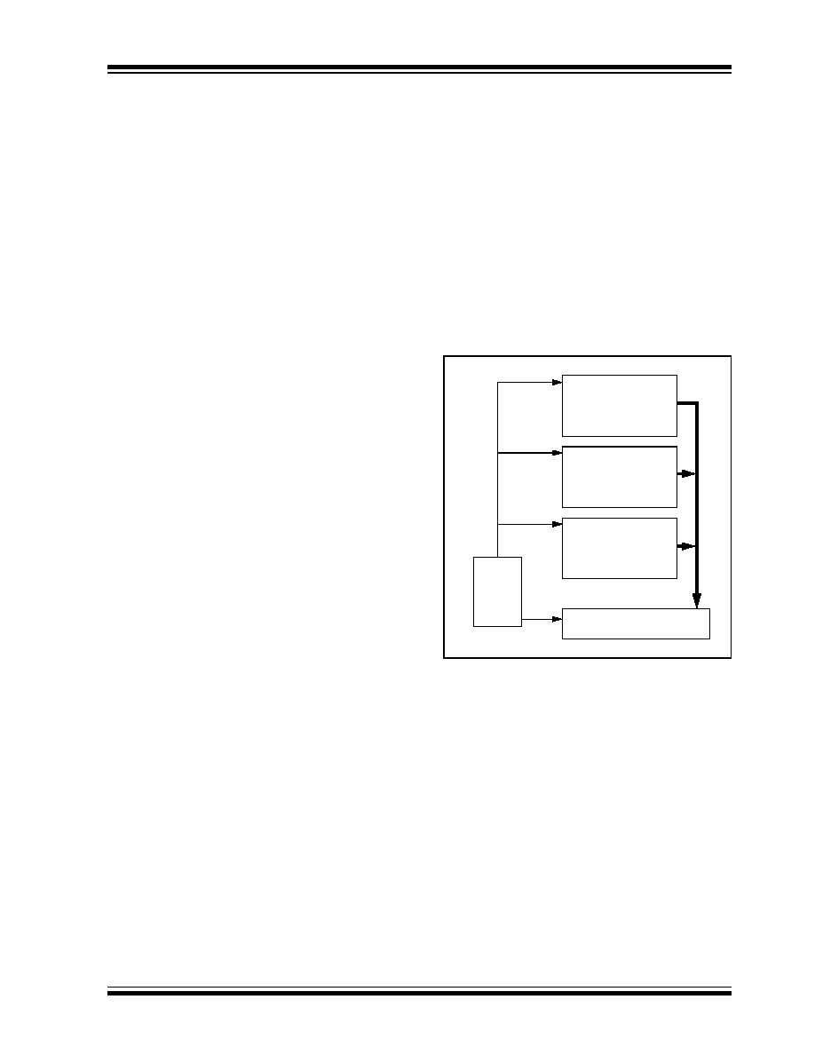
2002 Microchip Technology Inc.
Preliminary
DS41159B-page 223
PIC18FXX8
19.3.5
LOOPBACK MODE
This mode will allow internal transmission of messages
from the transmit buffers to the receive buffers, without
actually transmitting messages on the CAN bus. This
mode can be used in system development and testing.
In this mode, the ACK bit is ignored and the device will
allow incoming messages from itself, just as if they
were coming from another node. The Loopback mode
is a silent mode, meaning no messages will be trans-
mitted while in this state, including error flags or
Acknowledge signals. The TXCAN pin will revert to port
I/O while the device is in this mode. The filters and
masks can be used to allow only particular messages
to be loaded into the receive registers. The masks can
be set to all zeros to provide a mode that accepts all
messages. The Loopback mode is activated by setting
the mode request bits in the CANCON register.
19.3.6
ERROR RECOGNITION MODE
The module can be set to ignore all errors and receive
any message. The Error Recognition mode is activated
by setting the RXM<1:0> bits in the RXBnCON regis-
ters to
11
. In this mode, the data which is in the mes-
sage assembly buffer until the error time, is copied in
the receive buffer and can be read via the CPU inter-
face. In addition, the data which was on the internal
sampling of the CAN bus at the error time and the state
vector of the protocol state machine and the bit counter
CntCan, are stored in registers and can be read.
19.4
CAN Message Transmission
19.4.1
TRANSMIT BUFFERS
The PIC18FXX8 implements three Transmit Buffers
(Figure 19-2). Each of these buffers occupies 14 bytes
of SRAM and are mapped into the device memory
map.
For the MCU to have write access to the message
buffer, the TXREQ bit must be clear, indicating that the
message buffer is clear of any pending message to be
transmitted. At a minimum, the TXBnSIDH, TXBnSIDL,
and TXBnDLC registers must be loaded. If data bytes
are present in the message, the TXBnDm registers
must also be loaded. If the message is to use extended
identifiers, the TXBnEIDm registers must also be
loaded and the EXIDE bit set.
Prior to sending the message, the MCU must initialize
the TXInE bit to enable or disable the generation of an
interrupt when the message is sent. The MCU must
also initialize the TXP priority bits (see Section 19.4.2).
19.4.2
TRANSMIT PRIORITY
Transmit priority is a prioritization within the PIC18FXX8
of the pending transmittable messages. This is indepen-
dent from, and not related to, any prioritization implicit in
the message arbitration scheme built into the CAN pro-
tocol. Prior to sending the SOF, the priority of all buffers
that are queued for transmission is compared. The trans-
mit buffer with the highest priority will be sent first. If two
buffers have the same priority setting, the buffer with the
highest buffer number will be sent first. There are four
levels of transmit priority. If TXP bits for a particular mes-
sage buffer are set to
11
, that buffer has the highest pos-
sible priority. If TXP bits for a particular message buffer
are
00
, that buffer has the lowest possible priority.
FIGURE 19-2:
TRANSMIT BUFFER
BLOCK DIAGRAM
Message
Queue
Control
Transmit Byte Sequencer
TXREQ
TXB0
TXABT
TXLARB
TXERR
TXBUFF
MESSAGE
TXREQ
TXB1
TXABT
TXLARB
TXERR
TXBUFF
MESSAGE
TXREQ
TXB2
TXABT
TXLARB
TXERR
TXBUFF
MESSAGE
Message
Request

PIC18FXX8
DS41159B-page 224
Preliminary
2002 Microchip Technology Inc.
19.4.3
INITIATING TRANSMISSION
To initiate message transmission, the TXREQ bit must
be set for each buffer to be transmitted. When TXREQ
is set, the TXABT, TXLARB and TXERR bits will be
cleared.
Setting the TXREQ bit does not initiate a message
transmission, it merely flags a message buffer as ready
for transmission. Transmission will start when the
device detects that the bus is available. The device will
then begin transmission of the highest priority message
that is ready.
When the transmission has completed successfully, the
TXREQ bit will be cleared, the TXBnIF bit will be set, and
an interrupt will be generated if the TXBnIE bit is set.
If the message transmission fails, the TXREQ will remain
set, indicating that the message is still pending for trans-
mission and one of the following condition flags will be
set. If the message started to transmit but encountered
an error condition, the TXERR and the IRXIF bits will be
set and an interrupt will be generated. If the message lost
arbitration, the TXLARB bit will be set.
19.4.4
ABORTING TRANSMISSION
The MCU can request to abort a message by clearing
the TXREQ bit associated with the corresponding mes-
sage buffer (TXBnCON<3>). Setting the ABAT bit
(CANCON<4>) will request an abort of all pending mes-
sages. If the message has not yet started transmission,
or if the message started but is interrupted by loss of
arbitration or an error, the abort will be processed. The
abort is indicated when the module sets the ABT bits for
the corresponding buffer (TXBnCON<6>). If the mes-
sage has started to transmit, it will attempt to transmit the
current message fully. If the current message is transmit-
ted fully and is not lost to arbitration or an error, the ABT
bit will not be set, because the message was transmitted
successfully. Likewise, if a message is being transmitted
during an abort request and the message is lost to arbi-
tration or an error, the message will not be retransmitted
and the ABT bit will be set, indicating that the message
was successfully aborted.
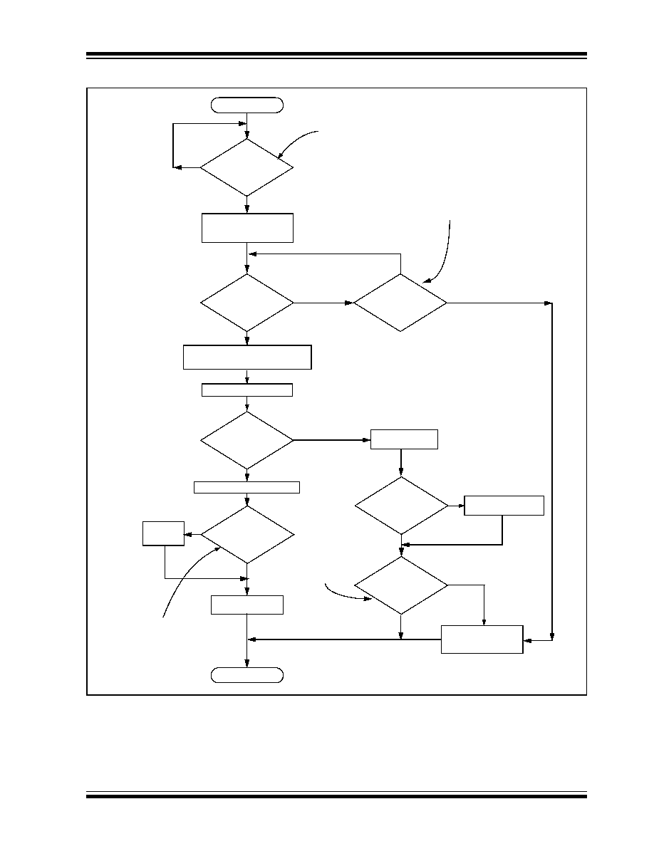
2002 Microchip Technology Inc.
Preliminary
DS41159B-page 225
PIC18FXX8
FIGURE 19-3:
TRANSMIT MESSAGE FLOW CHART
Start
Is
CAN bus Available
to Start Transmission
No
Examine TXPRI <1:0> to
Are any
TXREQ
?
bits = 1
The message transmission sequence begins when
the device determines that the TXREQ for any of the
transmit registers has been set.
Clear: TXABT, TXLARB
and TXERR
Yes
?
Is
TXREQ = 0
ABAT = 1
Clearing the TXREQ bit while it is set, or setting
the ABAT bit before the message has started
transmission, will abort the message.
No
Begin Transmission (SOF)
Abort Transmission:
Was
Message Transmitted
Successfully?
No
Yes
Set TXREQ = 0
Is
TXIE = 1?
Generate
Interrupt
Yes
Yes
Set TXABT = 1
Set
Set
TXERR = 1
Yes
No
Determine Highest Priority Message
No
?
Is
TXLARB = 1?
The TXIE bit determines if an inter-
rupt should be generated when a
message is successfully transmitted.
END
Is
TXREQ = 0
or TXABT = 1
?
Yes
No
TXBUFE = 1
Yes
A message can also be
aborted, if a message
error or lost arbitration
condition occurred during
transmission.
Arbitration Lost During
Transmission
No
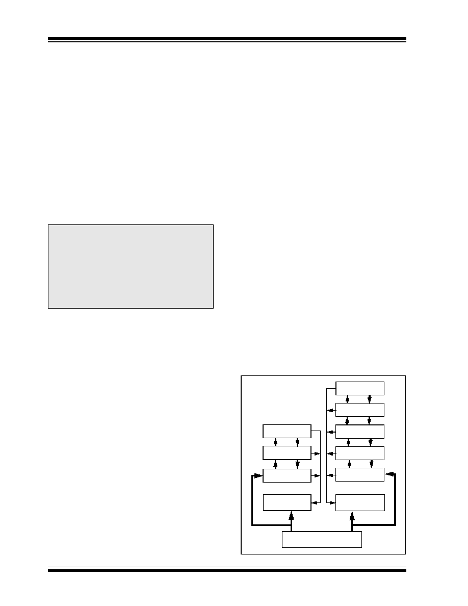
PIC18FXX8
DS41159B-page 226
Preliminary
2002 Microchip Technology Inc.
19.5
Message Reception
19.5.1
RECEIVE MESSAGE BUFFERING
The PIC18FXX8 includes two full receive buffers with
multiple acceptance filters for each. There is also a
separate Message Assembly Buffer (MAB), which acts
as a third receive buffer (see Figure 19-4).
19.5.2
RECEIVE BUFFERS
Of the three receive buffers, the MAB is always commit-
ted to receiving the next message from the bus. The
remaining two receive buffers are called RXB0 and
RXB1 and can receive a complete message from the
protocol engine. The MCU can access one buffer while
the other buffer is available for message reception, or
holding a previously received message.
The MAB assembles all messages received. These
messages will be transferred to the RXBn buffers, only
if the acceptance filter criteria are met.
When a message is moved into either of the receive
buffers, the appropriate RXBnIF bit is set. This bit must
be cleared by the MCU when it has completed process-
ing the message in the buffer, in order to allow a new
message to be received into the buffer. This bit pro-
vides a positive lockout to ensure that the MCU has fin-
ished with the message before the PIC18FXX8
attempts to load a new message into the receive buffer.
If the RXBnIE bit is set, an interrupt will be generated to
indicate that a valid message has been received.
19.5.3
RECEIVE PRIORITY
RXB0 is the higher priority buffer and has two message
acceptance filters associated with it. RXB1 is the lower
priority buffer and has four acceptance filters associ-
ated with it. The lower number of acceptance filters
makes the match on RXB0 more restrictive and implies
a higher priority for that buffer. Additionally, the
RXB0CON register can be configured such that if
RXB0 contains a valid message and another valid mes-
sage is received, an overflow error will not occur and
the new message will be moved into RXB1, regardless
of the acceptance criteria of RXB1. There are also two
programmable acceptance filter masks available, one
for each receive buffer (see Section 4.5).
When a message is received, bits <3:0> of the
RXBnCON register will indicate the acceptance filter
number that enabled reception and whether the
received message is a remote transfer request.
The RXM bits set special Receive modes. Normally,
these bits are set to `
00
' to enable reception of all valid
messages, as determined by the appropriate accep-
tance filters. In this case, the determination of whether
or not to receive standard or extended messages is
determined by the EXIDE bit in the acceptance filter
register. If the RXM bits are set to `
01
' or `
10
', the
receiver will accept only messages with standard or
extended identifiers, respectively. If an acceptance fil-
ter has the EXIDE bit set, such that it does not corre-
spond with the RXM mode, that acceptance filter is
rendered useless. These two modes of RXM bits can
be used in systems where it is known that only standard
or extended messages will be on the bus. If the RXM
bits are set to `
11
', the buffer will receive all messages,
regardless of the values of the acceptance filters. Also,
if a message has an error before the end of frame, that
portion of the message assembled in the MAB before
the error frame, will be loaded into the buffer. This
mode has some value in debugging a CAN system and
would not be used in an actual system environment.
19.5.4
TIME-STAMPING
The CAN module can be programmed to generate a
time-stamp for every message that is received. When
enabled, the module generates a capture signal for
CCP1, which in turns captures the value of either
Timer1 or Timer3. This value can be used as the
message time-stamp.
To use the time-stamp capability, the CANCAP bit
(CIOCAN<4>) must be set. This replaces the capture
input for CCP1 with the signal generated from the CAN
module. In addition, CCP1CON<3:0> must be set to
`
0011
' to enable the CCP special event trigger for CAN
events.
FIGURE 19-4:
RECEIVE BUFFER BLOCK
DIAGRAM
Note:
The entire contents of the MAB are moved
into the receive buffer once a message is
accepted. This means that, regardless of
the type of identifier (standard or extended)
and the number of data bytes received, the
entire receive buffer is overwritten with the
MAB contents. Therefore, the contents of
all registers in the buffer must be assumed
to have been modified when any message
is received.
Acceptance Mask
RXM0
Acceptance Filter
RXF0
Acceptance Filter
RXF1
Message Assembly Buffer
Acceptance Filter
RXM2
Acceptance Filter
RXF3
Acceptance Filter
RXF4
Acceptance Filter
RXF5
Acceptance Mask
RXM1
RXB0
RXB1
Accept
Accept
Data and
Identifier
Data and
Identifier
Identifier
Identifier
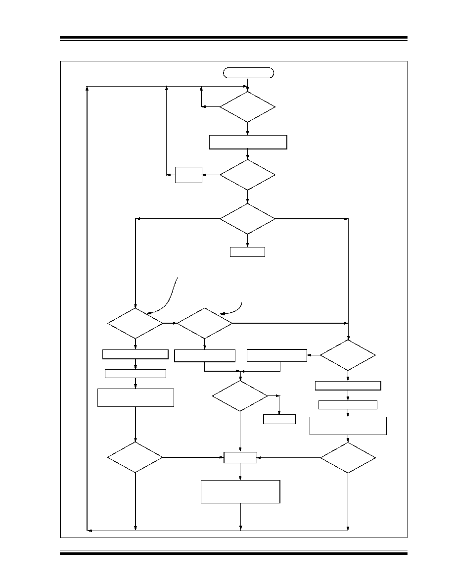
2002 Microchip Technology Inc.
Preliminary
DS41159B-page 227
PIC18FXX8
FIGURE 19-5:
MESSAGE RECEPTION FLOW CHART
Start
Detect
Start of
Message?
Valid
Message
Received?
Generate
Error
Message
Identifier meets
a Filter Criteria?
Is
RXFUL = 0?
Go to Start
Move Message into RXB0
Set RXRDY = 1
Set FILHIT <2:0>
Is
RXFUL = 0?
Move Message into RXB1
Set RXRDY = 1
Yes, meets criteria
for RXBO
Yes, meets criteria
for RXB1
No
Generate
Interrupt
Yes
Yes
No
No
Yes
Yes
No
No
Yes
Yes
Frame
The RXFUL bit determines if the
receive register is empty and able
to accept a new message.
No
Yes
No
Generate Overrun Error:
Begin Loading Message into
Message Assembly Buffer (MAB)
according to which Filter
Criteria was met
Is
RXIE = 1?
Is
RXIE = 1?
Is
RX0DBEN = 1?
The RXB0DBEN bit determines if
RXB0 can rollover into RXB1 if it is
full.
Set RXB0OVFL
Generate Overrun Error:
Set RXB1OVFL
Is
ERRIE = 1?
No
Go to Start
Yes
No
Set FILHIT <0>
according to which Filter
Criteria was met
Set CANSTAT <3:0> according
to which Receive Buffer the
Message was loaded into
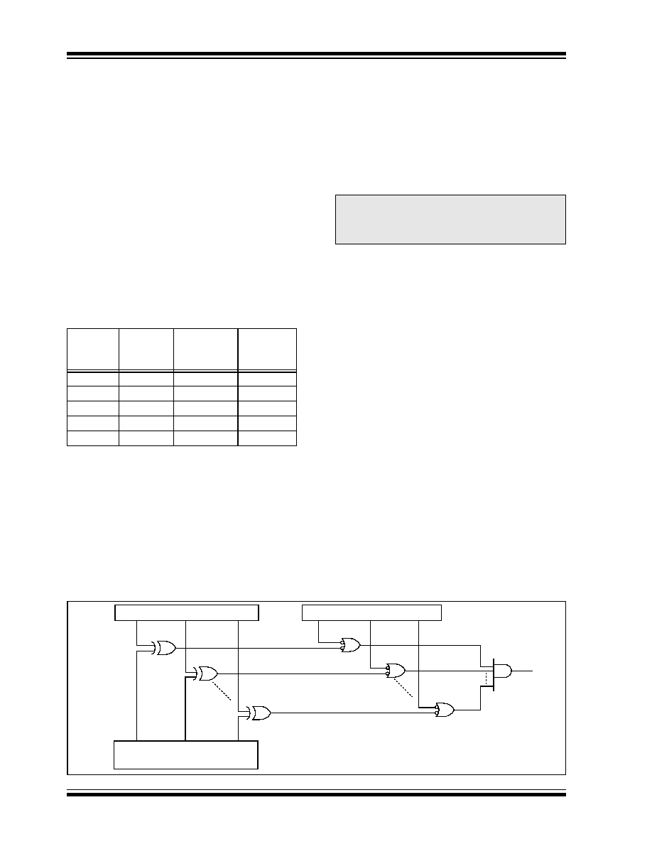
PIC18FXX8
DS41159B-page 228
Preliminary
2002 Microchip Technology Inc.
19.6
Message Acceptance Filters and
Masks
The Message Acceptance Filters and Masks are used
to determine if a message in the message assembly
buffer should be loaded into either of the receive buff-
ers. Once a valid message has been received into the
MAB, the identifier fields of the message are compared
to the filter values. If there is a match, that message will
be loaded into the appropriate receive buffer. The filter
masks are used to determine which bits in the identifier
are examined with the filters. A truth table is shown
below in Table 19-2 that indicates how each bit in the
identifier is compared to the masks and filters to deter-
mine if a message should be loaded into a receive
buffer. The mask, essentially determines which bits to
apply the acceptance filters to. If any mask bit is set to
a zero, then that bit will automatically be accepted,
regardless of the filter bit.
TABLE 19-2:
FILTER/MASK TRUTH TABLE
As shown in the Receive Buffers Block Diagram
(Figure 19-4), acceptance filters RXF0 and RXF1, and
filter mask RXM0 are associated with RXB0. Filters
RXF2, RXF3, RXF4, and RXF5 and mask RXM1 are
associated with RXB1. When a filter matches and a
message is loaded into the receive buffer, the filter num-
ber that enabled the message reception is loaded into
the FILHIT bit(s).
For RXB1, the RXB1CON register contains the
FILHIT<2:0> bits. They are coded as follows:
�
101
= Acceptance Filter 5 (RXF5)
�
100
= Acceptance Filter 4 (RXF4)
�
011
= Acceptance Filter 3 (RXF3)
�
010
= Acceptance Filter 2 (RXF2)
�
001
= Acceptance Filter 1 (RXF1)
�
000
= Acceptance Filter 0 (RXF0)
The coding of the RXB0DBEN bit enables these three
bits to be used similarly to the FILHIT bits and to distin-
guish a hit on filter RXF0 and RXF1, in either RXB0, or
after a rollover into RXB1.
�
111
= Acceptance Filter 1 (RXF1)
�
110
= Acceptance Filter 0 (RXF0)
�
001
= Acceptance Filter 1 (RXF1)
�
000
= Acceptance Filter 0
If the RXB0DBEN bit is clear, there are six codes cor-
responding to the six filters. If the RXB0DBEN bit is set,
there are six codes corresponding to the six filters, plus
two additional codes corresponding to RXF0 and RXF1
filters that rollover into RXB1.
If more than one acceptance filter matches, the FILHIT
bits will encode the binary value of the lowest num-
bered filter that matched. In other words, if filter RXF2
and filter RXF4 match, FILHIT will be loaded with the
value for RXF2. This essentially prioritizes the accep-
tance filters with a lower number filter having higher pri-
ority. Messages are compared to filters in ascending
order of filter number.
The mask and filter registers can only be modified
when the PIC18FXX8 is in Configuration mode. The
mask and filter registers cannot be read outside of Con-
figuration mode. When outside of Configuration mode,
all mask and filter registers will be read as `0'.
FIGURE 19-6:
MESSAGE ACCEPTANCE MASK AND FILTER OPERATION
Mask
bit n
Filter bit n
Message
Identifier
bit n001
Accept or
Reject
bit n
0
X
X
Accept
1
0
0
Accept
1
0
1
Reject
1
1
0
Reject
1
1
1
Accept
Legend:
X
= don't care
Note:
000
and
001
can only occur if the
RXB0DBEN bit is set in the RXB0CON
register, allowing RXB0 messages to
rollover into RXB1.
Acceptance Filter Register
Acceptance Mask Register
RxRqst
Message Assembly Buffer
RXFn
0
RXFn
1
RXFn
n
RXMn
0
RXMn
1
RXMn
n
Identifier
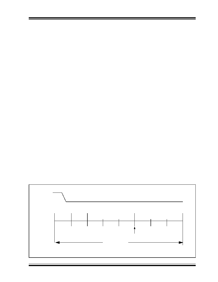
2002 Microchip Technology Inc.
Preliminary
DS41159B-page 229
PIC18FXX8
19.7
Baud Rate Setting
All nodes on a given CAN bus must have the same
nominal bit rate. The CAN protocol uses Non-Return-
to-Zero (NRZ) coding, which does not encode a clock
within the data stream. Therefore, the receive clock
must be recovered by the receiving nodes and
synchronized to the transmitters clock.
As oscillators and transmission time may vary from
node to node; the receiver must have some type of
Phase Lock Loop (PLL) synchronized to data transmis-
sion edges to synchronize and maintain the receiver
clock. Since the data is NRZ coded, it is necessary to
include bit stuffing to ensure that an edge occurs at
least every six bit times, to maintain the Digital Phase
Lock Loop (DPLL) synchronization.
The bit timing of the PIC18FXX8 is implemented using
a DPLL that is configured to synchronize to the incom-
ing data, and provides the nominal timing for the trans-
mitted data. The DPLL breaks each bit time into
multiple segments, made up of minimal periods of time
called the Time Quanta (T
Q
).
Bus timing functions executed within the bit time frame,
such as synchronization to the local oscillator, network
transmission delay compensation, and sample point
positioning, are defined by the programmable bit timing
logic of the DPLL.
All devices on the CAN bus must use the same bit rate.
However, all devices are not required to have the same
master oscillator clock frequency. For the different clock
frequencies of the individual devices, the bit rate has to
be adjusted by appropriately setting the baud rate
prescaler and number of time quanta in each segment.
The Nominal Bit Rate is the number of bits transmitted
per second, assuming an ideal transmitter with an ideal
oscillator, in the absence of resynchronization. The
nominal bit rate is defined to be a maximum of 1 Mb/s.
The Nominal Bit Time is defined as
T
BIT
= 1 / Nominal Bit rate
The Nominal Bit Time can be thought of as being
divided into separate, non-overlapping time segments.
These segments (Figure 19-7) include:
� Synchronization Segment (Sync_Seg)
� Propagation Time Segment (Prop_Seg)
� Phase Buffer Segment 1 (Phase_Seg1)
� Phase Buffer Segment 2 (Phase_Seg2)
The time segments (and thus the Nominal Bit Time) are
in turn made up of integer units of time called Time
Quanta or T
Q
(see Figure 19-7). By definition, the nom-
inal bit time is programmable from a minimum of 8 T
Q
to a maximum of 25 T
Q
. Also, by definition, the mini-
mum Nominal Bit Time is 1
�
s, corresponding to a max-
imum 1 Mb/s rate. The actual duration is given by the
relationship
Nominal Bit Time = T
Q
* (Sync_Seg + Prop_Seg +
Phase_Seg1 + Phase_Seg2)
The Time Quantum is a fixed unit derived from the
oscillator period. It is also defined by the programmable
baud rate prescaler with integer values from 1 to 64, in
addition to a fixed divide-by-two for clock generation.
Mathematically, this is
T
Q
(
�
s) = (2 * (BRP+1)) / F
OSC
(MHz)
or
T
Q
(
�
s) = (2 * (BRP+1)) * T
OSC
(�s)
where F
OSC
is the clock frequency, T
OSC
is the corre-
sponding oscillator period, and BRP is an integer (0
through 63) represented by the binary values of
BRGCON1<5:0>.
FIGURE 19-7:
BIT TIME PARTITIONING
Input
Sync
Propagation
Segment
Phase
Segment 1
Phase
Segment 2
Sample Point
T
Q
Nominal Bit Time
Bit
Time
Intervals
Signal
Segment

PIC18FXX8
DS41159B-page 230
Preliminary
2002 Microchip Technology Inc.
19.7.1
TIME QUANTA
As already mentioned, the Time Quanta is a fixed unit
derived from the oscillator period and baud rate pres-
caler. Its relationship to T
BIT
and the Nominal Bit Rate
is shown in Example 19-2.
EXAMPLE 19-2:
CALCULATING T
Q
,
NOMINAL BIT RATE AND
NOMINAL BIT TIME
The frequencies of the oscillators in the different nodes
must be coordinated in order to provide a system wide
specified nominal bit time. This means that all oscilla-
tors must have a T
OSC
that is an integral divisor of T
Q
.
It should also be noted that although the number of T
Q
is programmable from 4 to 25, the usable minimum is
8 T
Q
.
A bit time of less than 8 T
Q
in length is not
guaranteed to operate correctly.
19.7.2
SYNCHRONIZATION SEGMENT
This part of the bit time is used to synchronize the var-
ious CAN nodes on the bus. The edge of the input sig-
nal is expected to occur during the sync segment. The
duration is 1 T
Q
.
19.7.3
PROPAGATION SEGMENT
This part of the bit time is used to compensate for phys-
ical delay times within the network. These delay times
consist of the signal propagation time on the bus line
and the internal delay time of the nodes. The length of
the Propagation Segment can be programmed from
1 T
Q
to 8 T
Q
by setting the PRSEG2:PRSEG0 bits.
19.7.4
PHASE BUFFER SEGMENTS
The Phase Buffer Segments are used to optimally
locate the sampling point of the received bit, within the
nominal bit time. The sampling point occurs between
phase segment 1 and phase segment 2. These seg-
ments can be lengthened or shortened by the resyn-
chronization process. The end of phase segment 1
determines the sampling point within a bit time. Phase
segment 1 is programmable from 1 T
Q
to 8 T
Q
in dura-
tion. Phase segment 2 provides delay before the next
transmitted data transition and is also programmable
from 1 T
Q
to 8 T
Q
in duration. However, due to IPT
requirements, the actual minimum length of phase seg-
ment 2 is 2 T
Q
, or it may be defined to be equal to the
greater of phase segment 1 or the Information
Processing Time (IPT).
19.7.5
SAMPLE POINT
The Sample Point is the point of time at which the bus
level is read and the value of the received bit is deter-
mined. The sampling point occurs at the end of phase
segment 1. If the bit timing is slow and contains many
T
Q
, it is possible to specify multiple sampling of the bus
line at the sample point. The value of the received bit is
determined to be the value of the majority decision of
three values. The three samples are taken at the sam-
ple point, and twice before, with a time of T
Q
/2 between
each sample.
19.7.6
INFORMATION PROCESSING TIME
The Information Processing Time (IPT) is the time seg-
ment, starting at the sample point that is reserved for
calculation of the subsequent bit level. The CAN spec-
ification defines this time to be less than or equal to
2 T
Q
. The PIC18FXX8 defines this time to be 2 T
Q
.
Thus, phase segment 2 must be at least 2 T
Q
long.
T
Q
(
�
s) = (2 * (BRP+1)) / F
OSC
(MHz)
T
BIT
(
�
s) = T
Q
(
�
s) * number of T
Q
per bit interval
Nominal Bit Rate (bits/s) = 1 / T
BIT
CASE 1:
For F
OSC
= 16 MHz, BRP<5:0> = 00h, and
Nominal Bit Time = 8 T
Q
:
T
Q
= (2*1) / 16 = 0.125
�
s (125 ns)
T
BIT
= 8 * 0.125 = 1
�
s (10
-6
s)
Nominal Bit Rate = 1 / 10
-6
= 10
6
bits/s (1 Mb/s)
CASE 2:
For F
OSC
= 20 MHz, BRP<5:0> = 01h, and
Nominal Bit Time = 8 T
Q
:
T
Q
= (2*2) / 20 = 0.2
�
s (200 ns)
T
BIT
= 8 * 0.2 = 1.6
�
s (1.6 * 10
-6
S
)
Nominal Bit Rate = 1 / 1.6 * 10
-6
s = 625,000 bits/s
(625 Kb/s)
CASE 3:
For F
OSC
= 25 MHz, BRP<5:0> = 3Fh, and
Nominal Bit Time = 25 T
Q
:
T
Q
= (2*64) / 25 = 5.12
�
s
T
BIT
= 25 * 5.12 = 128
�
s (1.28 * 10
-4
s)
Nominal Bit Rate = 1 / 1.28 * 10
-4
= 7813 bits/s
(7.8 Kb/s)
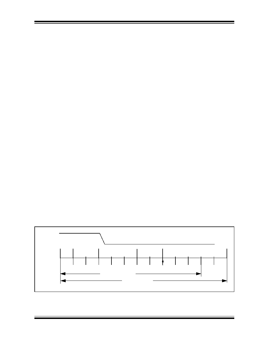
2002 Microchip Technology Inc.
Preliminary
DS41159B-page 231
PIC18FXX8
19.8
Synchronization
To compensate for phase shifts between the oscillator
frequencies of each of the nodes on the bus, each CAN
controller must be able to synchronize to the relevant
signal edge of the incoming signal. When an edge in
the transmitted data is detected, the logic will compare
the location of the edge to the expected time (Sync
Seg). The circuit will then adjust the values of phase
segment 1 and phase segment 2, as necessary. There
are two mechanisms used for synchronization.
19.8.1
HARD SYNCHRONIZATION
Hard synchronization is only done when there is a
recessive to dominant edge during a BUS IDLE condi-
tion, indicating the start of a message. After hard syn-
chronization, the bit time counters are restarted with
Sync Seg. Hard synchronization forces the edge which
has occurred to lie within the synchronization segment
of the restarted bit time. Due to the rules of synchroni-
zation, if a hard synchronization occurs, there will not
be a resynchronization within that bit time.
19.8.2
RESYNCHRONIZATION
As a result of resynchronization, phase segment 1 may
be lengthened, or phase segment 2 may be shortened.
The amount of lengthening or shortening of the phase
buffer segments has an upper bound given by the Syn-
chronization Jump Width (SJW). The value of the SJW
will be added to phase segment 1 (see Figure 19-8), or
subtracted from phase segment 2 (see Figure 19-9).
The SJW is programmable between 1 T
Q
and 4 T
Q
.
Clocking information will only be derived from reces-
sive to dominant transitions. The property, that only a
fixed maximum number of successive bits have the
same value, ensures resynchronization to the bit
stream during a frame.
The phase error of an edge is given by the position of
the edge relative to Sync Seg, measured in T
Q
. The
phase error is defined in magnitude of T
Q
as follows:
� e = 0 if the edge lies within SYNCESEG.
� e > 0 if the edge lies before the SAMPLE POINT.
� e < 0 if the edge lies after the SAMPLE POINT of
the previous bit
If the magnitude of the phase error is less than, or equal
to, the programmed value of the synchronization jump
width, the effect of a resynchronization is the same as
that of a hard synchronization.
If the magnitude of the phase error is larger than the
synchronization jump width, and if the phase error is
positive, then phase segment 1 is lengthened by an
amount equal to the synchronization jump width.
If the magnitude of the phase error is larger than the
resynchronization jump width, and if the phase error is
negative, then phase segment 2 is shortened by an
amount equal to the synchronization jump width.
19.8.3
SYNCHRONIZATION RULES
� Only one synchronization within one bit time is
allowed.
� An edge will be used for synchronization only if
the value detected at the previous sample point
(previously read bus value) differs from the bus
value immediately after the edge.
� All other recessive to dominant edges fulfilling
rules 1 and 2, will be used for resynchronization,
with the exception that a node transmitting a dom-
inant bit will not perform a resynchronization as a
result of a recessive to dominant edge with a
positive phase error.
FIGURE 19-8:
LENGTHENING A BIT PERIOD (ADDING SJW TO PHASE SEGMENT 1)
Input
Sync
Prop
Segment
Phase
Segment 1
Phase
Segment 2
SJW
Sample Point
T
Q
Signal
Nominal Bit Length
Actual Bit Length
Bit
Time
Segments
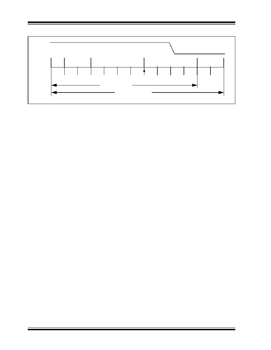
PIC18FXX8
DS41159B-page 232
Preliminary
2002 Microchip Technology Inc.
FIGURE 19-9:
SHORTENING A BIT PERIOD (SUBTRACTING SJW FROM PHASE SEGMENT 2)
19.9
Programming Time Segments
Some requirements for programming of the time
segments:
� Prop Seg + Phase Seg 1
Phase Seg 2
� Phase Seg 2
Sync Jump Width.
For example, assume that a 125 kHz CAN baud rate is
desired, using 20 MHz for F
OSC
. With a T
OSC
of 50 ns,
a baud rate prescaler value of 04h gives a T
Q
of 500 ns.
To obtain a Nominal Bit Rate of 125 kHz, the Nominal
Bit Time must be 8
�
s, or 16 T
Q
.
Using 1 T
Q
for the Sync Segment, 2 T
Q
for the Propa-
gation Segment and 7 T
Q
for Phase Segment 1 would
place the sample point at 10 T
Q
after the transition.
This leaves 6 T
Q
for Phase Segment 2.
By the rules above, the Sync Jump Width could be the
maximum of 4 T
Q
. However, normally a large SJW is
only necessary when the clock generation of the differ-
ent nodes is inaccurate or unstable, such as using
ceramic resonators. Typically, an SJW of 1 is enough.
19.10 Oscillator Tolerance
As a rule of thumb, the bit timing requirements allow
ceramic resonators to be used in applications with
transmission rates of up to 125 Kbit/sec. For the full bus
speed range of the CAN protocol, a quartz oscillator is
required. A maximum node-to-node oscillator variation
of 1.7% is allowed.
19.11 Bit Timing Configuration
Registers
The configuration registers (BRGCON1, BRGCON2,
BRGCON3) control the bit timing for the CAN bus inter-
face. These registers can only be modified when the
PIC18FXX8 is in Configuration mode.
19.11.1
BRGCON1
The BRP bits control the baud rate prescaler. The
SJW<1:0> bits select the synchronization jump width in
terms of multiples of T
Q
.
19.11.2
BRGCON2
The PRSEG bits set the length of the propagation seg-
ment in terms of T
Q
. The SEG1PH bits set the length of
phase segment 1 in T
Q
. The SAM bit controls how
many times the RXCAN pin is sampled. Setting this bit
to a `1' causes the bus to be sampled three times; twice
at T
Q
/2 before the sample point, and once at the normal
sample point (which is at the end of phase segment 1).
The value of the bus is determined to be the value read
during at least two of the samples. If the SAM bit is set
to a `0', then the RXCAN pin is sampled only once at
the sample point. The SEG2PHTS bit controls how the
length of phase segment 2 is determined. If this bit is
set to a `1', then the length of phase segment 2 is deter-
mined by the SEG2PH bits of BRGCON3. If the
SEG2PHTS bit is set to a `0', then the length of phase
segment 2 is the greater of phase segment 1 and the
information processing time (which is fixed at 2 T
Q
for
the PIC18FXX8).
19.11.3
BRGCON3
The PHSEG2<2:0> bits set the length (in T
Q
) of phase
segment 2, if the SEG2PHTS bit is set to a `1'. If the
SEG2PHTS bit is set to a `0', then the PHSEG2<2:0>
bits have no effect.
Sync
Prop
Segment
Phase
Segment 1
Phase
Segment 2
SJW
T
Q
Sample Point
Nominal Bit Length
Actual Bit Length

2002 Microchip Technology Inc.
Preliminary
DS41159B-page 233
PIC18FXX8
19.12 Error Detection
The CAN protocol provides sophisticated error detection
mechanisms. The following errors can be detected.
19.12.1
CRC ERROR
With the Cyclic Redundancy Check (CRC), the trans-
mitter calculates special check bits for the bit
sequence, from the start of a frame until the end of the
data field. This CRC sequence is transmitted in the
CRC field. The receiving node also calculates the CRC
sequence using the same formula and performs a com-
parison to the received sequence. If a mismatch is
detected, a CRC error has occurred and an error frame
is generated. The message is repeated.
19.12.2
ACKNOWLEDGE ERROR
In the Acknowledge field of a message, the transmitter
checks if the Acknowledge slot (which was sent out as
a recessive bit) contains a dominant bit. If not, no other
node has received the frame correctly. An Acknowl-
edge Error has occurred; an error frame is generated
and the message will have to be repeated.
19.12.3
FORM ERROR
lf a node detects a dominant bit in one of the four seg-
ments, including end of frame, interframe space,
Acknowledge delimiter, or CRC delimiter, then a Form
Error has occurred and an error frame is generated.
The message is repeated.
19.12.4
BIT ERROR
A Bit Error occurs if a transmitter sends a dominant bit
and detects a recessive bit, or if it sends a recessive bit
and detects a dominant bit, when monitoring the actual
bus level and comparing it to the just transmitted bit. In
the case where the transmitter sends a recessive bit
and a dominant bit is detected during the arbitration
field and the Acknowledge slot, no bit error is
generated because normal arbitration is occurring.
19.12.5
STUFF BIT ERROR
lf, between the start of frame and the CRC delimiter, six
consecutive bits with the same polarity are detected,
the bit stuffing rule has been violated. A Stuff Bit Error
occurs and an error frame is generated. The message
is repeated.
19.12.6
ERROR STATES
Detected errors are made public to all other nodes via
error frames. The transmission of the erroneous mes-
sage is aborted and the frame is repeated as soon as
possible. Furthermore, each CAN node is in one of the
three error states "error-active", "error-passive" or "bus-
off" according to the value of the internal error counters.
The error-active state is the usual state, where the bus
node can transmit messages and activate error frames
(made of dominant bits), without any restrictions. In the
error-passive state, messages and passive error
frames (made of recessive bits) may be transmitted.
The bus-off state makes it temporarily impossible for
the station to participate in the bus communication.
During this state, messages can neither be received
nor transmitted.
19.12.7
ERROR MODES AND ERROR
COUNTERS
The PIC18FXX8 contains two error counters: the
Receive Error Counter (RXERRCNT), and the Trans-
mit Error Counter (TXERRCNT). The values of both
counters can be read by the MCU. These counters are
incremented or decremented in accordance with the
CAN bus specification.
The PIC18FXX8 is error-active if both error counters
are below the error-passive limit of 128. It is error-
passive if at least one of the error counters equals or
exceeds 128. It goes to bus-off if the transmit error
counter equals or exceeds the bus-off limit of 256. The
device remains in this state until the bus-off recovery
sequence is received. The bus-off recovery sequence
consists of 128 occurrences of 11 consecutive reces-
sive bits (see Figure 19-10). Note that the CAN mod-
ule, after going bus-off, will recover back to error-active
without any intervention by the MCU, if the bus remains
IDLE for 128 X 11 bit times. If this is not desired, the
error Interrupt Service Routine should address this.
The current Error mode of the CAN module can be read
by the MCU via the COMSTAT register.
Additionally, there is an error state warning flag bit,
EWARN, which is set if at least one of the error
counters equals or exceeds the error warning limit of
96. EWARN is reset if both error counters are less than
the error warning limit.
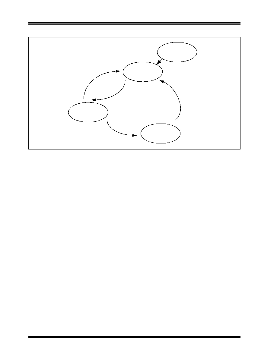
PIC18FXX8
DS41159B-page 234
Preliminary
2002 Microchip Technology Inc.
FIGURE 19-10:
ERROR MODES STATE DIAGRAM
19.13 CAN Interrupts
The module has several sources of interrupts. Each of
these interrupts can be individually enabled or dis-
abled. The CANINTF register contains interrupt flags.
The CANINTE register contains the enables for the 8
main interrupts. A special set of read only bits in the
CANSTAT register, the ICODE bits, can be used in
combination with a jump table for efficient handling of
interrupts.
All interrupts have one source, with the exception of the
Error Interrupt. Any of the Error Interrupt sources can set
the Error Interrupt Flag. The source of the Error Interrupt
can be determined by reading the Communication
Status register, COMSTAT.
The interrupts can be broken up into two categories:
receive and transmit interrupts.
The receive related interrupts are:
� Receive Interrupts
� Wake-up Interrupt
� Receiver Overrun Interrupt
� Receiver Warning Interrupt
� Receiver Error-Passive Interrupt
The transmit related interrupts are:
� Transmit Interrupts
� Transmitter Warning Interrupt
� Transmitter Error-Passive Interrupt
� Bus-Off Interrupt
19.13.1
INTERRUPT CODE BITS
The source of a pending interrupt is indicated in the
ICODE (interrupt code) bits of the CANSTAT register
(ICOD<2:0>). Interrupts are internally prioritized such
that the higher priority interrupts are assigned lower
ICODE values. Once the highest priority interrupt con-
dition has been cleared, the code for the next highest
priority interrupt that is pending (if any), will be reflected
by the ICODE bits (see Table 19-3, following page).
Note that only those interrupt sources that have their
associated CANINTE enable bit set will be reflected in
the ICODE bits.
19.13.2
TRANSMIT INTERRUPT
When the Transmit Interrupt is enabled, an interrupt will
be generated when the associated transmit buffer
becomes empty and is ready to be loaded with a new
message. The TXBnIF bit will be set to indicate the
source of the interrupt. The interrupt is cleared by the
MCU resetting the TXBnIF bit to a `
0
'.
19.13.3
RECEIVE INTERRUPT
When the Receive Interrupt is enabled, an interrupt will
be generated when a message has been successfully
received and loaded into the associated receive buffer.
This interrupt is activated immediately after receiving
the EOF field. The RXBnIF bit will be set to indicate the
source of the interrupt. The interrupt is cleared by the
MCU resetting the RXBnIF bit to a `
0
'.
Bus-
Off
Error-
Active
Error-
Passive
RXERRCNT < 127 or
TXERRCNT < 127
RXERRCNT > 127 or
TXERRCNT > 127
TXERRCNT > 255
128 occurrences of
11 consecutive
"recessive" bits
RESET
2002 Microchip Technology Inc.
Preliminary
DS41159B-page 235
PIC18FXX8
TABLE 19-3:
VALUES FOR ICODE<2:0>
19.13.4
MESSAGE ERROR INTERRUPT
When an error occurs during transmission or reception
of a message, the message error flag IRXIF will be set
and if the IRXIE bit is set, an interrupt will be generated.
This is intended to be used to facilitate baud rate deter-
mination when used in conjunction with Listen Only
mode.
19.13.5
BUS ACTIVITY WAKE-UP
INTERRUPT
When the PIC18FXX8 is in SLEEP mode and the Bus
Activity Wake-up Interrupt is enabled, an interrupt will
be generated, and the WAKIF bit will be set when activ-
ity is detected on the CAN bus. This interrupt causes
the PIC18FXX8 to exit SLEEP mode. The interrupt is
reset by the MCU, clearing the WAKIF bit.
19.13.6
ERROR INTERRUPT
When the Error Interrupt is enabled, an interrupt is gen-
erated if an overflow condition occurs, or if the error
state of transmitter or receiver has changed. The error
flags in COMSTAT will indicate one of the following
conditions.
19.13.6.1
Receiver Overflow
An overflow condition occurs when the MAB has
assembled a valid received message (the message
meets the criteria of the acceptance filters) and the
receive buffer associated with the filter is not available
for loading of a new message. The associated
COMSTAT.RXnOVFL bit will be set to indicate the
overflow condition. This bit must be cleared by the
MCU.
19.13.6.2
Receiver Warning
The receive error counter has reached the MCU
warning limit of 96.
19.13.6.3
Transmitter Warning
The transmit error counter has reached the MCU
warning limit of 96.
19.13.6.4
Receiver Bus Passive
The receive error counter has exceeded the error-
passive limit of 127 and the device has gone to
error-passive state.
19.13.6.5
Transmitter Bus Passive
The transmit error counter has exceeded the error-
passive limit of 127 and the device has gone to
error- passive state.
19.13.6.6
Bus-Off
The transmit error counter has exceeded 255 and the
device has gone to bus-off state.
19.13.7
INTERRUPT ACKNOWLEDGE
Interrupts are directly associated with one or more sta-
tus flags in the PIR register. Interrupts are pending as
long as one of the flags is set. Once an interrupt flag is
set by the device, the flag can not be reset by the
microcontroller until the interrupt condition is removed.
ICOD
<2:0>
Interrupt
Boolean Expression
000
None
ERR�WAK�TX0�TX1�TX2�RX0�
RX1
001
Error
ERR
010
TXB2
ERR�TX0�TX1�TX2
011
TXB1
ERR�TX0�TX1
100
TXB0
ERR�TX0
101
RXB1
ERR�TX0�TX1�TX2�RX0�RX1
110
RXB0
ERR�TX0�TX1�TX2�RX0
111
Wake on
Interrupt
ERR�TX0�TX1�TX2�RX0�RX1�
WAK
Key:
ERR = ERRIF * ERRIE
RX0 = RXB0IF * RXB0IE
TX0 = TXB0IF * TXB0IE
RX1 = RXB1IF * RXB1IE
TX1 = TXB1IF * TXB1IE
WAK = WAKIF * WAKIE
TX2 = TXB2IF * TXB2IE

PIC18FXX8
DS41159B-page 236
Preliminary
2002 Microchip Technology Inc.
NOTES:
2002 Microchip Technology Inc.
Preliminary
DS41159B-page 237
PIC18FXX8
20.0
COMPATIBLE 10-BIT
ANALOG-TO-DIGITAL
CONVERTER (A/D) MODULE
The Analog-to-Digital (A/D) Converter module has five
inputs for the PIC18F2X8 devices and eight for the
PIC18F4X8 devices. This module has the ADCON0
and ADCON1 register definitions that are compatible
with the PICmicro
�
mid-range A/D module.
The A/D allows conversion of an analog input signal to
a corresponding 10-bit digital number.
The A/D module has four registers. These registers are:
� A/D Result High Register (ADRESH)
� A/D Result Low Register (ADRESL)
� A/D Control Register 0 (ADCON0)
� A/D Control Register 1 (ADCON1)
The ADCON0 register, shown in Register 20-1, con-
trols the operation of the A/D module. The ADCON1
register, shown in Register 20-2, configures the
functions of the port pins.
REGISTER 20-1:
ADCON0 REGISTER
R/W-0
R/W-0
R/W-0
R/W-0
R/W-0
R/W-0
U-0
R/W-0
ADCS1
ADCS0
CHS2
CHS1
CHS0
GO/DONE
--
ADON
bit 7
bit 0
bit 7-6
ADCS1:ADCS0: A/D Conversion Clock Select bits (ADCON0 bits in bold)
bit 5-3
CHS2:CHS0: Analog Channel Select bits
000
= channel 0 (AN0)
001
= channel 1 (AN1)
010
= channel 2 (AN2)
011
= channel 3 (AN3)
100
= channel 4 (AN4)
101
= channel 5 (AN5)
(1)
110
= channel 6 (AN6)
(1)
111
= channel 7 (AN7)
(1)
Note 1: These channels are unimplemented on PIC18CF2X8 (28-pin) devices. Do not
select any unimplemented channel.
bit 2
GO/DONE: A/D Conversion Status bit
When ADON = 1:
1
= A/D conversion in progress (setting this bit starts the A/D conversion which is automatically
cleared by hardware when the A/D conversion is complete)
0
= A/D conversion not in progress
bit 1
Unimplemented: Read as '0'
bit 0
ADON: A/D On bit
1
= A/D converter module is powered up
0
= A/D converter module is shut-off and consumes no operating current
Legend:
R = Readable bit
W = Writable bit
U = Unimplemented bit, read as `0'
- n = Value at POR reset
'1' = Bit is set
'0' = Bit is cleared
x = Bit is unknown
ADCON1
<ADCS2>
ADCON0
<ADCS1:ADCS0>
Clock Conversion
0
00
F
OSC
/2
0
01
F
OSC
/8
0
10
F
OSC
/32
0
11
F
RC
(clock derived from the internal A/D RC oscillator)
1
00
F
OSC
/4
1
01
F
OSC
/16
1
10
F
OSC
/64
1
11
F
RC
(clock derived from the internal A/D RC oscillator)
PIC18FXX8
DS41159B-page 238
Preliminary
2002 Microchip Technology Inc.
REGISTER 20-2:
ADCON1 REGISTER
R/W-0
R/W-0
U-0
U-0
R/W-0
R/W-0
R/W-0
R/W-0
ADFM
ADCS2
--
--
PCFG3
PCFG2
PCFG1
PCFG0
bit 7
bit 0
bit 7
ADFM: A/D Result Format Select bit.
1
= Right justified. Six (6) Most Significant bits of ADRESH are read as '0'.
0
= Left justified. Six (6) Least Significant bits of ADRESL are read as '0'.
bit 6
ADCS2: A/D Conversion Clock Select bit (ADCON1 bits in bold)
bit 5-4
Unimplemented: Read as '0'
bit 3-0
PCFG3:PCFG0: A/D Port Configuration Control bits
Legend:
R = Readable bit
W = Writable bit
U = Unimplemented bit, read as `0'
- n = Value at POR reset
'1' = Bit is set
'0' = Bit is cleared
x = Bit is unknown
Note:
On any device RESET, the port pins that are multiplexed with analog functions (ANx)
are forced to be analog inputs.
ADCON1
<ADCS2>
ADCON0
<ADCS1:ADCS0>
Clock Conversion
0
00
F
OSC
/2
0
01
F
OSC
/8
0
10
F
OSC
/32
0
11
F
RC
(clock derived from the internal A/D RC oscillator)
1
00
F
OSC
/4
1
01
F
OSC
/16
1
10
F
OSC
/64
1
11
F
RC
(clock derived from the internal A/D RC oscillator)
A = Analog input D = Digital I/O
C / R = # of analog input channels / # of A/D voltage references
Note:
Shaded cells indicate channels available only on PIC18F4X8 devices.
PCFG
AN7
AN6
AN5
AN4
AN3
AN2
AN1
AN0
V
REF
+
V
REF
-
C / R
0000
A
A
A
A
A
A
A
A
V
DD
V
SS
8 / 0
0001
A
A
A
A
V
REF
+
A
A
A
AN3
V
SS
7 / 1
0010
D
D
D
A
A
A
A
A
V
DD
V
SS
5 / 0
0011
D
D
D
A
V
REF
+
A
A
A
AN3
V
SS
4 / 1
0100
D
D
D
D
A
D
A
A
V
DD
V
SS
3 / 0
0101
D
D
D
D
V
REF
+
D
A
A
AN3
V
SS
2 / 1
011x
D
D
D
D
D
D
D
D
--
--
0 / 0
1000
A
A
A
A
V
REF
+
V
REF
-
A
A
AN3
AN2
6 / 2
1001
D
D
A
A
A
A
A
A
V
DD
V
SS
6 / 0
1010
D
D
A
A
V
REF
+
A
A
A
AN3
V
SS
5 / 1
1011
D
D
A
A
V
REF
+
V
REF
-
A
A
AN3
AN2
4 / 2
1100
D
D
D
A
V
REF
+
V
REF
-
A
A
AN3
AN2
3 / 2
1101
D
D
D
D
V
REF
+
V
REF
-
A
A
AN3
AN2
2 / 2
1110
D
D
D
D
D
D
D
A
V
DD
V
SS
1 / 0
1111
D
D
D
D
V
REF
+
V
REF
-
D
A
AN3
AN2
1 / 2
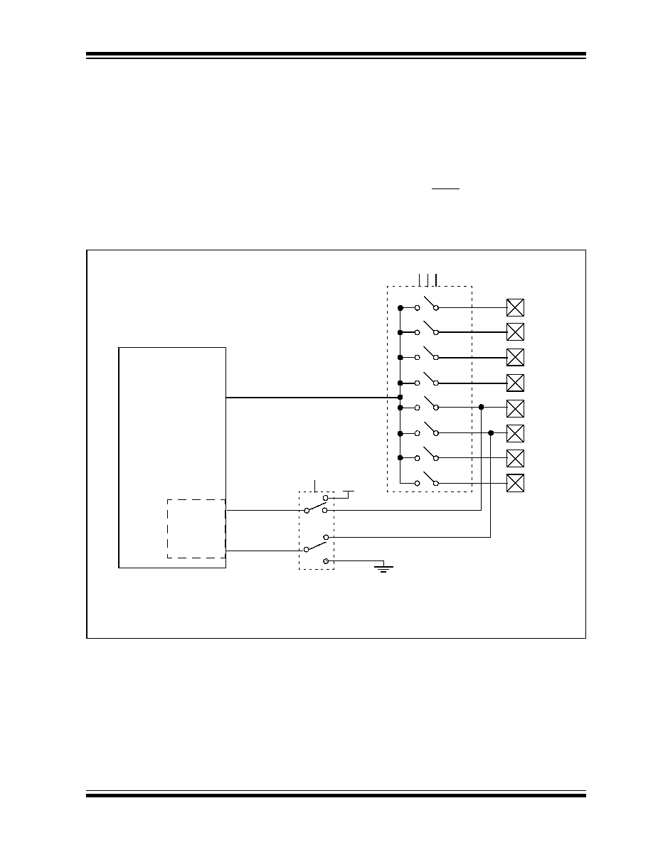
2002 Microchip Technology Inc.
Preliminary
DS41159B-page 239
PIC18FXX8
The analog reference voltage is software selectable to
either the device's positive and negative supply voltage
(V
DD
and V
SS
), or the voltage level on the
RA3/AN3/V
REF
+ pin and RA2/AN2/V
REF
- pin.
The A/D converter has a unique feature of being able
to operate while the device is in SLEEP mode. To oper-
ate in SLEEP, the A/D conversion clock must be
derived from the A/D's internal RC oscillator.
The output of the sample and hold is the input into the
converter, which generates the result via successive
approximation.
A device RESET forces all registers to their RESET
state. This forces the A/D module to be turned off and
any conversion is aborted.
Each port pin associated with the A/D converter can be
configured as an analog input (RA3 can also be a
voltage reference), or as a digital I/O.
The ADRESH and ADRESL registers contain the result
of the A/D conversion. When the A/D conversion is com-
plete, the result is loaded into the ADRESH/ADRESL
registers, the GO/DONE bit (ADCON0<2>) is cleared,
and A/D interrupt flag bit, ADIF, is set. The block
diagram of the A/D module is shown in Figure 20-1.
FIGURE 20-1:
A/D BLOCK DIAGRAM
(Input Voltage)
V
AIN
V
REF
+
Reference
voltage
V
DD
PCFG0
CHS2:CHS0
AN7
(1)
AN6
(1)
AN5
(1)
AN4
AN3
AN2
AN1
AN0
111
110
101
100
011
010
001
000
10-bit
Converter
V
REF
-
V
SS
A/D
Note 1: Channels AN5 through AN7 are not available on PIC18F2X8 devices.
2: All I/O pins have diode protection to V
DD
and V
SS
.
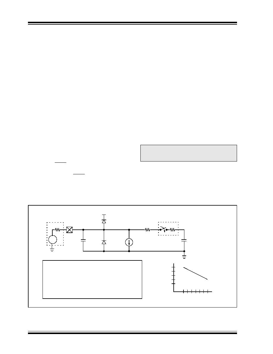
PIC18FXX8
DS41159B-page 240
Preliminary
2002 Microchip Technology Inc.
The value that is in the ADRESH/ADRESL registers is
not modified for a Power-on Reset. The
ADRESH/ADRESL registers will contain unknown data
after a Power-on Reset.
After the A/D module has been configured as desired,
the selected channel must be acquired before the con-
version is started. The analog input channels must
have their corresponding TRIS bits selected as an
input. To determine acquisition time, see Section 20.1.
After this acquisition time has elapsed, the A/D conver-
sion can be started. The following steps should be fol-
lowed for doing an A/D conversion:
1.
Configure the A/D module:
� Configure analog pins, voltage reference and
digital I/O (ADCON1)
� Select A/D input channel (ADCON0)
� Select A/D conversion clock (ADCON0)
� Turn on A/D module (ADCON0)
2.
Configure A/D interrupt (if desired):
� Clear ADIF bit
� Set ADIE bit
� Set GIE bit
3.
Wait the required acquisition time.
4.
Start conversion:
� Set GO/DONE bit (ADCON0)
5.
Wait for A/D conversion to complete, by either:
� Polling for the GO/DONE bit to be cleared
OR
� Waiting for the A/D interrupt
6.
Read A/D Result registers (ADRESH/ADRESL);
clear bit ADIF if required.
7.
For next conversion, go to step 1 or step 2, as
required. The A/D conversion time per bit is
defined as T
AD
. A minimum wait of 2 T
AD
is
required before next acquisition starts.
20.1
A/D Acquisition Requirements
For the A/D converter to meet its specified accuracy,
the charge holding capacitor (C
HOLD
) must be allowed
to fully charge to the input channel voltage level. The
analog input model is shown in Figure 20-2. The
source impedance (R
S
) and the internal sampling
switch (R
SS
) impedance directly affect the time
required to charge the capacitor C
HOLD
. The sampling
switch (R
SS
) impedance varies over the device voltage
(V
DD
). The source impedance affects the offset voltage
at the analog input (due to pin leakage current). The
maximum recommended impedance for analog
sources is 2.5 k
. After the analog input channel is
selected (changed), this acquisition must be done
before the conversion can be started.
FIGURE 20-2:
ANALOG INPUT MODEL
Note:
When the conversion is started, the hold-
ing capacitor is disconnected from the
input pin.
V
AIN
C
PIN
Rs
ANx
5 pF
V
DD
V
T
= 0.6V
V
T
= 0.6V
I
LEAKAGE
R
IC
1k
Sampling
Switch
SS
R
SS
C
HOLD
= 120 pF
V
SS
6V
Sampling Switch
5V
4V
3V
2V
5 6 7 8 9 10 11
(k
)
V
DD
� 500 nA
Legend: C
PIN
V
T
I
LEAKAGE
R
IC
SS
C
HOLD
= input capacitance
= threshold voltage
= leakage current at the pin due to
= interconnect resistance
= sampling switch
= sample/hold capacitance (from DAC)
various junctions

2002 Microchip Technology Inc.
Preliminary
DS41159B-page 241
PIC18FXX8
To calculate the minimum acquisition time,
Equation 20-1 may be used. This equation assumes
that 1/2 LSb error is used (1024 steps for the A/D). The
1/2 LSb error is the maximum error allowed for the A/D
to meet its specified resolution.
Example 20-1 shows the calculation of the minimum
required acquisition time T
ACQ
. This calculation is
based on the following application system assumptions:
� C
HOLD
=
120
pF
� Rs
=
2.5 k
� Conversion Error
1/2 LSb
� V
DD
=
5V
Rss = 7 k
� Temperature
=
50
�
C (system max.)
� V
HOLD
=
0V @ time = 0
EQUATION 20-1:
ACQUISITION TIME
EQUATION 20-2:
A/D MINIMUM CHARGING TIME
EXAMPLE 20-1:
CALCULATING THE MINIMUM REQUIRED ACQUISITION TIME
T
ACQ
=
Amplifier Settling Time + Holding Capacitor Charging Time + Temperature Coefficient
=
T
AMP
+ T
C
+ T
COFF
V
HOLD
=
(V
REF
� (V
REF
/2048)) � (1 - e
(-Tc/C
HOLD
(R
IC
+ R
SS
+ R
S
))
)
or
Tc
=
-(120 pF)(1 k
+ R
SS
+ R
S
) ln(1/2047)
T
ACQ
=
T
AMP
+ T
C
+ T
COFF
Temperature coefficient is only required for temperatures > 25
�C.
T
ACQ
=
2
�s + T
C
+ [(Temp - 25
�C)(0.05 �s/�C)]
T
C
=
-C
HOLD
(R
IC
+ R
SS
+ R
S
) ln(1/2047)
-120 pF (1 k
+ 7 k + 2.5 k) ln(0.0004885)
-120 pF (10.5 k
) ln(0.0004885)
-1.26
�s (-7.6241)
9.61
�s
T
ACQ
=
2
�s + 9.61 �s + [(50�C - 25�C)(0.05 �s/�C)]
11.61
�s + 1.25 �s
12.86
�s
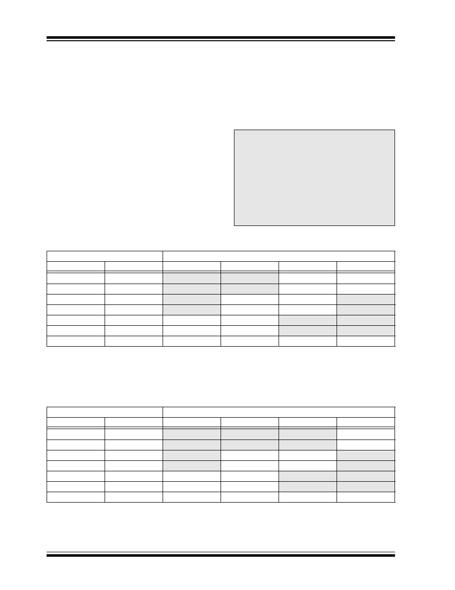
PIC18FXX8
DS41159B-page 242
Preliminary
2002 Microchip Technology Inc.
20.2
Selecting the A/D Conversion Clock
The A/D conversion time per bit is defined as T
AD
. The
A/D conversion requires 12 T
AD
per 10-bit conversion.
The source of the A/D conversion clock is software
selectable. The seven possible options for T
AD
are:
� 2 T
OSC
� 4 T
OSC
� 8 T
OSC
� 16 T
OSC
� 32 T
OSC
� 64 T
OSC
� Internal RC oscillator.
For correct A/D conversions, the A/D conversion clock
(T
AD
) must be selected to ensure a minimum T
AD
time
of 1.6
�
s.
Table 20-1 shows the resultant T
AD
times derived from
the device operating frequencies and the A/D clock
source selected.
20.3
Configuring Analog Port Pins
The ADCON1, TRISA and TRISE registers control the
operation of the A/D port pins. The port pins that are
desired as analog inputs must have their corresponding
TRIS bits set (input). If the TRIS bit is cleared (output),
the digital output level (V
OH
or V
OL
) will be converted.
The A/D operation is independent of the state of the
CHS2:CHS0 bits and the TRIS bits.
TABLE 20-1:
T
AD
vs. DEVICE OPERATING FREQUENCIES
TABLE 20-2:
T
AD
vs. DEVICE OPERATING FREQUENCIES (FOR EXTENDED, LC DEVICES)
Note 1: When reading the port register, all pins con-
figured as analog input channels will read
as cleared (a low level). Pins configured as
digital inputs will convert an analog input.
Analog levels on a digitally configured input
will not affect the conversion accuracy.
2: Analog levels on any pin that is defined as
a digital input (including the AN4:AN0
pins) may cause the input buffer to con-
sume current that is out of the devices
specification.
AD Clock Source (T
AD
)
Device Frequency
Operation
ADCS2:ADCS0
20 MHz
5 MHz
1.25 MHz
333.33 kHz
2 T
OSC
000
100 ns
(2)
400 ns
(2)
1.6
�
s
6
�
s
4 T
OSC
100
200 ns
(2)
800 ns
(2)
3.2
�
s
12
�
s
8 T
OSC
001
400 ns
(2)
1.6
�
s
6.4
�
s
24
�
s
(3)
16 T
OSC
101
800 ns
(2)
3.2
�
s
12.8
�
s
48
�
s
(3)
32 T
OSC
010
1.6
�
s
6.4
�
s
25.6
�
s
(3)
96
�
s
(3)
64 T
OSC
110
3.2
�
s
12.8
�
s
51.2
�
s
(3)
192
�
s
(3)
RC
011
2 - 6
�
s
(1)
2 - 6
�
s
(1)
2 - 6
�
s
(1)
2 - 6
�
s
(1)
Legend: Shaded cells are outside of recommended range.
Note 1: The RC source has a typical T
AD
time of 4
�
s.
2: These values violate the minimum required T
AD
time.
3: For faster conversion times, the selection of another clock source is recommended.
AD Clock Source (T
AD
)
Device Frequency
Operation
ADCS2:ADCS0
4 MHz
2 MHz
1.25 MHz
333.33 kHz
2 T
OSC
000
500 ns
(2)
1.0
�
s
(2)
1.6
�
s
(2)
6
�
s
4 T
OSC
100
1.0
�
s
(2)
2.0
�
s
(2)
3.2
�
s
(2)
12
�
s
8 T
OSC
001
2.0
�
s
(2)
4.0
�
s
6.4
�
s
24
�
s
(3)
16 T
OSC
101
4.0
�
s
(2)
8.0
�
s
12.8
�
s
48
�
s
(3)
32 T
OSC
010
8.0
�
s
16.0
�
s
25.6
�
s
(3)
96
�
s
(3)
64 T
OSC
110
16.0
�
s
32.0
�
s
51.2
�
s
(3)
192
�
s
(3)
RC
011
3 - 9
�
s
(1,4)
3 - 9
�
s
(1,4)
3 - 9
�
s
(1,4)
3 - 9
�
s
(1,4)
Legend: Shaded cells are outside of recommended range.
Note 1: The RC source has a typical T
AD
time of 6
�
s.
2: These values violate the minimum required T
AD
time.
3: For faster conversion times, the selection of another clock source is recommended.
2002 Microchip Technology Inc.
Preliminary
DS41159B-page 243
PIC18FXX8
20.4
A/D Conversions
Figure 20-3 shows the operation of the A/D converter
after the GO bit has been set. Clearing the GO/DONE
bit during a conversion will abort the current conver-
sion. The A/D result register pair will NOT be updated
with the partially completed A/D conversion sample.
That is, the ADRESH:ADRESL registers will continue
to contain the value of the last completed conversion
(or the last value written to the ADRESH:ADRESL reg-
isters). After the A/D conversion is aborted, a 2 T
AD
wait
is required before the next acquisition is started. After
this 2 T
AD
wait, acquisition on the selected channel is
automatically started.
20.5
Use of the ECCP Trigger
An A/D conversion can be started by the "special event
trigger" of the ECCP module. This requires that the
ECCP1M3:ECCP1M0 bits (ECCP1CON<3:0>) be pro-
grammed as
1011
and that the A/D module is enabled
(ADON bit is set). When the trigger occurs, the
GO/DONE bit will be set, starting the A/D conversion and
the Timer1 (or Timer3) counter will be reset to zero.
Timer1 (or Timer3) is reset to automatically repeat the
A/D acquisition period with minimal software overhead
(moving ADRESH/ADRESL to the desired location). The
appropriate analog input channel must be selected and
the minimum acquisition done before the "special event
trigger" sets the GO/DONE bit (starts a conversion).
If the A/D module is not enabled (ADON is cleared), the
"special event trigger" will be ignored by the A/D module,
but will still reset the Timer1 (or Timer3) counter.
FIGURE 20-3:
A/D CONVERSION T
AD
CYCLES
TABLE 20-3:
SUMMARY OF A/D REGISTERS
Note:
The GO/DONE bit should NOT be set in
the same instruction that turns on the A/D.
Name
Bit 7
Bit 6
Bit 5
Bit 4
Bit 3
Bit 2
Bit 1
Bit 0
Value on
POR, BOR
Value on
all other
RESETS
INTCON
GIE/GIEH
PEIE/GIEL
TMR0IE
INT0IE
RBIE
TMR0IF
INT0IF
RBIF
0000 000x
0000 000u
PIR1
PSPIF
(1)
ADIF
RCIF
TXIF
SSPIF
CCP1IF
TMR2IF
TMR1IF
0000 0000
0000 0000
PIE1
PSPIE
(1)
ADIE
RCIE
TXIE
SSPIE
CCP1IE
TMR2IE
TMR1IE
0000 0000
0000 0000
IPR1
PSPIP
(1)
ADIP
RCIP
TXIP
SSPIP
CCP1IP
TMR2IP
TMR1IP
0000 0000
0000 0000
PIR2
--
CMIF
(1)
--
EEIF
BCLIF
LVDIF
TMR3IF
ECCP1IF
(1)
-0-0 0000
-0-0 0000
PIE2
--
CMIE
(1)
--
EEIE
BCLIE
LVDIE
TMR3IE
ECCP1IE
(1)
-0-0 0000
-0-0 0000
IPR2
--
CMIP
(1)
--
EEIP
BCLIP
LVDIP
TMR3IP
ECCP1IP
(1)
-0-0 0000
-0-0 0000
ADRESH A/D Result Register
xxxx xxxx
uuuu uuuu
ADRESL A/D Result Register
xxxx xxxx
uuuu uuuu
ADCON0
ADCS1
ADCS0
CHS2
CHS1
CHS0
GO/DONE
--
ADON
0000 00-0
0000 00-0
ADCON1
ADFM
ADCS2
--
--
PCFG3
PCFG2
PCFG1
PCFG0
00-- 0000
00-- 0000
PORTA
--
RA6
RA5
RA4
RA3
RA2
RA1
RA0
-00x 0000
-00u 0000
TRISA
--
PORTA Data Direction Register
-111 1111
-111 1111
PORTE
--
--
--
--
--
RE2
RE1
RE0
---- -000
---- -000
LATE
--
--
--
--
--
LATE2
LATE1
LATE0
---- -xxx
---- -uuu
TRISE
IBF
OBF
IBOV
PSPMODE
--
TRISE2
TRISE1
TRISE0
0000 -111
0000 -111
Legend: x = unknown, u = unchanged, - = unimplemented, read as '0'. Shaded cells are not used for A/D conversion.
Note
1: These bits are reserved on PIC18F2X8 devices; always maintain these bits clear.
T
AD
1 T
AD
2 T
AD
3 T
AD
4 T
AD
5 T
AD
6 T
AD
7 T
AD
8
T
AD
11
Set GO bit
Holding capacitor is disconnected from analog input
b9
b8
b7
b6
b5
b4
b3
b2
T
AD
9 T
AD
10
b1
b0
T
CY
- T
AD
Next Q4: ADRESH/ADRESL is loaded, GO bit is cleared,
ADIF bit is set, holding capacitor is connected to analog input.
Conversion Starts
b0
(typically 100 ns)

PIC18FXX8
DS41159B-page 244
Preliminary
2002 Microchip Technology Inc.
NOTES:

2002 Microchip Technology Inc.
Preliminary
DS41159B-page 245
PIC18FXX8
21.0
COMPARATOR MODULE
The comparator module contains two analog compara-
tors. The inputs to the comparators are multiplexed
with the RD0 through RD3 pins. The On-Chip Voltage
Reference (Section 22.0) can also be an input to the
comparators.
The CMCON register, shown in Register 21-1, controls
the comparator input and output multiplexers. A block
diagram of the comparator is shown in Figure 21-1.
REGISTER 21-1:
CMCON REGISTER
Note:
The analog comparators are only available
on the PIC18F448 and PIC18F458.
R-0
R-0
R/W-0
R/W-0
R/W-0
R/W-0
R/W-0
R/W-0
C2OUT
C1OUT
C2INV
C1INV
CIS
CM2
CM1
CM0
bit 7
bit 0
bit 7
C2OUT: Comparator 2 Output bit
When C2INV = 0:
1
= C2 V
IN
+ > C2 V
IN
�
0
= C2 V
IN
+ < C2 V
IN
�
When C2INV = 1:
1
= C2 V
IN
+ < C2 V
IN
�
0
= C2 V
IN
+ > C2 V
IN
�
bit 6
C1OUT: Comparator 1 Output bit
When C1INV = 0:
1
= C1 V
IN
+ > C1 V
IN
�
0
= C1 V
IN
+ < C1 V
IN
�
When C1INV = 1:
1
= C1 V
IN
+ < C1 V
IN
�
0
= C1 V
IN
+ > C1 V
IN
�
bit 5
C2INV: Comparator 2 Output Inversion bit
1
= C2 output inverted
0
= C2 output not inverted
bit 4
C1INV: Comparator 1 Output Inversion bit
1
= C1 output inverted
0
= C1 output not inverted
bit 3
CIS: Comparator Input Switch bit
When CM2:CM0 =
110
:
1
= C1 V
IN
- connects to RD0/PSP0
C2 V
IN
- connects to RD2/PSP2
0
= C1 V
IN
- connects to RD1/PSP1
C2 V
IN
- connects to RD3/PSP3
bit 2-0
CM2:CM0: Comparator Mode bits
Figure 21-1 shows the Comparator modes and CM2:CM0 bit settings
Legend:
R = Readable bit
W = Writable bit
U = Unimplemented bit, read as `0'
- n = Value at POR
'1' = Bit is set
'0' = Bit is cleared
x = Bit is unknown
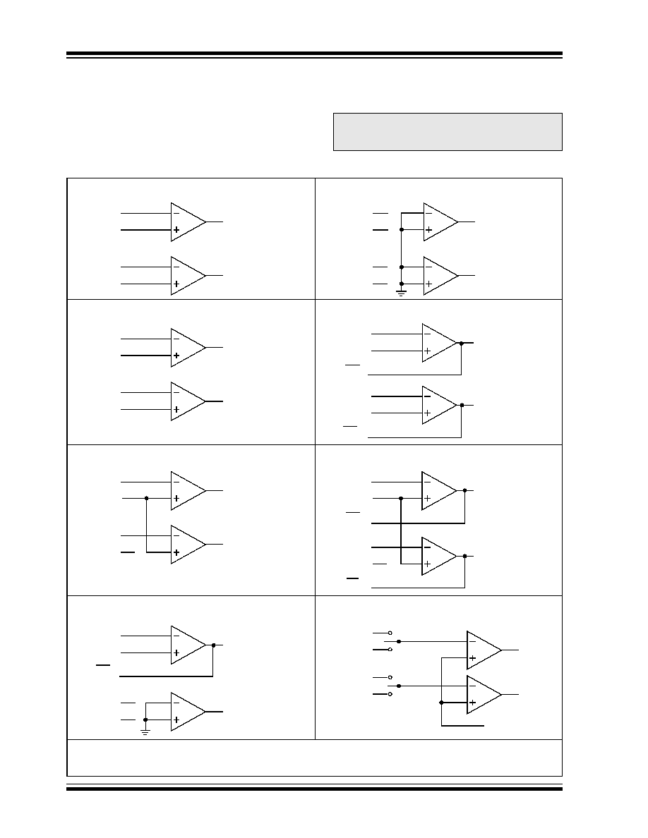
PIC18FXX8
DS41159B-page 246
Preliminary
2002 Microchip Technology Inc.
21.1
Comparator Configuration
There are eight modes of operation for the compara-
tors. The CMCON register is used to select these
modes. Figure 21-1 shows the eight possible modes.
The TRISD register controls the data direction of the
comparator pins for each mode. If the Comparator
mode is changed, the comparator output level may not
be valid for the specified mode change delay, shown in
Electrical Specifications (Section 27.0).
FIGURE 21-1:
COMPARATOR I/O OPERATING MODES
Note:
Comparator interrupts should be disabled
during a Comparator mode change.
Otherwise, a false interrupt may occur.
C1
RD1/PSP1
V
IN
-
V
IN
+
Off
(Read as '0')
Comparators Reset (POR Default Value)
A
A
CM2:CM0 =
000
C2
RD3/PSP3
V
IN
-
V
IN
+
RD2/PSP2
Off
(Read as '0')
A
A
C1
RD1/PSP1
V
IN
-
V
IN
+
RD0/PSP0
C1OUT
Two Independent Comparators
A
A
CM2:CM0 =
010
C2
RD3/PSP3
V
IN
-
V
IN
+
RD2/PSP2
C2OUT
A
A
C1
RD1/PSP1
V
IN
-
V
IN
+
RD0/PSP0
C1OUT
Two Common Reference Comparators
A
A
CM2:CM0 =
100
C2
RD3/PSP3
V
IN
-
V
IN
+
RD2/PSP2
C2OUT
A
D
C2
RD3/PSP3
V
IN
-
V
IN
+
RD2/PSP2
Off
(Read as '0')
One Independent Comparator with Output
D
D
CM2:CM0 =
001
C1
RD1/PSP1
V
IN
-
V
IN
+
RD0/PSP0
C1OUT
A
A
C1
RD1/PSP1
V
IN
-
V
IN
+
RD0/PSP0
Off
(Read as '0')
Comparators Off
D
D
CM2:CM0 =
111
C2
RD3/PSP3
V
IN
-
V
IN
+
RD2/PSP2
Off
(Read as '0')
D
D
C1
RD1/PSP1
V
IN
-
V
IN
+
RD0/PSP0
C1OUT
Four Inputs Multiplexed to Two Comparators
A
A
CM2:CM0 =
110
C2
RD3/PSP3
V
IN
-
V
IN
+
RD2/PSP2
C2OUT
A
A
From V
REF
Module
CIS = 0
CIS = 1
CIS = 0
CIS = 1
C1
RD1/PSP1
V
IN
-
V
IN
+
RD0/PSP0
C1OUT
Two Common Reference Comparators with Outputs
A
A
CM2:CM0 =
101
C2
RD3/PSP3
V
IN
-
V
IN
+
RD2/PSP2
C2OUT
A
D
A = Analog Input, port reads zeros always
D = Digital Input
CIS (CMCON<3>) is the Comparator Input Switch
CV
REF
C1
RD1/PSP1
V
IN
-
V
IN
+
RD0/PSP0
C1OUT
Two Independent Comparators with Outputs
A
A
CM2:CM0 =
011
C2
RD3/PSP3
V
IN
-
V
IN
+
RD2/PSP2
C2OUT
A
A
RE1/WR/AN6
RE2/CS/AN7
RE1/WR/AN6
RE2/CS/AN7
RE1/WR/AN6
RD0/PSP0
2002 Microchip Technology Inc.
Preliminary
DS41159B-page 247
PIC18FXX8
21.2
Comparator Operation
A single comparator is shown in Figure 21-2 along with
the relationship between the analog input levels and
the digital output. When the analog input at V
IN
+ is less
than the analog input V
IN
-, the output of the comparator
is a digital low level. When the analog input at V
IN
+ is
greater than the analog input V
IN
-, the output of the
comparator is a digital high level. The shaded areas of
the output of the comparator in Figure 21-2 represent
the uncertainty due to input offsets and response time.
21.3
Comparator Reference
An external or internal reference signal may be used
depending on the Comparator Operating mode. The
analog signal present at V
IN
- is compared to the signal
at V
IN
+, and the digital output of the comparator is
adjusted accordingly (Figure 21-2).
FIGURE 21-2:
SINGLE COMPARATOR
21.3.1
EXTERNAL REFERENCE SIGNAL
When external voltage references are used, the
comparator module can be configured to have the com-
parators operate from the same, or different reference
sources. However, threshold detector applications may
require the same reference. The reference signal must
be between V
SS
and V
DD
, and can be applied to either
pin of the comparator(s).
21.3.2
INTERNAL REFERENCE SIGNAL
The comparator module also allows the selection of an
internally generated voltage reference for the compara-
tors. Section 22.0 contains a detailed description of the
Comparator Voltage Reference Module that provides
this signal. The internal reference signal is used when
comparators are in mode CM<2:0> =
110
(Figure 21-1).
In this mode, the internal voltage reference is applied to
the V
IN
+ pin of both comparators.
21.4
Comparator Response Time
Response time is the minimum time, after selecting a
new reference voltage or input source, before the
comparator output has a valid level. If the internal ref-
erence is changed, the maximum delay of the internal
voltage reference must be considered when using the
comparator outputs. Otherwise the maximum delay of
the comparators should be used (Section 27.0).
21.5
Comparator Outputs
The comparator outputs are read through the CMCON
register. These bits are read only. The comparator
outputs may also be directly output to the RE1 and RE2
I/O pins. When enabled, multiplexors in the output path
of the RE1 and RE2 pins will switch and the output of
each pin will be the unsynchronized output of the com-
parator. The uncertainty of each of the comparators is
related to the input offset voltage and the response time
given in the specifications. Figure 21-3 shows the
comparator output block diagram.
The TRISE bits will still function as an output enable/
disable for the RE1 and RE2 pins while in this mode.
The polarity of the comparator outputs can be changed
using the C2INV and C1INV bits (CMCON<4:5>).
-
+
V
IN
+
V
IN
-
Output
V
IN�
V
IN+
utput
Output
V
IN
+
V
IN
-
Note 1: When reading the PORT register, all pins
configured as analog inputs will read as a
`0'. Pins configured as digital inputs will
convert an analog input, according to the
Schmitt Trigger input specification.
2: Analog levels on any pin defined as a dig-
ital input, may cause the input buffer to
consume more current than is specified.
PIC18FXX8
DS41159B-page 248
Preliminary
2002 Microchip Technology Inc.
FIGURE 21-3:
COMPARATOR OUTPUT BLOCK DIAGRAM
21.6
Comparator Interrupts
The comparator interrupt flag is set whenever there is
a change in the output value of either comparator.
Software will need to maintain information about the
status of the output bits, as read from CMCON<7:6>, to
determine the actual change that occurred. The CMIF
bit (PIR registers) is the comparator interrupt flag. The
CMIF bit must be reset by clearing `0'. Since it is also
possible to write a '1' to this register, a simulated
interrupt may be initiated.
The CMIE bit (PIE registers) and the PEIE bit (INTCON
register) must be set to enable the interrupt. In addition,
the GIE bit must also be set. If any of these bits are
clear, the interrupt is not enabled, though the CMIF bit
will still be set if an interrupt condition occurs.
.
The user, in the Interrupt Service Routine, can clear the
interrupt in the following manner:
a)
Any read or write of CMCON will end the
mismatch condition.
b)
Clear flag bit CMIF.
A mismatch condition will continue to set flag bit CMIF.
Reading CMCON will end the mismatch condition and
allow flag bit CMIF to be cleared.
D
Q
EN
To RE1 or
RE2 pin
Bus
Data
Read CMCON
Set
MULTIPLEX
CMIF
bit
-
+
D
Q
EN
CL
Port Pins
Read CMCON
RESET
From
Other
Comparator
CxINV
Note:
If a change in the CMCON register
(C1OUT or C2OUT) should occur when a
read operation is being executed (start of
the Q2 cycle), then the CMIF (PIR
registers) interrupt flag may not get set.
2002 Microchip Technology Inc.
Preliminary
DS41159B-page 249
PIC18FXX8
21.7
Comparator Operation During
SLEEP
When a comparator is active and the device is placed
in SLEEP mode, the comparator remains active and
the interrupt is functional, if enabled. This interrupt will
wake-up the device from SLEEP mode, when enabled.
While the comparator is powered up, higher SLEEP
currents than shown in the power-down current
specification will occur. Each operational comparator
will consume additional current, as shown in the com-
parator specifications. To minimize power consumption
while in SLEEP mode, turn off the comparators,
CM<2:0> =
111
, before entering SLEEP. If the device
wakes up from SLEEP, the contents of the CMCON
register are not affected.
21.8
Effects of a RESET
A device RESET forces the CMCON register to its
RESET state, causing the comparator module to be in
the comparator RESET mode, CM<2:0> =
000
. This
ensures that all potential inputs are analog inputs.
Device current is minimized when analog inputs are
present at RESET time. The comparators will be
powered down during the RESET interval.
21.9
Analog Input Connection
Considerations
A simplified circuit for an analog input is shown in
Figure 21-4. Since the analog pins are connected to a
digital output, they have reverse biased diodes to V
DD
and V
SS
. The analog input, therefore, must be between
V
SS
and V
DD
. If the input voltage deviates from this
range by more than 0.6V in either direction, one of the
diodes is forward biased and a latchup condition may
occur. A maximum source impedance of 10 k
is rec-
ommended for the analog sources. Any external com-
ponent connected to an analog input pin, such as a
capacitor or a Zener diode, should have very little
leakage current.
FIGURE 21-4:
ANALOG INPUT MODEL
VA
R
S
<
10k
A
IN
C
PIN
5 pF
V
DD
V
T
= 0.6V
V
T
= 0.6V
R
IC
I
LEAKAGE
�
500 nA
V
SS
Legend:
C
PIN
=
Input Capacitance
V
T
= Threshold
Voltage
I
LEAKAGE
=
Leakage Current at the pin due to various junctions
R
IC
=
Interconnect Resistance
R
S
=
Source Impedance
VA
=
Analog Voltage

PIC18FXX8
DS41159B-page 250
Preliminary
2002 Microchip Technology Inc.
TABLE 21-1:
REGISTERS ASSOCIATED WITH COMPARATOR MODULE
Name
Bit 7
Bit 6
Bit 5
Bit 4
Bit 3
Bit 2
Bit 1
Bit 0
Value on
POR
Value on
all other
RESETS
CMCON
C2OUT C1OUT C2INV
C1INV
CIS
CM2
CM1
CM0
0000 0000 0000 0000
CVRCON CVREN CVROE CVRR
CVRSS
CVR3
CVR2
CVR1
CVR0
0000 0000 0000 0000
INTCON
GIE/
GIEH
PEIE/
GIEL
TMR0IE
INT0IE
RBIE
TMR0IF INT0IF
RBIF
0000 000x 0000 000u
PIR2
--
CMIF
(1)
--
EEIF
BCLIF
LVDIF
TMR3IF ECCP1IF
(1)
-0-0 0000 -0-0 0000
PIE2
--
CMIE
(1)
--
EEIE
BCLIE
LVDIE
TMR3IE ECCP1IE
(1)
-0-0 0000 -0-0 0000
IPR2
--
CMIP
(1)
--
EEIP
BCLIP
LVDIP
TMR3IP ECCP1IP
(1)
-1-1 1111 -1-1 1111
PORTD
RD7
RD6
RD5
RD4
RD3
RD2
RD1
RD0
x000 0000 u000 0000
LATD
LATD7
LATD6
LATD5
LATD4
LATD3
LATD2
LATD1
LATD0
xxxx xxxx uuuu uuuu
TRISD
PORTD Data Direction Register
1111 1111 1111 1111
PORTE
--
--
--
--
--
RE2
RE1
RE0
---- -000 ---- -000
LATE
--
--
--
--
--
LATE2
LATE1
LATE0
---- -xxx ---- -uuu
TRISE
IBF
(1)
OBF
(1)
IBOV
(1)
PSPMODE
(1)
--
TRISE2 TRISE1
TRISE0
0000 -111 0000 -111
Legend:
x
= unknown,
u
= unchanged, - = unimplemented, read as "0"
Note 1: These bits are reserved on PIC18F2X8 devices; always maintain these bits clear.

2002 Microchip Technology Inc.
Preliminary
DS41159B-page 251
PIC18FXX8
22.0
COMPARATOR VOLTAGE
REFERENCE MODULE
This module is a 16-tap resistor ladder network that
provides a selectable voltage reference. The resistor
ladder is segmented to provide two ranges of CV
REF
values and has a power-down function to conserve
power when the reference is not being used. The
CVRCON register controls the operation of the
reference as shown in Register 22-1. The block
diagram is shown in Figure 22-1.
The comparator and reference supply voltage can
come from either V
DD
and V
SS
, or the external V
REF
+
and V
REF
-, that are multiplexed with RA3 and RA2. The
comparator reference supply voltage is controlled by
the CVRSS bit.
22.1
Configuring the Comparator
Voltage Reference
The Comparator Voltage Reference can output 16 dis-
tinct voltage levels for each range. The equations used
to calculate the output of the Comparator Voltage
Reference are as follows.
EQUATION 22-1:
EQUATION 22-2:
The settling time of the Comparator Voltage Reference
must be considered when changing the RA0/AN0/CV
REF
output (see Table 27-4 in Section 27.2).
REGISTER 22-1:
CVRCON REGISTER
Note:
The Comparator Voltage Reference is only
available on the PIC18F448 and
PIC18F458.
If CVRR = 1:
CV
REF
= (CVR<3:0>/24) x CV
RSRC
where:
CVRSS = 1, CV
RSRC
= (V
REF
+) � (V
REF
-)
CVRSS = 0, CV
RSRC
= V
DD
� V
SS
If CVRR = 0:
CV
REF
= (CV
RSRC
x 1/4) + (CVR<3:0>/32) x CV
RSRC
where:
CVRSS = 1, CV
RSRC
= (V
REF
+) � (V
REF
-)
CVRSS = 0, CV
RSRC
= V
DD
� V
SS
R/W-0
R/W-0
R/W-0
R/W-0
R/W-0
R/W-0
R/W-0
R/W-0
CVREN
CVROE
CVRR
CVRSS
CVR3
CVR2
CVR1
CVR0
bit 7
bit 0
bit 7
CVREN: Comparator Voltage Reference Enable bit
1
= CV
REF
circuit powered on
0
= CV
REF
circuit powered down
bit 6
CVROE: Comparator V
REF
Output Enable bit
1
= CV
REF
voltage level is also output on the RA0/AN0/CV
REF
pin
0
= CV
REF
voltage is disconnected from the RA0/AN0/CV
REF
pin
bit 5
CVRR: Comparator V
REF
Range Selection bit
1
= 0.00 CV
RSRC
to 0.625 CV
RSRC
, with CV
RSRC
/24 step size
0
= 0.25 CV
RSRC
to 0.719 CV
RSRC
, with CV
RSRC
/32 step size
bit 4
CVRSS: Comparator V
REF
Source Selection bit
1
= Comparator reference source CV
RSRC
= V
DD
� V
SS
0
= Comparator reference source CV
RSRC
= (V
REF
+) � (V
REF
-)
bit 3-0
CVR<3:0>: Comparator V
REF
Value Selection 0
CVR3:CVR0
15 bits
When CVRR = 1:
CV
REF
= (CVR3:CVR0/24)
�
(CV
RSRC
)
When CVRR = 0:
CV
REF
= 1/4
�
(CV
RSRC
) + (CVR3:CVR0/32)
�
(CV
RSRC
)
Legend:
R = Readable bit
W = Writable bit
U = Unimplemented bit, read as `0'
- n = Value at POR
'1' = Bit is set
'0' = Bit is cleared
x = Bit is unknown
PIC18FXX8
DS41159B-page 252
Preliminary
2002 Microchip Technology Inc.
FIGURE 22-1:
VOLTAGE REFERENCE BLOCK DIAGRAM
22.2
Voltage Reference Accuracy/Error
The full range of voltage reference cannot be realized
due to the construction of the module. The transistors
on the top and bottom of the resistor ladder network
(Figure 22-1) keep V
REF
from approaching the refer-
ence source rails. The voltage reference is derived
from the reference source; therefore, the V
REF
output
changes with fluctuations in that source. The absolute
accuracy of the voltage reference can be found in
Section 27.0.
22.3
Operation During SLEEP
When the device wakes up from SLEEP through an
interrupt or a Watchdog Timer Time-out, the contents of
the CVRCON register are not affected. To minimize
current consumption in SLEEP mode, the voltage
reference should be disabled.
22.4
Effects of a RESET
A device RESET disables the voltage reference by
clearing bit CVREN (CVRCON register). This RESET
also disconnects the reference from the RA2 pin by
clearing bit CVROE (CVRCON register) and selects
the high voltage range by clearing bit CVRR (CVRCON
register). The CVRSS value select bits, CVRCON<3:0>,
are also cleared.
22.5
Connection Considerations
The voltage reference module operates independently
of the comparator module. The output of the reference
generator may be connected to the RA0/AN0 pin if the
TRISA<0> bit is set and the CVROE bit (CVRCON<6>)
is set. Enabling the voltage reference output onto the
RA0/AN0 pin, with an input signal present, will increase
current consumption. Connecting RA0/AN0 as a digital
output with CVRSS enabled, will also increase current
consumption.
The RA0/AN0 pin can be used as a simple D/A output
with limited drive capability. Due to the limited current
drive capability, a buffer must be used on the voltage
reference output for external connections to V
REF
.
Figure 22-2 shows an example buffering technique.
CVRR
8R
CVR3
CVR0
(From CVRCON<3:0>)
16-to-1 Analog MUX
8R
R
R
R
R
RA0/AN0/CV
REF
16 Stages
CVRSS = 0
V
DD
V
REF
+
CVRSS = 0
CVRSS = 1
RA2/AN2V
REF
-
CVRSS = 1
or CV
REF
of Comparator
CVREN
2002 Microchip Technology Inc.
Preliminary
DS41159B-page 253
PIC18FXX8
FIGURE 22-2:
VOLTAGE REFERENCE OUTPUT BUFFER EXAMPLE
TABLE 22-1:
REGISTERS ASSOCIATED WITH COMPARATOR VOLTAGE REFERENCE
CV
REF
Output
+
�
�
�
CV
REF
Module
Voltage
Reference
Output
Impedance
R
(1)
RA0/AN0
Note 1: R is dependent upon the voltage reference configuration CVRCON<3:0> and CVRCON<5>.
Name
Bit 7
Bit 6
Bit 5
Bit 4
Bit 3
Bit 2
Bit 1
Bit 0
Value on
POR
Value on
all other
RESETS
CVRCON
CVREN CVROE
CVRR
CVRSS
CVR3
CVR2
CVR1
CVR0
0000 0000 0000 0000
CMCON
C2OUT
C1OUT
C2INV
C1INV
CIS
CM2
CM1
CM0
0000 0000 0000 0000
TRISA
--
TRISA6 TRISA5 TRISA4 TRISA3
TRISA2
TRISA1 TRISA0
-111 1111 -111 1111
Legend:
x
= unknown,
u
= unchanged, - = unimplemented, read as "0".
Shaded cells are not used with the comparator voltage reference.

PIC18FXX8
DS41159B-page 254
Preliminary
2002 Microchip Technology Inc.
NOTES:
2002 Microchip Technology Inc.
Preliminary
DS41159B-page 255
PIC18FXX8
23.0
LOW VOLTAGE DETECT
In many applications, the ability to determine if the
device voltage (V
DD
) is below a specified voltage level
is a desirable feature. A window of operation for the
application can be created, where the application soft-
ware can do "housekeeping tasks" before the device
voltage exits the valid operating range. This can be
done using the Low Voltage Detect module.
This module is a software programmable circuitry,
where a device voltage trip point can be specified.
When the voltage of the device becomes lower than the
specified point, an interrupt flag is set. If the interrupt is
enabled, the program execution will branch to the inter-
rupt vector address and the software can then respond
to that interrupt source.
The Low Voltage Detect circuitry is completely under
software control. This allows the circuitry to be "turned
off" by the software, which minimizes the current
consumption for the device.
Figure 23-1 shows a possible application voltage curve
(typically for batteries). Over time, the device voltage
decreases. When the device voltage equals voltage V
A
,
the LVD logic generates an interrupt. This occurs at
time T
A
. The application software then has the time,
until the device voltage is no longer in valid operating
range, to shutdown the system. Voltage point V
B
is the
minimum valid operating voltage specification. This
occurs at time T
B
. The difference T
B
� T
A
is the total
time for shutdown.
The block diagram for the LVD module is shown in
Figure 23-2. A comparator uses an internally gener-
ated reference voltage as the set point. When the
selected tap output of the device voltage crosses the
set point (is lower than), the LVDIF bit is set.
Each node in the resistor divider represents a "trip
point" voltage. The "trip point" voltage is the minimum
supply voltage level at which the device can operate
before the LVD module asserts an interrupt. When the
supply voltage is equal to the trip point, the voltage
tapped off of the resistor array is equal to the internal
reference voltage generated by the voltage reference
module. The comparator then generates an interrupt
signal setting the LVDIF bit. This voltage is software
programmable to any one of 16 values (see
Figure 23-2). The trip point is selected by programming
the LVDL3:LVDL0 bits (LVDCON<3:0>).
FIGURE 23-1:
TYPICAL LOW VOLTAGE DETECT APPLICATION
Time
Vo
l
t
a
g
e
V
A
V
B
T
A
T
B
V
A
= LVD trip point
V
B
= Minimum valid device
operating voltage
Legend:
PIC18FXX8
DS41159B-page 256
Preliminary
2002 Microchip Technology Inc.
FIGURE 23-2:
LOW VOLTAGE DETECT (LVD) BLOCK DIAGRAM
The LVD module has an additional feature that allows
the user to supply the trip voltage to the module from
an external source. This mode is enabled when bits
LVDL3:LVDL0 are set to `
1111
'. In this state, the com-
parator input is multiplexed from the external input pin
LVDIN to one input of the comparator (Figure 23-3).
The other input is connected to the internally gener-
ated voltage reference (parameter D423 in
Section 27.2). This gives users flexibility, because it
allows them to configure the Low Voltage Detect inter-
rupt to occur at any voltage in the valid operating
range.
FIGURE 23-3:
LOW VOLTAGE DETECT (LVD) WITH EXTERNAL INPUT BLOCK DIAGRAM
LVDIF
V
DD
16 t
o
1
MUX
LVDEN
LVDCON
Internally Generated
Reference Voltage
LVDIN
LVD3:LVD0
Register
LVD
EN
16 t
o
1
M
U
X
BGAP
BODEN
LVDEN
VxEN
LVDIN
V
DD
V
DD
Externally Generated
Trip Point
LVD3:LVD0
LVDCON
Register

2002 Microchip Technology Inc.
Preliminary
DS41159B-page 257
PIC18FXX8
23.1
Control Register
The Low Voltage Detect Control register controls the
operation of the Low Voltage Detect circuitry.
REGISTER 23-1:
LVDCON REGISTER
U-0
U-0
R-0
R/W-0
R/W-0
R/W-1
R/W-0
R/W-1
--
--
IRVST
LVDEN
LVDL3
LVDL2
LVDL1
LVDL0
bit 7
bit 0
bit 7-6
Unimplemented: Read as '0'
bit 5
IRVST: Internal Reference Voltage Stable Flag bit
1
= Indicates that the Low Voltage Detect logic will generate the interrupt flag at the
specified voltage range
0
= Indicates that the Low Voltage Detect logic will not generate the interrupt flag at the
specified voltage range and the LVD interrupt should not be enabled
bit 4
LVDEN: Low Voltage Detect Power Enable bit
1
= Enables LVD, powers up LVD circuit
0
= Disables LVD, powers down LVD circuit
bit 3-0
LVDL3:LVDL0: Low Voltage Detection Limit bits
1111
= External analog input is used (input comes from the LVDIN pin)
1110
= 4.5V min. - 4.77V max.
1101
= 4.2V min. - 4.45V max.
1100
= 4.0V min. - 4.24V max.
1011
= 3.8V min. - 4.03V max.
1010
= 3.6V min. - 3.82V max.
1001
= 3.5V min. - 3.71V max.
1000
= 3.3V min. - 3.50V max.
0111
= 3.0V min. - 3.18V max.
0110
= 2.8V min. - 2.97V max.
0101
= 2.7V min. - 2.86V max.
0100
= 2.5V min. - 2.65V max.
0011
= 2.4V min. - 2.54V max.
0010
= 2.2V min. - 2.33V max.
0001
= 2.0V min. - 2.12V max.
0000
= Reserved
Note:
LVDL3:LVDL0 modes, which result in a trip point below the valid operating voltage
of the device, are not tested.
Legend:
R = Readable bit
W = Writable bit
U = Unimplemented bit, read as `0'
- n = Value at POR
'1' = Bit is set
'0' = Bit is cleared
x = Bit is unknown
PIC18FXX8
DS41159B-page 258
Preliminary
2002 Microchip Technology Inc.
23.2
Operation
Depending on the power source for the device voltage,
the voltage normally decreases relatively slowly. This
means that the LVD module does not need to be con-
stantly operating. To decrease the current require-
ments, the LVD circuitry only needs to be enabled for
short periods, where the voltage is checked. After
doing the check, the LVD module may be disabled.
Each time that the LVD module is enabled, the circuitry
requires some time to stabilize. After the circuitry has
stabilized, all status flags may be cleared. The module
will then indicate the proper state of the system.
The following steps are needed to set up the LVD
module:
1.
Write the value to the LVDL3:LVDL0 bits
(LVDCON register), which selects the desired
LVD trip point.
2.
Ensure that LVD interrupts are disabled (the
LVDIE bit is cleared or the GIE bit is cleared).
3.
Enable the LVD module (set the LVDEN bit in
the LVDCON register).
4.
Wait for the LVD module to stabilize (the IRVST
bit to become set).
5.
Clear the LVD interrupt flag, which may have
falsely become set until the LVD module has
stabilized (clear the LVDIF bit).
6.
Enable the LVD interrupt (set the LVDIE and the
GIE bits).
Figure 23-4 shows typical waveforms that the LVD
module may be used to detect.
FIGURE 23-4:
LOW VOLTAGE DETECT WAVEFORMS
.
V
LVD
V
DD
LVDIF
V
LVD
V
DD
Enable LVD
Internally Generated
T
IVRST
LVDIF may not be set
Enable LVD
LVDIF
LVDIF cleared in software
LVDIF cleared in software
LVDIF cleared in software,
CASE 1:
CASE 2:
LVDIF remains set since LVD condition still exists
Reference Stable
Internally Generated
Reference Stable
T
IVRST

2002 Microchip Technology Inc.
Preliminary
DS41159B-page 259
PIC18FXX8
23.2.1
REFERENCE VOLTAGE SET POINT
The Internal Reference Voltage of the LVD module may
be used by other internal circuitry (the Programmable
Brown-out Reset). If these circuits are disabled (lower
current consumption), the reference voltage circuit
requires a time to become stable before a low voltage
condition can be reliably detected. This time is invariant
of system clock speed. This start-up time is specified in
electrical specification parameter 36. The low voltage
interrupt flag will not be enabled until a stable reference
voltage is reached. Refer to the waveform in Figure 23-4.
23.2.2
CURRENT CONSUMPTION
When the module is enabled, the LVD comparator and
voltage divider are enabled and will consume static cur-
rent. The voltage divider can be tapped from multiple
places in the resistor array. Total current consumption,
when enabled, is specified in electrical specification
parameter D022B.
23.3
Operation During SLEEP
When enabled, the LVD circuitry continues to operate
during SLEEP. If the device voltage crosses the trip
point, the LVDIF bit will be set and the device will
wake-up from SLEEP. Device execution will continue
from the interrupt vector address if interrupts have
been globally enabled.
23.4
Effects of a RESET
A device RESET forces all registers to their RESET
state. This forces the LVD module to be turned off.

PIC18FXX8
DS41159B-page 260
Preliminary
2002 Microchip Technology Inc.
NOTES:

2002 Microchip Technology Inc.
Preliminary
DS41159B-page 261
PIC18FXX8
24.0
SPECIAL FEATURES OF THE
CPU
There are several features intended to maximize sys-
tem reliability, minimize cost through elimination of
external components, provide power saving operating
modes and offer code protection. These are:
� OSC Selection
� RESET
- Power-on Reset (POR)
- Power-up Timer (PWRT)
- Oscillator Start-up Timer (OST)
- Brown-out Reset (BOR)
� Interrupts
� Watchdog Timer (WDT)
� SLEEP
� Code Protection
� ID Locations
� In-Circuit Serial Programming
All PIC18FXX8 devices have a Watchdog Timer, which
is permanently enabled via the configuration bits or
software controlled. It runs off its own RC oscillator for
added reliability. There are two timers that offer neces-
sary delays on power-up. One is the Oscillator Start-up
Timer (OST), intended to keep the chip in RESET until
the crystal oscillator is stable. The other is the Power-
up Timer (PWRT), which provides a fixed delay on
power-up only, designed to keep the part in RESET
while the power supply stabilizes. With these two tim-
ers on-chip, most applications need no external
RESET circuitry.
SLEEP mode is designed to offer a very low current
power-down mode. The user can wake-up from SLEEP
through external RESET, Watchdog Timer Wake-up or
through an interrupt. Several oscillator options are also
made available to allow the part to fit the application.
The RC oscillator option saves system cost, while the
LP crystal option saves power. A set of configuration
bits is used to select various options.
24.1
Configuration Bits
The configuration bits can be programmed (read as '0'),
or left unprogrammed (read as '
1
'), to select various
device configurations. These bits are mapped starting
at program memory location 300000h.
The user will note that address 300000h is beyond the
user program memory space. In fact, it belongs to the
configuration memory space (300000h - 3FFFFFh),
which can only be accessed using Table Reads and
Table Writes.
Programming the configuration registers is done in a
manner similar to programming the FLASH memory.
The EECON1 register WR bit starts a self-timed write
to the configuration register. In normal operation mode,
a
TBLWT
instruction with the TBLPTR pointed to the
configuration register sets up the address and the data
for the configuration register write. Setting the WR bit
starts a long write to the configuration register. The con-
figuration registers are written a byte at a time. To write
or erase a configuration cell, a
TBLWT
instruction can
write a `
1
' or a `
0
' into the cell.
TABLE 24-1:
CONFIGURATION BITS AND DEVICE IDS
File Name
Bit 7
Bit 6
Bit 5
Bit 4
Bit 3
Bit 2
Bit 1
Bit 0
Default/
Unprogrammed
Value
300001h
CONFIG1H
--
--
OSCSEN
--
--
FOSC2
FOSC1
FOSC0
--1- -111
300002h
CONFIG2L
--
--
--
--
BORV1
BORV0
BOREN
PWRTEN
---- 1111
300003h
CONFIG2H
--
--
--
--
WDTPS2
WDTPS1
WDTPS0
WDTEN
---- 1111
300006h
CONFIG4L
DEBUG
--
--
--
--
LVP
--
STVREN
1--- -1-1
300008h
CONFIG5L
--
--
--
--
CP3
CP2
CP1
CP0
---- 1111
300009h
CONFIG5H
CPD
CPB
--
--
--
--
--
--
11-- ----
30000Ah
CONFIG6L
--
--
--
--
WRT3
WRT2
WRT1
WRT0
---- 1111
30000Bh
CONFIG6H
WRTD
WRTB
WRTC
--
--
--
--
--
111- ----
30000Ch
CONFIG7L
--
--
--
--
EBTR3
EBTR2
EBTR1
EBTR0
---- 1111
30000Dh
CONFIG7H
--
EBTRB
--
--
--
--
--
--
-1-- ----
3FFFFEh
DEVID1
DEV2
DEV1
DEV0
REV4
REV3
REV2
REV1
REV0
(1)
3FFFFFh
DEVID2
DEV10
DEV9
DEV8
DEV7
DEV6
DEV5
DEV4
DEV3
0000 1000
Legend:
x
= unknown,
u
= unchanged, - = unimplemented,
q
= value depends on condition.
Shaded cells are unimplemented, read as `0'.
Note
1: See Register 24-11 for DEVID1 values.

PIC18FXX8
DS41159B-page 262
Preliminary
2002 Microchip Technology Inc.
REGISTER 24-1:
CONFIGURATION REGISTER 1 HIGH (CONFIG1H: BYTE ADDRESS 300001h)
REGISTER 24-2:
CONFIGURATION REGISTER 2 LOW (CONFIG2L: BYTE ADDRESS 300002h)
U-0
U-0
R/P-1
U-0
U-0
R/P-1
R/P-1
R/P-1
--
--
OSCSEN
--
--
FOSC2
FOSC1
FOSC0
bit 7
bit 0
bit 7-6
Unimplemented: Read as `0'
bit 5
OSCSEN: Oscillator System Clock Switch Enable bit
1
= Oscillator system clock switch option is disabled (main oscillator is source)
0
= Oscillator system clock switch option is enabled (oscillator switching is enabled)
bit 4-3
Unimplemented: Read as `0'
bit 2-0
FOSC2:FOSC0: Oscillator Selection bits
111
= RC oscillator w/ OSC2 configured as RA6
110
= HS oscillator with PLL enabled/clock frequency = (4 x F
OSC
)
101
= EC oscillator w/ OSC2 configured as RA6
100
= EC oscillator w/ OSC2 configured as divide-by-4 clock output
011
= RC oscillator
010
= HS oscillator
001
= XT oscillator
000
= LP oscillator
Legend:
R = Readable bit
P = Programmable bit
U = Unimplemented bit, read as `0'
- n = Value when device is unprogrammed
u = Unchanged from programmed state
U-0
U-0
U-0
U-0
R/P-1
R/P-1
R/P-1
R/P-1
--
--
--
--
BORV1
BORV0
BOREN
PWRTEN
bit 7
bit 0
bit 7-4
Unimplemented: Read as `0'
bit 3-2
BORV1:BORV0: Brown-out Reset Voltage bits
11
= V
BOR
set to 2.0V
10
= V
BOR
set to 2.7V
01
= V
BOR
set to 4.2V
00
= V
BOR
set to 4.5V
bit 1
BOREN: Brown-out Reset Enable bit
(1)
1
= Brown-out Reset enabled
0
= Brown-out Reset disabled
bit 0
PWRTEN: Power-up Timer Enable bit
(1)
1
= PWRT disabled
0
= PWRT enabled
Legend:
R = Readable bit
P = Programmable bit
U = Unimplemented bit, read as `0'
- n = Value when device is unprogrammed
u = Unchanged from programmed state
2002 Microchip Technology Inc.
Preliminary
DS41159B-page 263
PIC18FXX8
REGISTER 24-3:
CONFIGURATION REGISTER 2 HIGH (CONFIG2H: BYTE ADDRESS 300003h)
REGISTER 24-4:
CONFIGURATION REGISTER 4 LOW (CONFIG4L: BYTE ADDRESS 300006h)
U-0
U-0
U-0
U-0
R/P-1
R/P-1
R/P-1
R/P-1
--
--
--
--
WDTPS2
WDTPS1
WDTPS0
WDTEN
bit 7
bit 0
bit 7-4
Unimplemented: Read as `0'
bit 3-1
WDTPS2:WDTPS0: Watchdog Timer Postscale Select bits
111
= 1:128
110
= 1:64
101
= 1:32
100
= 1:16
011
= 1:8
010
= 1:4
001
= 1:2
000
= 1:1
Note:
The Watchdog Timer postscale select bits configuration used in the PIC18FXXX
devices has changed from the configuration used in the PIC18CXXX devices.
bit 0
WDTEN: Watchdog Timer Enable bit
1
= WDT enabled
0
= WDT disabled (control is placed on the SWDTEN bit)
Legend:
R = Readable bit
P = Programmable bit
U = Unimplemented bit, read as `0'
- n = Value when device is unprogrammed
u = Unchanged from programmed state
R/P-1
U-0
U-0
U-0
U-0
R/P-1
U-0
R/P-1
DEBUG
--
--
--
--
LVP
--
STVREN
bit 7
bit 0
bit 7
DEBUG: Background Debugger Enable bit
1
= Background Debugger disabled. RB6 and RB7 configured as general purpose I/O pins.
0
= Background Debugger enabled. RB6 and RB7 are dedicated to In-Circuit Debug.
bit 6-3
Unimplemented: Read as `0'
bit 2
LVP: Low Voltage ICSP Enable bit
1
= Low Voltage ICSP enabled
0
= Low Voltage ICSP disabled
bit 1
Unimplemented: Read as `0'
bit 0
STVREN: Stack Full/Underflow Reset Enable bit
1
= Stack Full/Underflow will cause RESET
0
= Stack Full/Underflow will not cause RESET
Legend:
R = Readable bit
C = Clearable bit
U = Unimplemented bit, read as `0'
- n = Value when device is unprogrammed
u = Unchanged from programmed state

PIC18FXX8
DS41159B-page 264
Preliminary
2002 Microchip Technology Inc.
REGISTER 24-5:
CONFIGURATION REGISTER 5 LOW (CONFIG5L: BYTE ADDRESS 300008h)
REGISTER 24-6:
CONFIGURATION REGISTER 5 HIGH (CONFIG5H: BYTE ADDRESS 300009h)
U-0
U-0
U-0
U-0
R/C-1
R/C-1
R/C-1
R/C-1
--
--
--
--
CP3
(1)
CP2
(1)
CP1
CP0
bit 7
bit 0
bit 7-4
Unimplemented: Read as `0'
bit 3
CP3: Code Protection bit
(1)
1
= Block 3 (006000-007FFFh) not code protected
0
= Block 3 (006000-007FFFh) code protected
bit 2
CP2: Code Protection bit
(1)
1
= Block 2 (004000-005FFFh) not code protected
0
= Block 2 (004000-005FFFh) code protected
bit 1
CP1: Code Protection bit
1
= Block 1 (002000-003FFFh) not code protected
0
= Block 1 (002000-003FFFh) code protected
bit 0
CP0: Code Protection bit
1
= Block 0 (000200-001FFFh) not code protected
0
= Block 0 (000200-001FFFh) code protected
Note 1: Unimplemented in PIC18FX48 devices; maintain this bit set.
Legend:
R = Readable bit
C = Clearable bit
U = Unimplemented bit, read as `0'
- n = Value when device is unprogrammed
u = Unchanged from programmed state
R/C-1
R/C-1
U-0
U-0
U-0
U-0
U-0
U-0
CPD
CPB
--
--
--
--
--
--
bit 7
bit 0
bit 7
CPD: Data EEPROM Code Protection bit
1
= Data EEPROM not code protected
0
= Data EEPROM code protected
bit 6
CPB: Boot Block Code Protection bit
1
= Boot Block (000000-0001FFh) not code protected
0
= Boot Block (000000-0001FFh) code protected
bit 5-0
Unimplemented: Read as `0'
Legend:
R = Readable bit
C = Clearable bit
U = Unimplemented bit, read as `0'
- n = Value when device is unprogrammed
u = Unchanged from programmed state
2002 Microchip Technology Inc.
Preliminary
DS41159B-page 265
PIC18FXX8
REGISTER 24-7:
CONFIGURATION REGISTER 6 LOW (CONFIG6L: BYTE ADDRESS 30000Ah)
REGISTER 24-8:
CONFIGURATION REGISTER 6 HIGH (CONFIG6H: BYTE ADDRESS 30000Bh)
U-0
U-0
U-0
U-0
R/P-1
R/P-1
R/P-1
R/P-1
--
--
--
--
WRT3
(1)
WRT2
(1)
WRT1
WRT0
bit 7
bit 0
bit 7-4
Unimplemented: Read as `0'
bit 3
WRT3: Write Protection bit
(1)
1
= Block 3 (006000-007FFFh) not write protected
0
= Block 3 (006000-007FFFh) write protected
bit 2
WRT2: Write Protection bit
(1)
1
= Block 2 (004000-005FFFh) not write protected
0
= Block 2 (004000-005FFFh) write protected
bit 1
WRT1: Write Protection bit
1
= Block 1 (002000-003FFFh) not write protected
0
= Block 1 (002000-003FFFh) write protected
bit 0
WRT0: Write Protection bit
1
= Block 0 (000200-001FFFh) not write protected
0
= Block 0 (000200-001FFFh) write protected
Note 1: Unimplemented in PIC18FX48 devices; maintain this bit set.
Legend:
R = Readable bit
P = Programmable bit
U = Unimplemented bit, read as `0'
- n = Value when device is unprogrammed
u = Unchanged from programmed state
R/P-1
R/P-1
R-1
U-0
U-0
U-0
U-0
U-0
WRTD
WRTB
WRTC
--
--
--
--
--
bit 7
bit 0
bit 7
WRTD: Data EEPROM Write Protection bit
1
= Data EEPROM not write protected
0
= Data EEPROM write protected
bit 6
WRTB: Boot Block Write Protection bit
1
= Boot Block (000000-0001FFh) not write protected
0
= Boot Block (000000-0001FFh) write protected
bit 5
WRTC: Configuration Register Write Protection bit
1
= Configuration registers (300000-3000FFh) not write protected
0
= Configuration registers (300000-3000FFh) write protected
Note:
This bit is read only, and cannot be changed in User mode.
bit 4-0
Unimplemented: Read as `0'
Legend:
R = Readable bit
P =Programmable bit
U = Unimplemented bit, read as `0'
- n = Value when device is unprogrammed
u = Unchanged from programmed state
PIC18FXX8
DS41159B-page 266
Preliminary
2002 Microchip Technology Inc.
REGISTER 24-9:
CONFIGURATION REGISTER 7 LOW (CONFIG7L: BYTE ADDRESS 30000Ch)
REGISTER 24-10: CONFIGURATION REGISTER 7 HIGH (CONFIG7H: BYTE ADDRESS 30000Dh)
U-0
U-0
U-0
U-0
R/P-1
R/P-1
R/P-1
R/P-1
--
--
--
--
EBTR3
(1)
EBTR2
(1)
EBTR1
EBTR0
bit 7
bit 0
bit 7-4
Unimplemented: Read as `0'
bit 3
EBTR3: Table Read Protection bit
(1)
1
= Block 3 (006000-007FFFh) not protected from Table Reads executed in other blocks
0
= Block 3 (006000-007FFFh) protected from Table Reads executed in other blocks
bit 2
EBTR2: Table Read Protection bit
(1)
1
= Block 2 (004000-005FFFh) not protected from Table Reads executed in other blocks
0
= Block 2 (004000-005FFFh) protected from Table Reads executed in other blocks
bit 1
EBTR1: Table Read Protection bit
1
= Block 1 (002000-003FFFh) not protected from Table Reads executed in other blocks
0
= Block 1 (002000-003FFFh) protected from Table Reads executed in other blocks
bit 0
EBTR0: Table Read Protection bit
1
= Block 0 (000200-001FFFh) not protected from Table Reads executed in other blocks
0
= Block 0 (000200-001FFFh) protected from Table Reads executed in other blocks
Note 1: Unimplemented in PIC18FX48 devices; maintain this bit set.
Legend:
R = Readable bit
P = Programmable bit
U = Unimplemented bit, read as `0'
- n = Value when device is unprogrammed
u = Unchanged from programmed state
U-0
R/P-1
U-0
U-0
U-0
U-0
U-0
U-0
--
EBTRB
--
--
--
--
--
--
bit 7
bit 0
bit 7
Unimplemented: Read as `0'
bit 6
EBTRB: Boot Block Table Read Protection bit
1
= Boot Block (000000-0001FFh) not protected from Table Reads executed in other blocks
0
= Boot Block (000000-0001FFh) protected from Table Reads executed in other blocks
bit 5-0
Unimplemented: Read as `0'
Legend:
R = Readable bit
P =Programmable bit
U = Unimplemented bit, read as `0'
- n = Value when device is unprogrammed
u = Unchanged from programmed state

2002 Microchip Technology Inc.
Preliminary
DS41159B-page 267
PIC18FXX8
REGISTER 24-11: DEVICE ID REGISTER 1 FOR PIC18FXX8 DEVICE
(DEVID1: BYTE ADDRESS 3FFFFEh)
REGISTER 24-12:
DEVICE ID REGISTER 2 FOR PIC18FXX8 DEVICE
(DEVID2: BYTE ADDRESS 3FFFFFh)
R
R
R
R
R
R
R
R
DEV2
DEV1
DEV0
REV4
REV3
REV2
REV1
REV0
bit 7
bit 0
bit 7-5
DEV2:DEV0: Device ID bits
These bits are used with the DEV<10:3> bits in the Device ID Register 2 to identify the
part number
bit 4-0
REV4:REV0: Revision ID bits
These bits are used to indicate the device revision
Legend:
R = Readable bit
P =Programmable bit
U = Unimplemented bit, read as `0'
- n = Value when device is unprogrammed
u = Unchanged from programmed state
R
R
R
R
R
R
R
R
DEV10
DEV9
DEV8
DEV7
DEV6
DEV5
DEV4
DEV3
bit 7
bit 0
bit 7-0
DEV10:DEV3: Device ID bits
These bits are used with the DEV<2:0> bits in the Device ID Register 1 to identify the
part number
Legend:
R = Readable bit
P =Programmable bit
U = Unimplemented bit, read as `0'
- n = Value when device is unprogrammed
u = Unchanged from programmed state

PIC18FXX8
DS41159B-page 268
Preliminary
2002 Microchip Technology Inc.
24.2
Watchdog Timer (WDT)
The Watchdog Timer is a free running, on-chip RC
oscillator, which does not require any external compo-
nents. This RC oscillator is separate from the RC oscil-
lator of the OSC1/CLKI pin. That means that the WDT
will run, even if the clock on the OSC1/CLKI and OSC2/
CLKO/RA6 pins of the device has been stopped, for
example, by execution of a
SLEEP
instruction.
During normal operation, a WDT time-out generates a
device RESET (Watchdog Timer Reset). If the device is
in SLEEP mode, a WDT time-out causes the device to
wake-up and continue with normal operation (Watch-
dog Timer Wake-up). The TO bit in the RCON register
will be cleared upon a WDT time-out.
The Watchdog Timer is enabled/disabled by a device
configuration bit. If the WDT is enabled, software exe-
cution may not disable this function. When the WDTEN
configuration bit is cleared, the SWDTEN bit enables/
disables the operation of the WDT.
The WDT time-out period values may be found in the
Electrical Specifications section under parameter #31.
Values for the WDT postscaler may be assigned using
the configuration bits.
24.2.1
CONTROL REGISTER
Register 24-13 shows the WDTCON register. This is a
readable and writable register, which contains a control
bit that allows software to override the WDT enable
configuration bit, only when the configuration bit has
disabled the WDT.
REGISTER 24-13: WDTCON REGISTER
Note:
The
CLRWDT
and
SLEEP
instructions clear
the WDT and the postscaler, if assigned to
the WDT and prevent it from timing out and
generating a device RESET condition.
Note:
When a
CLRWDT
instruction is executed
and the postscaler is assigned to the WDT,
the postscaler count will be cleared, but the
postscaler assignment is not changed.
U-0
U-0
U-0
U-0
U-0
U-0
U-0
R/W-0
--
--
--
--
--
--
--
SWDTEN
bit 7
bit 0
bit 7-1
Unimplemented: Read as '0'
bit 0
SWDTEN: Software Controlled Watchdog Timer Enable bit
1
= Watchdog Timer is on
0
= Watchdog Timer is turned off if the WDTEN configuration bit in the configuration
register = `0'
Legend:
R = Readable bit
W = Writable bit
U = Unimplemented bit, read as `0'
- n = Value at POR reset
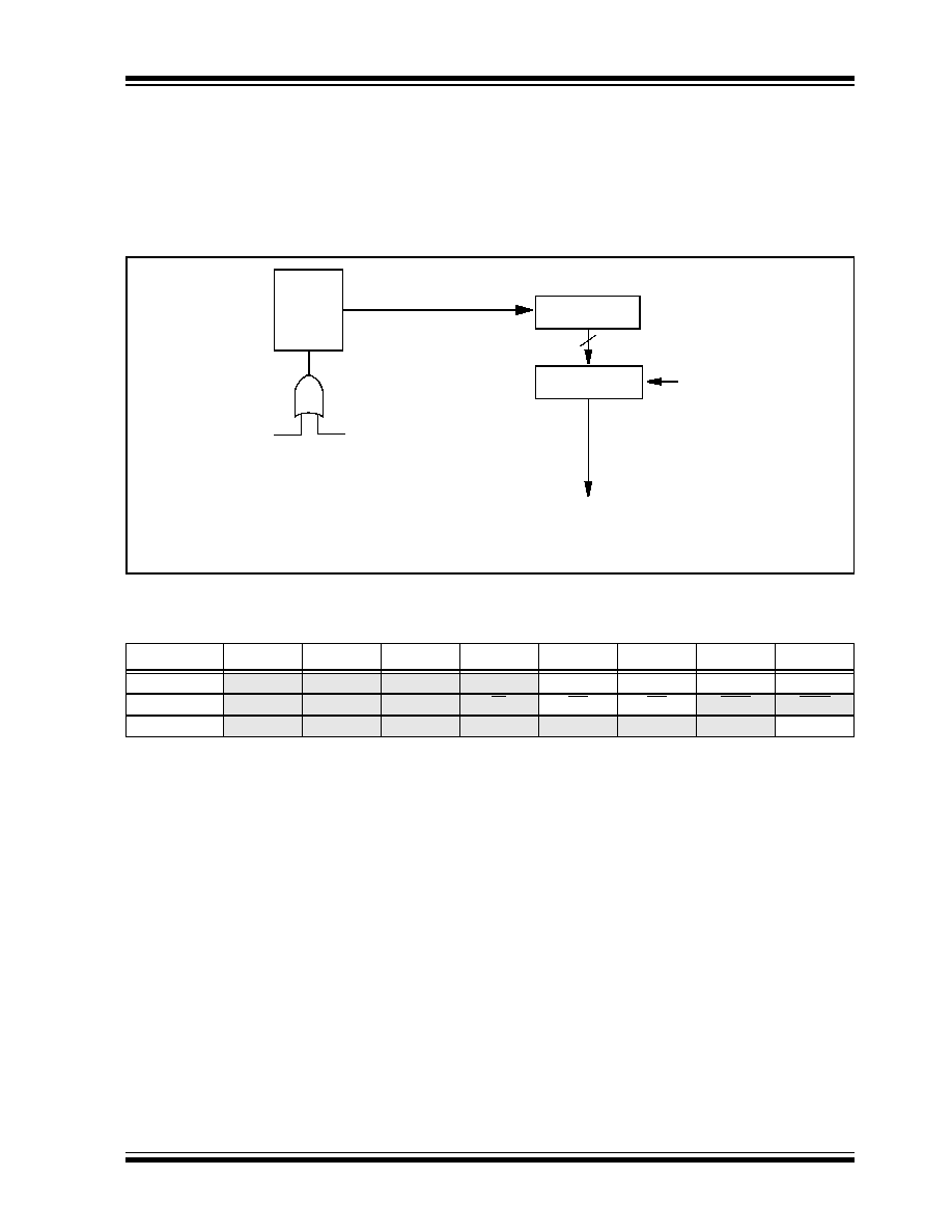
2002 Microchip Technology Inc.
Preliminary
DS41159B-page 269
PIC18FXX8
24.2.2
WDT POSTSCALER
The WDT has a postscaler that can extend the WDT
Reset period. The postscaler is selected at the time of
the device programming, by the value written to the
CONFIG2H configuration register.
FIGURE 24-1:
WATCHDOG TIMER BLOCK DIAGRAM
TABLE 24-2:
SUMMARY OF WATCHDOG TIMER REGISTERS
Postscaler
WDT Timer
WDTEN
8 - to - 1 MUX
WDTPS2:WDTPS0
WDT
Time-out
8
SWDTEN bit
Configuration bit
Note:
WDPS2:WDPS0 are bits in register CONFIG2H.
Name
Bit 7
Bit 6
Bit 5
Bit 4
Bit 3
Bit 2
Bit 1
Bit 0
CONFIG2H
--
--
--
--
WDTPS2
WDTPS2
WDTPS0
WDTEN
RCON
IPEN
--
--
RI
TO
PD
POR
BOR
WDTCON
--
--
--
--
--
--
--
SWDTEN
Legend: Shaded cells are not used by the Watchdog Timer.

PIC18FXX8
DS41159B-page 270
Preliminary
2002 Microchip Technology Inc.
24.3
Power-down Mode (SLEEP)
Power-down mode is entered by executing a
SLEEP
instruction.
If enabled, the Watchdog Timer will be cleared, but
keeps running, the PD bit (RCON<3>) is cleared, the
TO (RCON<4>) bit is set, and the oscillator driver is
turned off. The I/O ports maintain the status they had
before the
SLEEP
instruction was executed (driving
high, low or hi-impedance).
For lowest current consumption in this mode, place all
I/O pins at either V
DD
or V
SS
, ensure no external cir-
cuitry is drawing current from the I/O pin, power-down
the A/D and disable external clocks. Pull all I/O pins
that are hi-impedance inputs, high or low externally, to
avoid switching currents caused by floating inputs. The
T0CKI input should also be at V
DD
or V
SS
for lowest
current consumption. The contribution from on-chip
pull-ups on PORTB should be considered.
The MCLR pin must be at a logic high level (V
IHMC
).
24.3.1
WAKE-UP FROM SLEEP
The device can wake-up from SLEEP through one of
the following events:
1.
External RESET input on MCLR pin.
2.
Watchdog Timer Wake-up (if WDT was
enabled).
3.
Interrupt from INT pin, RB port change or a
peripheral interrupt.
The following peripheral interrupts can wake the device
from SLEEP:
1.
PSP read or write.
2.
TMR1 interrupt. Timer1 must be operating as an
asynchronous counter.
3.
TMR3 interrupt. Timer3 must be operating as an
asynchronous counter.
4.
CCP Capture mode interrupt.
5.
Special event trigger (Timer1 in Asynchronous
mode using an external clock).
6.
MSSP (START/STOP) bit detect interrupt.
7.
MSSP transmit or receive in Slave mode
(SPI/I
2
C).
8.
USART RX or TX (Synchronous Slave mode).
9.
A/D conversion (when A/D clock source is RC).
10. EEPROM write operation complete.
11. LVD interrupt.
Other peripherals cannot generate interrupts, since
during SLEEP, no on-chip clocks are present.
External MCLR Reset will cause a device RESET. All
other events are considered a continuation of program
execution and will cause a "wake-up". The TO and PD
bits in the RCON register can be used to determine the
cause of the device RESET. The PD bit, which is set on
power-up, is cleared when SLEEP is invoked. The TO
bit is cleared, if a WDT time-out occurred (and caused
wake-up).
When the
SLEEP
instruction is being executed, the next
instruction (PC + 2) is pre-fetched. For the device to
wake-up through an interrupt event, the corresponding
interrupt enable bit must be set (enabled). Wake-up is
regardless of the state of the GIE bit. If the GIE bit is
clear (disabled), the device continues execution at the
instruction after the
SLEEP
instruction. If the GIE bit is
set (enabled), the device executes the instruction after
the
SLEEP
instruction and then branches to the inter-
rupt address. In cases where the execution of the
instruction following
SLEEP
is not desirable, the user
should have a
NOP
after the
SLEEP
instruction.
24.3.2
WAKE-UP USING INTERRUPTS
When global interrupts are disabled (GIE cleared) and
any interrupt source has both its interrupt enable bit
and interrupt flag bit set, one of the following will occur:
� If an interrupt condition (interrupt flag bit and inter-
rupt enable bits are set) occurs before the execu-
tion of a
SLEEP
instruction, the
SLEEP
instruction
will complete as a
NOP
. Therefore, the WDT and
WDT postscaler will not be cleared, the TO bit will
not be set and PD bits will not be cleared.
� If the interrupt condition occurs during or after
the execution of a
SLEEP
instruction, the device
will immediately wake-up from SLEEP. The
SLEEP
instruction will be completely executed
before the wake-up. Therefore, the WDT and
WDT postscaler will be cleared, the TO bit will be
set and the PD bit will be cleared.
Even if the flag bits were checked before executing a
SLEEP
instruction, it may be possible for flag bits to
become set before the
SLEEP
instruction completes. To
determine whether a
SLEEP
instruction executed, test
the PD bit. If the PD bit is set, the
SLEEP
instruction
was executed as a
NOP
.
To ensure that the WDT is cleared, a
CLRWDT
instruction should be executed before a
SLEEP
instruction.
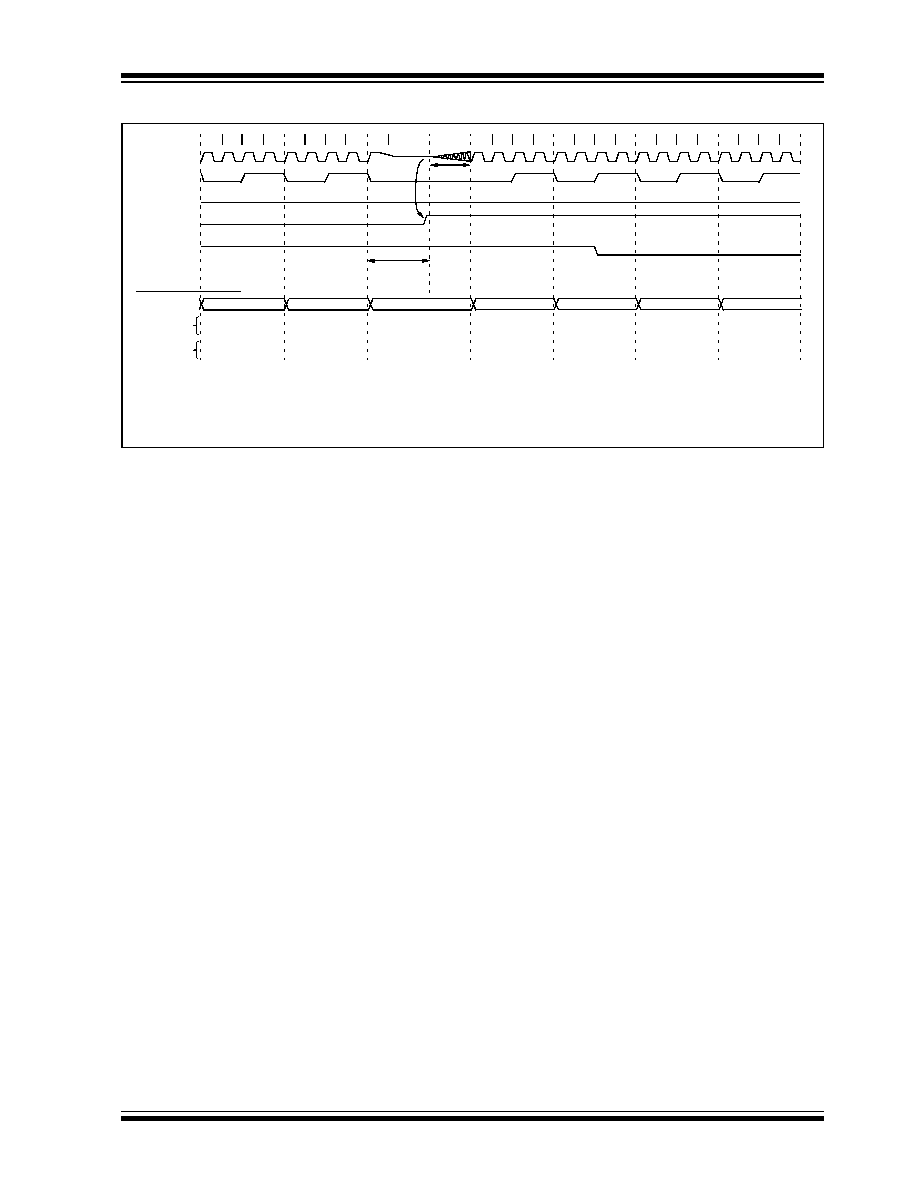
2002 Microchip Technology Inc.
Preliminary
DS41159B-page 271
PIC18FXX8
FIGURE 24-2:
WAKE-UP FROM SLEEP THROUGH INTERRUPT
(1,2)
Q1 Q2 Q3 Q4 Q1 Q2 Q3 Q4 Q1
Q1 Q2 Q3 Q4 Q1 Q2 Q3 Q4 Q1 Q2 Q3 Q4 Q1 Q2 Q3 Q4
OSC1
CLKO
(4)
INT pin
INTF flag
(INTCON<1>)
GIEH bit
(INTCON<7>)
INSTRUCTION FLOW
PC
Instruction
Fetched
Instruction
Executed
PC
PC+2
PC+4
Inst(PC) = SLEEP
Inst(PC - 1)
Inst(PC + 2)
SLEEP
Processor in
SLEEP
Interrupt Latency
(3)
Inst(PC + 4)
Inst(PC + 2)
Inst(0008h)
Inst(000Ah)
Inst(0008h)
Dummy Cycle
PC + 4
0008h
000Ah
Dummy Cycle
T
OST
(2)
PC+4
Note
1:
XT, HS or LP Oscillator mode assumed.
2:
GIE = '1' assumed. In this case, after wake-up, the processor jumps to the interrupt routine. If GIE = '0', execution will continue in-line.
3:
T
OST
= 1024 T
OSC
(drawing not to scale). This delay will not occur for RC and EC Osc modes.
4:
CLKO is not available in these Osc modes, but shown here for timing reference.

PIC18FXX8
DS41159B-page 272
Preliminary
2002 Microchip Technology Inc.
24.4
Program Verification and
Code Protection
The overall structure of the code protection on the
PIC18 FLASH devices differs significantly from other
PICmicro devices.
The user program memory is divided into five blocks.
One of these is a boot block of 512 bytes. The remain-
der of the memory is divided into four blocks on binary
boundaries.
Each of the five blocks has three code protection bits
associated with them. They are:
� Code Protect bit (CPn)
� Write Protect bit (WRTn)
� External Block Table Read bit (EBTRn)
Figure 24-3 shows the program memory organization
for 16- and 32-Kbyte devices and the specific code
protection bit associated with each block. The actual
locations of the bits are summarized in Table 24-3.
FIGURE 24-3:
CODE PROTECTED PROGRAM MEMORY FOR PIC18F2X8/4X8
TABLE 24-3:
SUMMARY OF CODE PROTECTION REGISTERS
MEMORY SIZE/DEVICE
Block Code Protection
Controlled By:
16 Kbytes
(PIC18FX48)
32 Kbytes
(PIC18FX58)
Address
Range
Boot Block
Boot Block
000000h
0001FFh
CPB, WRTB, EBTRB
Block 0
Block 0
000200h
001FFFh
CP0, WRT0, EBTR0
Block 1
Block 1
002000h
003FFFh
CP1, WRT1, EBTR1
Unimplemented
Read 0s
Block 2
004000h
005FFFh
CP2, WRT2, EBTR2
Unimplemented
Read 0s
Block 3
006000h
007FFFh
CP3, WRT3, EBTR3
Unimplemented
Read 0s
Unimplemented
Read 0s
008000h
1FFFFFh
(Unimplemented Memory Space)
File Name
Bit 7
Bit 6
Bit 5
Bit 4
Bit 3
Bit 2
Bit 1
Bit 0
300008h
CONFIG5L
--
--
--
--
CP3
CP2
CP1
CP0
300009h
CONFIG5H
CPD
CPB
--
--
--
--
--
--
30000Ah
CONFIG6L
--
--
--
--
WRT3
WRT2
WRT1
WRT0
30000Bh
CONFIG6H
WRTD
WRTB
WRTC
--
--
--
--
--
30000Ch
CONFIG7L
--
--
--
--
EBTR3
EBTR2
EBTR1
EBTR0
30000Dh
CONFIG7H
--
EBTRB
--
--
--
--
--
--
Legend: Shaded cells are unimplemented.
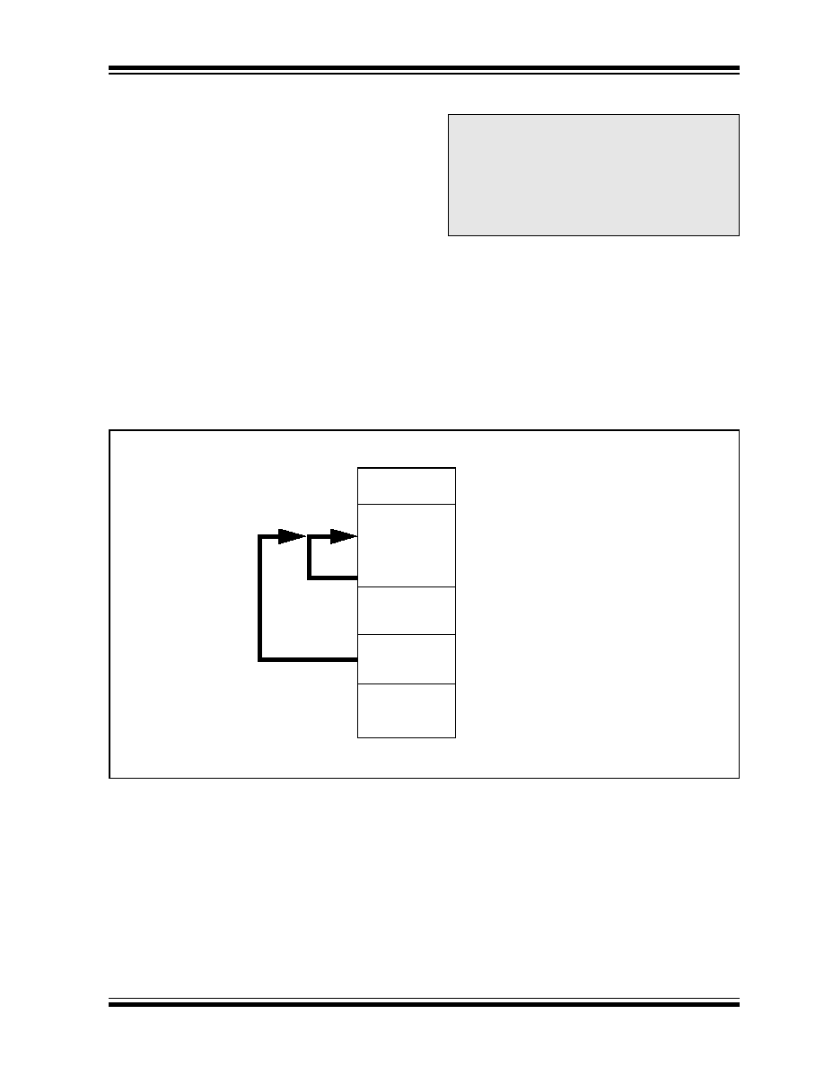
2002 Microchip Technology Inc.
Preliminary
DS41159B-page 273
PIC18FXX8
24.4.1
PROGRAM MEMORY
CODE PROTECTION
The user memory may be read to or written from any
location using the Table Read and Table Write instruc-
tions. The device ID may be read with Table Reads.
The configuration registers may be read and written
with the Table Read and Table Write instructions.
In User mode, the CPn bits have no direct effect. CPn
bits inhibit external reads and writes. A block of user
memory may be protected from Table Writes if the
WRTn configuration bit is `
0
'. The EBTRn bits control
Table Reads. For a block of user memory with the
EBTRn bit set to `
0',
a Table Read instruction that
executes from within that block is allowed to read. A
Table Read instruction that executes from a location
outside of that block is not allowed to read, and will
result in reading `0's. Figures 24-4 through 24-6
illustrate Table Write and Table Read protection.
FIGURE 24-4:
TABLE WRITE (WRTn) DISALLOWED
Note:
Code protection bits may only be written to
a `0' from a `1' state. It is not possible to
write a `1' to a bit in the `0' state. Code pro-
tection bits are only set to `1' by a full chip
erase or block erase function. The full chip
erase and block erase functions can only
be initiated via ICSP or an external
programmer.
000000h
0001FFh
000200h
001FFFh
002000h
003FFFh
004000h
005FFFh
006000h
007FFFh
WRTB,EBTRB =
11
WRT0,EBTR0 =
01
WRT1,EBTR1 =
11
WRT2,EBTR2 =
11
WRT3,EBTR3 =
11
TBLWT *
TBLPTR = 000FFF
PC = 001FFE
TBLWT *
PC = 004FFE
Register Values
Program Memory
Configuration Bit Settings
Results: All Table Writes disabled to Blockn whenever WRTn = `0'
.
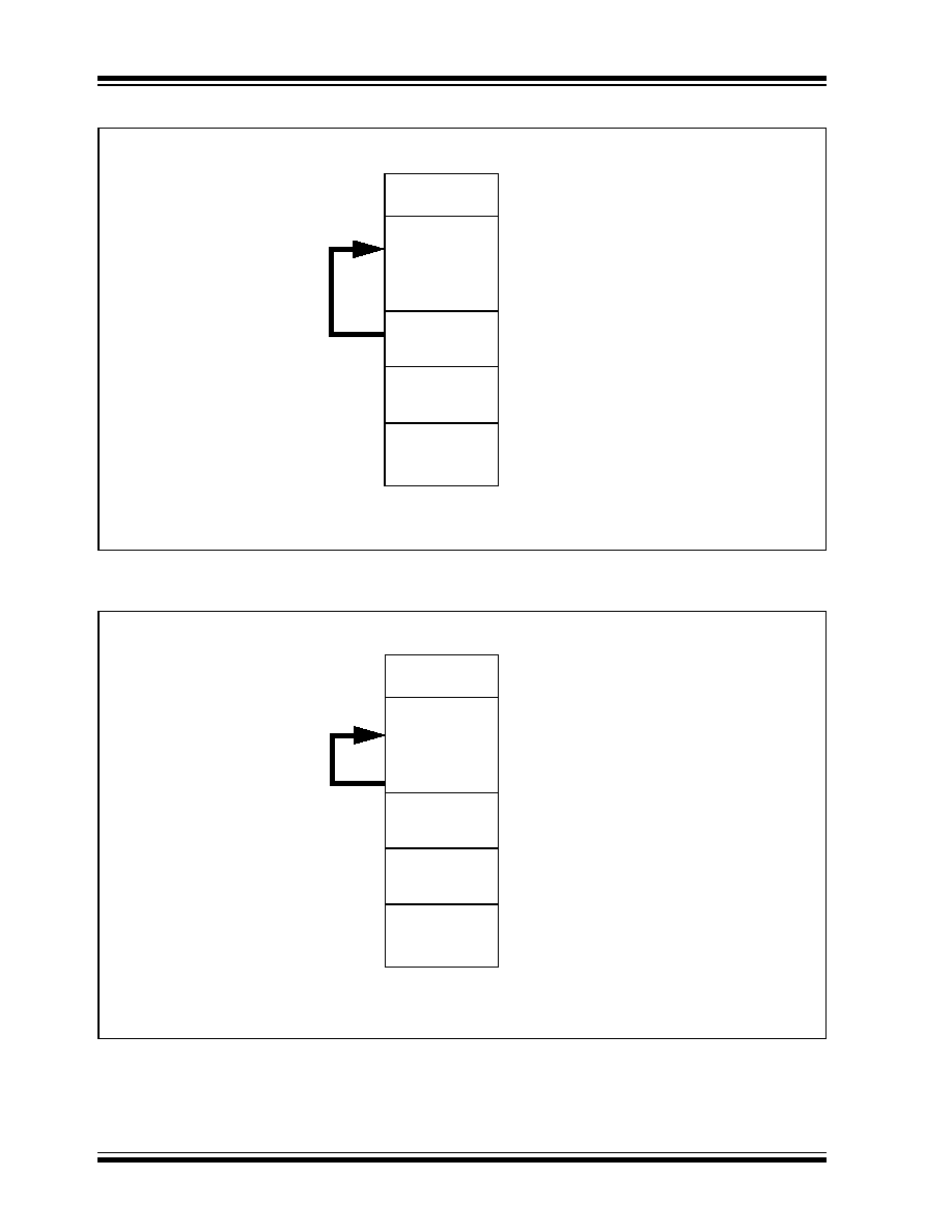
PIC18FXX8
DS41159B-page 274
Preliminary
2002 Microchip Technology Inc.
FIGURE 24-5:
EXTERNAL BLOCK TABLE READ (EBTRn) DISALLOWED
FIGURE 24-6:
EXTERNAL BLOCK TABLE READ (EBTRn) ALLOWED
000000h
0001FFh
000200h
001FFFh
002000h
003FFFh
004000h
005FFFh
006000h
007FFFh
WRTB,EBTRB =
11
WRT0,EBTR0 =
10
WRT1,EBTR1 =
11
WRT2,EBTR2 =
11
WRT3,EBTR3 =
11
TBLRD *
TBLPTR = 000FFF
PC = 002FFE
Results: All Table Reads from external blocks to Blockn are disabled whenever EBTRn = `0'.
TABLAT register returns a value of "0".
Register Values
Program Memory
Configuration Bit Settings
000000h
0001FFh
000200h
001FFFh
002000h
003FFFh
004000h
005FFFh
006000h
007FFFh
WRTB,EBTRB =
11
WRT0,EBTR0 =
10
WRT1,EBTR1 =
11
WRT2,EBTR2 =
11
WRT3,EBTR3 =
11
TBLRD *
TBLPTR = 000FFF
PC = 001FFE
Register Values
Program Memory
Configuration Bit Settings
Results: Table Reads permitted within Blockn, even when EBTRBn = `0'.
TABLAT register returns the value of the data at the location TBLPTR.

2002 Microchip Technology Inc.
Preliminary
DS41159B-page 275
PIC18FXX8
24.4.2
DATA EEPROM
CODE PROTECTION
The entire data EEPROM is protected from external
reads and writes by two bits: CPD and WRTD. CPD
inhibits external reads and writes of data EEPROM.
WRTD inhibits external writes to data EEPROM. The
CPU can continue to read and write data EEPROM,
regardless of the protection bit settings.
24.4.3
CONFIGURATION REGISTER
PROTECTION
The configuration registers can be write protected. The
WRTC bit controls protection of the configuration regis-
ters. In User mode, the WRTC bit is readable only.
WRTC can only be written via ICSP or an external
programmer.
24.5
ID Locations
Eight memory locations (200000h - 200007h) are des-
ignated as ID locations, where the user can store
checksum or other code identification numbers. These
locations are accessible during normal execution
through the
TBLRD
and
TBLWT
instructions, or during
program/verify. The ID locations can be read when the
device is code protected.
24.6
In-Circuit Serial Programming
PIC18FXXX microcontrollers can be serially pro-
grammed while in the end application circuit. This is
simply done with two lines for clock and data, and three
other lines for power, ground and the programming
voltage. This allows customers to manufacture boards
with unprogrammed devices, and then program the
microcontroller just before shipping the product. This
also allows the most recent firmware or a custom
firmware to be programmed.
24.7
In-Circuit Debugger
When the DEBUG bit in configuration register
CONFIG4L is programmed to a '
0
', the In-Circuit
Debugger functionality is enabled. This function allows
simple debugging functions when used with MPLAB
�
IDE. When the microcontroller has this feature
enabled, some of the resources are not available for
general use. Resources used include 2 I/O pins, stack
locations, program memory and data memory. For
more information on the resources required, see the
User's Guide for the In-Circuit Debugger you are using.
To use the In-Circuit Debugger function of the micro-
controller, the design must implement In-Circuit Serial
Programming connections to MCLR/V
PP
, V
DD
, GND,
RB7 and RB6. This will interface to the In-Circuit
Debugger module available from Microchip, or one of
the third party development tool companies. The
Microchip In-Circuit Debugger (ICD) used with the
PIC18FXXX microcontrollers is the MPLAB
�
ICD 2.
24.8
Low Voltage ICSP Programming
The LVP bit configuration register CONFIG4L enables
low voltage ICSP programming. This mode allows the
microcontroller to be programmed via ICSP using a
V
DD
source in the operating voltage range. This only
means that V
PP
does not have to be brought to V
IHH
,
but can instead be left at the normal operating voltage.
In this mode, the RB5/PGM pin is dedicated to the pro-
gramming function and ceases to be a general purpose
I/O pin. During programming, V
DD
is applied to the
MCLR/V
PP
pin. To enter Programming mode, V
DD
must
be applied to the RB5/PGM, provided the LVP bit is set.
The LVP bit defaults to a (`1') from the factory.
If Low Voltage Programming mode is not used, the LVP
bit can be programmed to a '0' and RB5/PGM becomes
a digital I/O pin. However, the LVP bit may only be pro-
grammed when programming is entered with V
IHH
on
MCLR/V
PP
. The LVP bit can only be charged when
using high voltage on MCLR.
It should be noted that once the LVP bit is programmed
to 0, only the High Voltage Programming mode is avail-
able and only High Voltage Programming mode can be
used to program the device.
When using Low Voltage ICSP, the part must be sup-
plied 4.5V to 5.5V, if a bulk erase will be executed. This
includes reprogramming of the code protect bits from
an on-state to off-state. For all other cases of Low Volt-
age ICSP, the part may be programmed at the normal
operating voltage. This means unique user IDs, or user
code can be reprogrammed or added.
Note 1: The High Voltage Programming mode is
always available, regardless of the state
of the LVP bit, by applying V
IHH
to the
MCLR pin.
2: While in Low Voltage ICSP mode, the
RB5 pin can no longer be used as a
general purpose I/O pin.
3: When using Low Voltage ICSP program-
ming (LVP) and the pull-ups on PORTB
are enabled, bit 5 in the TRISB register
must be cleared to disable the pull-up on
RB5 and ensure the proper operation of
the device.

PIC18FXX8
DS41159B-page 276
Preliminary
2002 Microchip Technology Inc.
NOTES:

2002 Microchip Technology Inc.
DS41159B-page 277
PIC18FXX8
25.0
INSTRUCTION SET SUMMARY
The PIC18 instruction set adds many enhancements to
the previous PICmicro instruction sets, while maintaining
an easy migration from these PICmicro instruction sets.
Most instructions are a single program memory word
(16 bits), but there are three instructions that require
two program memory locations.
Each single word instruction is a 16-bit word divided
into an OPCODE, which specifies the instruction type
and one or more operands, which further specify the
operation of the instruction.
The instruction set is highly orthogonal and is grouped
into four basic categories:
� Byte-oriented operations
� Bit-oriented operations
� Literal operations
� Control operations
The PIC18 instruction set summary in Table 25-2 lists
byte-oriented, bit-oriented, literal and control
operations. Table 25-1 shows the opcode field
descriptions.
Most byte-oriented instructions have three operands:
1.
The file register (specified by `f')
2.
The destination of the result
(specified by `d')
3.
The accessed memory
(specified by `a')
The file register designator 'f' specifies which file
register is to be used by the instruction.
The destination designator `d' specifies where the
result of the operation is to be placed. If 'd' is zero, the
result is placed in the WREG register. If 'd' is one, the
result is placed in the file register specified in the
instruction.
All bit-oriented instructions have three operands:
1.
The file register (specified by `f')
2.
The bit in the file register
(specified by `b')
3.
The accessed memory
(specified by `a')
The bit field designator 'b' selects the number of the bit
affected by the operation, while the file register desig-
nator 'f' represents the number of the file in which the
bit is located.
The literal instructions may use some of the following
operands:
� A literal value to be loaded into a file register
(specified by `k')
� The desired FSR register to load the literal value
into (specified by `f')
� No operand required
(specified by `--')
The control instructions may use some of the following
operands:
� A program memory address (specified by `n')
� The mode of the Call or Return instructions
(specified by `s')
� The mode of the Table Read and Table Write
instructions (specified by `m')
� No operand required
(specified by `--')
All instructions are a single word, except for three
double-word instructions. These three instructions
were made double-word instructions so that all the
required information is available in these 32 bits. In the
second word, the 4 MSbs are 1's. If this second word is
executed as an instruction (by itself), it will execute as
a
NOP
.
All single word instructions are executed in a single
instruction cycle, unless a conditional test is true or the
program counter is changed as a result of the instruc-
tion. In these cases, the execution takes two instruction
cycles, with the additional instruction cycle(s) executed
as a
NOP
.
The double-word instructions execute in two instruction
cycles.
One instruction cycle consists of four oscillator periods.
Thus, for an oscillator frequency of 4 MHz, the normal
instruction execution time is 1
�
s. If a conditional test is
true, or the program counter is changed as a result of
an instruction, the instruction execution time is 2
�
s.
Two-word branch instructions (if true) would take 3
�
s.
Figure 25-1 shows the general formats that the
instructions can have.
All examples use the format
`nnh'
to represent a
hexadecimal number, where
`h'
signifies a
hexadecimal digit.
The Instruction Set Summary, shown in Table 25-2,
lists the instructions recognized by the Microchip
Assembler (MPASM
TM
).
Section 25.2 provides a description of each instruction.
25.1
READ-MODIFY-WRITE
OPERATIONS
Any instruction that specifies a file register as part of
the instruction performs a Read-Modify-Write (R-M-W)
operation. The register is read, the data is modified,
and the result is stored according to either the instruc-
tion or the destination designator `d'. A read operation
is performed on a register even if the instruction writes
to that register.
For example, a "
clrf PORTB
" instruction will read
PORTB, clear all the data bits, then write the result
back to PORTB. This example would have the unin-
tended result that the condition that sets the RBIF flag
would be cleared.

PIC18FXX8
DS41159B-page 278
2002 Microchip Technology Inc.
TABLE 25-1:
OPCODE FIELD DESCRIPTIONS
Field
Description
a
RAM access bit
a = 0: RAM location in Access RAM (BSR register is ignored)
a = 1: RAM bank is specified by BSR register
bbb
Bit address within an 8-bit file register (0 to 7)
BSR
Bank Select Register. Used to select the current RAM bank.
d
Destination select bit;
d = 0: store result in WREG,
d = 1: store result in file register f.
dest
Destination either the WREG register or the specified register file location
f
8-bit Register file address (0x00 to 0xFF)
fs
12-bit Register file address (0x000 to 0xFFF). This is the source address.
fd
12-bit Register file address (0x000 to 0xFFF). This is the destination address.
k
Literal field, constant data or label (may be either an 8-bit, 12-bit or a 20-bit value)
label
Label name
mm
The mode of the TBLPTR register for the Table Read and Table Write instructions.
Only used with Table Read and Table Write instructions:
*
No change to register (such as TBLPTR with Table Reads and Writes)
*+
Post-Increment register (such as TBLPTR with Table Reads and Writes)
*-
Post-Decrement register (such as TBLPTR with Table Reads and Writes)
+*
Pre-Increment register (such as TBLPTR with Table Reads and Writes)
n
The relative address (2's complement number) for relative branch instructions, or the direct address for
Call/Branch and Return instructions
PRODH
Product of Multiply high byte
PRODL
Product of Multiply low byte
s
Fast Call/Return mode select bit;
s = 0: do not update into/from shadow registers
s = 1: certain registers loaded into/from shadow registers (Fast mode)
u
Unused or Unchanged
WREG
Working register (accumulator)
x
Don't care (0 or 1).
The assembler will generate code with x = 0. It is the recommended form of use for compatibility with all
Microchip software tools.
TBLPTR
21-bit Table Pointer (points to a Program Memory location)
TABLAT
8-bit Table Latch
TOS
Top-of-Stack
PC
Program Counter
PCL
Program Counter Low Byte
PCH
Program Counter High Byte
PCLATH
Program Counter High Byte Latch
PCLATU
Program Counter Upper Byte Latch
GIE
Global Interrupt Enable bit
WDT
Watchdog Timer
TO
Time-out bit
PD
Power-down bit
C, DC, Z, OV, N
ALU status bits Carry, Digit Carry, Zero, Overflow, Negative
[ ]
Optional
( )
Contents
Assigned to
< >
Register bit field
In the set of
italics
User defined term (font is courier)
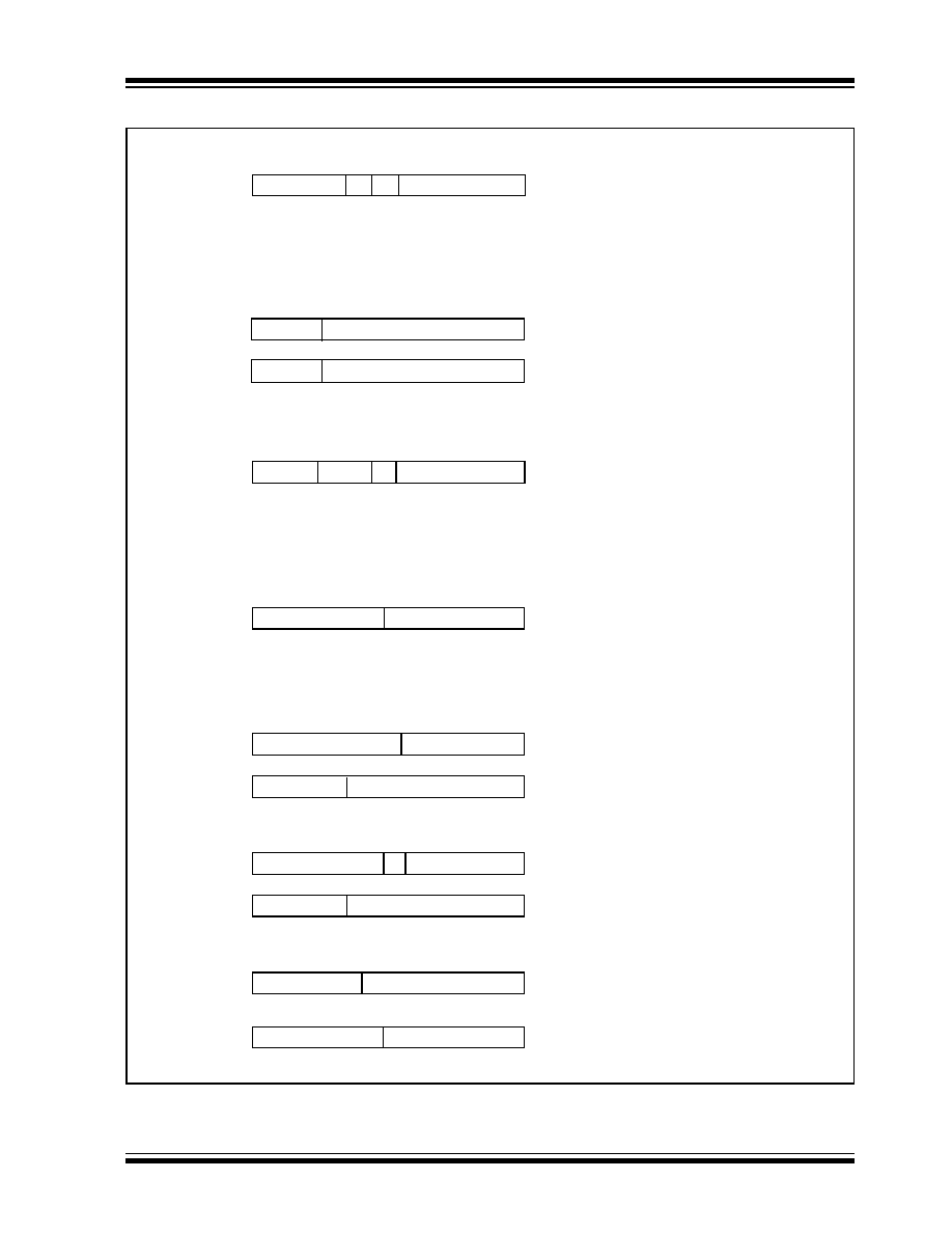
2002 Microchip Technology Inc.
DS41159B-page 279
PIC18FXX8
FIGURE 25-1:
GENERAL FORMAT FOR INSTRUCTIONS
Byte-oriented file register operations
15 10 9 8 7 0
d = 0 for result destination to be WREG register
OPCODE d a f (FILE #)
d = 1 for result destination to be file register (f)
a = 0 to force Access Bank
Bit-oriented file register operations
15 12 11 9 8 7 0
OPCODE b (BIT #) a f (FILE #)
b = 3-bit position of bit in file register (f)
Literal operations
15 8 7 0
OPCODE k (literal)
k = 8-bit immediate value
Byte to Byte move operations (2-word)
15 12 11 0
OPCODE f (Source FILE #)
CALL, GOTO and Branch operations
15 8 7 0
OPCODE n<7:0> (literal)
n = 20-bit immediate value
a = 1 for BSR to select bank
f = 8-bit file register address
a = 0 to force Access Bank
a = 1 for BSR to select bank
f = 8-bit file register address
15 12 11 0
1111
n<19:8> (literal)
15 12 11 0
1111
f (Destination FILE #)
f = 12-bit file register address
Control operations
Example Instruction
ADDWF MYREG, W, B
MOVFF MYREG1, MYREG2
BSF MYREG, bit, B
MOVLW 0x7F
GOTO Label
15 8 7 0
OPCODE n<7:0> (literal)
15 12 11 0
n<19:8> (literal)
CALL MYFUNC
15 11 10 0
OPCODE n<10:0> (literal)
S = Fast bit
BRA MYFUNC
15 8 7 0
OPCODE n<7:0> (literal)
BC MYFUNC
S

PIC18FXX8
DS41159B-page 280
2002 Microchip Technology Inc.
TABLE 25-2:
PIC18FXXX INSTRUCTION SET
Mnemonic,
Operands
Description
Cycles
16-Bit Instruction Word
Status
Affected
Notes
MSb
LSb
BYTE-ORIENTED FILE REGISTER OPERATIONS
ADDWF
ADDWFC
ANDWF
CLRF
COMF
CPFSEQ
CPFSGT
CPFSLT
DECF
DECFSZ
DCFSNZ
INCF
INCFSZ
INFSNZ
IORWF
MOVF
MOVFF
MOVWF
MULWF
NEGF
RLCF
RLNCF
RRCF
RRNCF
SETF
SUBFWB
SUBWF
SUBWFB
SWAPF
TSTFSZ
XORWF
f, d, a
f, d, a
f, d, a
f, a
f, d, a
f, a
f, a
f, a
f, d, a
f, d, a
f, d, a
f, d, a
f, d, a
f, d, a
f, d, a
f, d, a
f
s
, f
d
f, a
f, a
f, a
f, d, a
f, d, a
f, d, a
f, d, a
f, a
f, d, a
f, d, a
f, d, a
f, d, a
f, a
f, d, a
Add WREG and f
Add WREG and Carry bit to f
AND WREG with f
Clear f
Complement f
Compare f with WREG, skip =
Compare f with WREG, skip >
Compare f with WREG, skip <
Decrement f
Decrement f, Skip if 0
Decrement f, Skip if Not 0
Increment f
Increment f, Skip if 0
Increment f, Skip if Not 0
Inclusive OR WREG with f
Move f
Move f
s
(source) to 1st word
f
d
(destination) 2nd word
Move WREG to f
Multiply WREG with f
Negate f
Rotate Left f through Carry
Rotate Left f (No Carry)
Rotate Right f through Carry
Rotate Right f (No Carry)
Set f
Subtract f from WREG with
borrow
Subtract WREG from f
Subtract WREG from f with
borrow
Swap nibbles in f
Test f, skip if 0
Exclusive OR WREG with f
1
1
1
1
1
1 (2 or 3)
1 (2 or 3)
1 (2 or 3)
1
1 (2 or 3)
1 (2 or 3)
1
1 (2 or 3)
1 (2 or 3)
1
1
2
1
1
1
1
1
1
1
1
1
1
1
1
1 (2 or 3)
1
0010
0010
0001
0110
0001
0110
0110
0110
0000
0010
0100
0010
0011
0100
0001
0101
1100
1111
0110
0000
0110
0011
0100
0011
0100
0110
0101
0101
0101
0011
0110
0001
01da
00da
01da
101a
11da
001a
010a
000a
01da
11da
11da
10da
11da
10da
00da
00da
ffff
ffff
111a
001a
110a
01da
01da
00da
00da
100a
01da
11da
10da
10da
011a
10da
ffff
ffff
ffff
ffff
ffff
ffff
ffff
ffff
ffff
ffff
ffff
ffff
ffff
ffff
ffff
ffff
ffff
ffff
ffff
ffff
ffff
ffff
ffff
ffff
ffff
ffff
ffff
ffff
ffff
ffff
ffff
ffff
ffff
ffff
ffff
ffff
ffff
ffff
ffff
ffff
ffff
ffff
ffff
ffff
ffff
ffff
ffff
ffff
ffff
ffff
ffff
ffff
ffff
ffff
ffff
ffff
ffff
ffff
ffff
ffff
ffff
ffff
ffff
ffff
C, DC, Z, OV, N
C, DC, Z, OV, N
Z, N
Z
Z, N
None
None
None
C, DC, Z, OV, N
None
None
C, DC, Z, OV, N
None
None
Z, N
Z, N
None
None
None
C, DC, Z, OV, N
C, Z, N
Z, N
C, Z, N
Z, N
None
C, DC, Z, OV, N
C, DC, Z, OV, N
C, DC, Z, OV, N
None
None
Z, N
1, 2
1, 2
1,2
2
1, 2
4
4
1, 2
1, 2, 3, 4
1, 2, 3, 4
1, 2
1, 2, 3, 4
4
1, 2
1, 2
1
1, 2
1, 2
1, 2
1, 2
4
1, 2
BIT-ORIENTED FILE REGISTER OPERATIONS
BCF
BSF
BTFSC
BTFSS
BTG
f, b, a
f, b, a
f, b, a
f, b, a
f, d, a
Bit Clear f
Bit Set f
Bit Test f, Skip if Clear
Bit Test f, Skip if Set
Bit Toggle f
1
1
1 (2 or 3)
1 (2 or 3)
1
1001
1000
1011
1010
0111
bbba
bbba
bbba
bbba
bbba
ffff
ffff
ffff
ffff
ffff
ffff
ffff
ffff
ffff
ffff
None
None
None
None
None
1, 2
1, 2
3, 4
3, 4
1, 2
Note 1: When a PORT register is modified as a function of itself (e.g.,
MOVF PORTB, 1, 0
), the value used will be
that value present on the pins themselves. For example, if the data latch is '1' for a pin configured as input and
is driven low by an external device, the data will be written back with a '0'.
2: If this instruction is executed on the TMR0 register (and, where applicable, d = 1), the prescaler will be
cleared if assigned.
3: If Program Counter (PC) is modified or a conditional test is true, the instruction requires two cycles. The
second cycle is executed as a
NOP
.
4: Some instructions are 2-word instructions. The second word of these instructions will be executed as a
NOP
,
unless the first word of the instruction retrieves the information embedded in these 16 bits. This ensures that
all program memory locations have a valid instruction.
5: If the Table Write starts the write cycle to internal memory, the write will continue until terminated.

2002 Microchip Technology Inc.
DS41159B-page 281
PIC18FXX8
CONTROL OPERATIONS
BC
BN
BNC
BNN
BNOV
BNZ
BOV
BRA
BZ
CALL
CLRWDT
DAW
GOTO
NOP
NOP
POP
PUSH
RCALL
RESET
RETFIE
RETLW
RETURN
SLEEP
n
n
n
n
n
n
n
n
n
n, s
--
--
n
--
--
--
--
n
s
k
s
--
Branch if Carry
Branch if Negative
Branch if Not Carry
Branch if Not Negative
Branch if Not Overflow
Branch if Not Zero
Branch if Overflow
Branch Unconditionally
Branch if Zero
Call subroutine 1st word
2nd word
Clear Watchdog Timer
Decimal Adjust WREG
Go to address 1st word
2nd word
No Operation
No Operation (Note 4)
Pop top of return stack (TOS)
Push top of return stack (TOS)
Relative Call
Software device RESET
Return from interrupt enable
Return with literal in WREG
Return from Subroutine
Go into Standby mode
1 (2)
1 (2)
1 (2)
1 (2)
1 (2)
2
1 (2)
1 (2)
1 (2)
2
1
1
2
1
1
1
1
2
1
2
2
2
1
1110
1110
1110
1110
1110
1110
1110
1101
1110
1110
1111
0000
0000
1110
1111
0000
1111
0000
0000
1101
0000
0000
0000
0000
0000
0010
0110
0011
0111
0101
0001
0100
0nnn
0000
110s
kkkk
0000
0000
1111
kkkk
0000
xxxx
0000
0000
1nnn
0000
0000
1100
0000
0000
nnnn
nnnn
nnnn
nnnn
nnnn
nnnn
nnnn
nnnn
nnnn
kkkk
kkkk
0000
0000
kkkk
kkkk
0000
xxxx
0000
0000
nnnn
1111
0001
kkkk
0001
0000
nnnn
nnnn
nnnn
nnnn
nnnn
nnnn
nnnn
nnnn
nnnn
kkkk
kkkk
0100
0111
kkkk
kkkk
0000
xxxx
0110
0101
nnnn
1111
000s
kkkk
001s
0011
None
None
None
None
None
None
None
None
None
None
TO
,
PD
C
None
None
None
None
None
None
All
GIE/GIEH,
PEIE/GIEL
None
None
TO
,
PD
TABLE 25-2:
PIC18FXXX INSTRUCTION SET (CONTINUED)
Mnemonic,
Operands
Description
Cycles
16-Bit Instruction Word
Status
Affected
Notes
MSb
LSb
Note 1: When a PORT register is modified as a function of itself (e.g.,
MOVF PORTB, 1, 0
), the value used will be
that value present on the pins themselves. For example, if the data latch is '1' for a pin configured as input and
is driven low by an external device, the data will be written back with a '0'.
2: If this instruction is executed on the TMR0 register (and, where applicable, d = 1), the prescaler will be
cleared if assigned.
3: If Program Counter (PC) is modified or a conditional test is true, the instruction requires two cycles. The
second cycle is executed as a
NOP
.
4: Some instructions are 2-word instructions. The second word of these instructions will be executed as a
NOP
,
unless the first word of the instruction retrieves the information embedded in these 16 bits. This ensures that
all program memory locations have a valid instruction.
5: If the Table Write starts the write cycle to internal memory, the write will continue until terminated.

PIC18FXX8
DS41159B-page 282
2002 Microchip Technology Inc.
LITERAL OPERATIONS
ADDLW
ANDLW
IORLW
LFSR
MOVLB
MOVLW
MULLW
RETLW
SUBLW
XORLW
k
k
k
f, k
k
k
k
k
k
k
Add literal and WREG
AND literal with WREG
Inclusive OR literal with WREG
Move literal (12-bit) 2nd word
to FSRx 1st word
Move literal to BSR<3:0>
Move literal to WREG
Multiply literal with WREG
Return with literal in WREG
Subtract WREG from literal
Exclusive OR literal with WREG
1
1
1
2
1
1
1
2
1
1
0000
0000
0000
1110
1111
0000
0000
0000
0000
0000
0000
1111
1011
1001
1110
0000
0001
1110
1101
1100
1000
1010
kkkk
kkkk
kkkk
00ff
kkkk
0000
kkkk
kkkk
kkkk
kkkk
kkkk
kkkk
kkkk
kkkk
kkkk
kkkk
kkkk
kkkk
kkkk
kkkk
kkkk
kkkk
C, DC, Z, OV, N
Z, N
Z, N
None
None
None
None
None
C, DC, Z, OV, N
Z, N
DATA MEMORY
PROGRAM MEMORY OPERATIONS
TBLRD*
TBLRD*+
TBLRD*-
TBLRD+*
TBLWT*
TBLWT*+
TBLWT*-
TBLWT+*
Table Read
Table Read with post-increment
Table Read with post-decrement
Table Read with pre-increment
Table Write
Table Write with post-increment
Table Write with post-decrement
Table Write with pre-increment
2
2 (5)
0000
0000
0000
0000
0000
0000
0000
0000
0000
0000
0000
0000
0000
0000
0000
0000
0000
0000
0000
0000
0000
0000
0000
0000
1000
1001
1010
1011
1100
1101
1110
1111
None
None
None
None
None
None
None
None
TABLE 25-2:
PIC18FXXX INSTRUCTION SET (CONTINUED)
Mnemonic,
Operands
Description
Cycles
16-Bit Instruction Word
Status
Affected
Notes
MSb
LSb
Note 1: When a PORT register is modified as a function of itself (e.g.,
MOVF PORTB, 1, 0
), the value used will be
that value present on the pins themselves. For example, if the data latch is '1' for a pin configured as input and
is driven low by an external device, the data will be written back with a '0'.
2: If this instruction is executed on the TMR0 register (and, where applicable, d = 1), the prescaler will be
cleared if assigned.
3: If Program Counter (PC) is modified or a conditional test is true, the instruction requires two cycles. The
second cycle is executed as a
NOP
.
4: Some instructions are 2-word instructions. The second word of these instructions will be executed as a
NOP
,
unless the first word of the instruction retrieves the information embedded in these 16 bits. This ensures that
all program memory locations have a valid instruction.
5: If the Table Write starts the write cycle to internal memory, the write will continue until terminated.
2002 Microchip Technology Inc.
DS41159B-page 283
PIC18FXX8
25.2
Instruction Set
ADDLW
ADD literal to W
Syntax:
[ label ] ADDLW k
Operands:
0
k
255
Operation:
(W) + k
W
Status Affected:
N, OV, C, DC, Z
Encoding:
0000
1111
kkkk
kkkk
Description:
The contents of W are added to the
8-bit literal 'k' and the result is
placed in W.
Words:
1
Cycles:
1
Q Cycle Activity:
Q1
Q2
Q3
Q4
Decode
Read
literal 'k'
Process
Data
Write to W
Example:
ADDLW
0x15
Before Instruction
W
=
0x10
After Instruction
W = 0x25
ADDWF
ADD W to f
Syntax:
[ label ] ADDWF f [,d [,a]]
Operands:
0
f
255
d
[0,1]
a
[0,1]
Operation:
(W) + (f)
dest
Status Affected:
N, OV, C, DC, Z
Encoding:
0010
01da
ffff
ffff
Description:
Add W to register 'f'. If 'd' is 0, the
result is stored in W. If 'd' is 1, the
result is stored back in register 'f'
(default). If `a' is 0, the Access
Bank will be selected. If `a' is 1, the
BSR is used.
Words:
1
Cycles:
1
Q Cycle Activity:
Q1
Q2
Q3
Q4
Decode
Read
register 'f'
Process
Data
Write to
destination
Example:
ADDWF
REG,
W
Before Instruction
W
=
0x17
REG
=
0xC2
After Instruction
W
=
0xD9
REG
=
0xC2

PIC18FXX8
DS41159B-page 284
2002 Microchip Technology Inc.
ADDWFC
ADD W and Carry bit to f
Syntax:
[ label ] ADDWFC f [,d [,a]]
Operands:
0
f
255
d
[0,1]
a
[0,1]
Operation:
(W) + (f) + (C)
dest
Status Affected:
N, OV, C, DC, Z
Encoding:
0010
00da
ffff
ffff
Description:
Add W, the Carry Flag and data
memory location 'f'. If 'd' is 0, the
result is placed in W. If 'd' is 1, the
result is placed in data memory loca-
tion 'f'. If `a' is 0, the Access Bank
will be selected. If `a' is 1, the BSR
will not be overridden.
Words:
1
Cycles:
1
Q Cycle Activity:
Q1
Q2
Q3
Q4
Decode
Read
register 'f'
Process
Data
Write to
destination
Example:
ADDWFC
REG,
W
Before Instruction
Carry bit =
1
REG
=
0x02
W
=
0x4D
After Instruction
Carry bit =
0
REG
=
0x02
W
=
0x50
ANDLW
AND literal with W
Syntax:
[ label ] ANDLW k
Operands:
0
k
255
Operation:
(W) .AND. k
W
Status Affected:
N, Z
Encoding:
0000
1011
kkkk
kkkk
Description:
The contents of W are ANDed with
the 8-bit literal 'k'. The result is
placed in W.
Words:
1
Cycles:
1
Q Cycle Activity:
Q1
Q2
Q3
Q4
Decode
Read literal
'k'
Process
Data
Write to W
Example:
ANDLW
0x5F
Before Instruction
W
=
0xA3
After Instruction
W
=
0x03

2002 Microchip Technology Inc.
DS41159B-page 285
PIC18FXX8
ANDWF
AND W with f
Syntax:
[ label ] ANDWF f [,d [,a]]
Operands:
0
f
255
d
[0,1]
a
[0,1]
Operation:
(W) .AND. (f)
dest
Status Affected:
N, Z
Encoding:
0001
01da
ffff
ffff
Description:
The contents of W are AND'ed with
register 'f'. If 'd' is 0, the result is
stored in W. If 'd' is 1, the result is
stored back in register 'f' (default). If
`a' is 0, the Access Bank will be
selected. If `a' is 1, the BSR will not
be overridden (default).
Words:
1
Cycles:
1
Q Cycle Activity:
Q1
Q2
Q3
Q4
Decode
Read
register 'f'
Process
Data
Write to
destination
Example:
ANDWF
REG,
W
Before Instruction
W
=
0x17
REG
=
0xC2
After Instruction
W
=
0x02
REG
=
0xC2
BC
Branch if Carry
Syntax:
[ label ] BC n
Operands:
-128
n
127
Operation:
if carry bit is '1'
(PC) + 2 + 2n
PC
Status Affected:
None
Encoding:
1110
0010
nnnn
nnnn
Description:
If the Carry bit is '1', then the
program will branch.
The 2's complement number '2n' is
added to the PC. Since the PC will
have incremented to fetch the next
instruction, the new address will be
PC+2+2n. This instruction is then
a two-cycle instruction.
Words:
1
Cycles:
1(2)
Q Cycle Activity:
If Jump:
Q1
Q2
Q3
Q4
Decode
Read literal
'n'
Process
Data
Write to PC
No
operation
No
operation
No
operation
No
operation
If No Jump:
Q1
Q2
Q3
Q4
Decode
Read literal
'n'
Process
Data
No
operation
Example:
HERE
BC
JUMP
Before Instruction
PC
=
address
(HERE)
After Instruction
If Carry
=
1;
PC
= address
(JUMP)
If Carry
=
0;
PC
= address
(HERE+2)

PIC18FXX8
DS41159B-page 286
2002 Microchip Technology Inc.
BCF
Bit Clear f
Syntax:
[ label ] BCF f,b[,a]
Operands:
0
f
255
0
b
7
a
[0,1]
Operation:
0
f<b>
Status Affected:
None
Encoding:
1001
bbba
ffff
ffff
Description:
Bit 'b' in register 'f' is cleared. If `a'
is 0, the Access Bank will be
selected, overriding the BSR value.
If `a' = 1, then the bank will be
selected as per the BSR value
(default).
Words:
1
Cycles:
1
Q Cycle Activity:
Q1
Q2
Q3
Q4
Decode
Read
register 'f'
Process
Data
Write
register 'f'
Example:
BCF
FLAG_REG, 7
Before Instruction
FLAG_REG = 0xC7
After Instruction
FLAG_REG = 0x47
BN
Branch if Negative
Syntax:
[ label ] BN n
Operands:
-128
n
127
Operation:
if negative bit is '1'
(PC) + 2 + 2n
PC
Status Affected:
None
Encoding:
1110
0110
nnnn
nnnn
Description:
If the Negative bit is '1', then the
program will branch.
The 2's complement number '2n' is
added to the PC. Since the PC will
have incremented to fetch the next
instruction, the new address will be
PC+2+2n. This instruction is then
a two-cycle instruction.
Words:
1
Cycles:
1(2)
Q Cycle Activity:
If Jump:
Q1
Q2
Q3
Q4
Decode
Read literal
'n'
Process
Data
Write to PC
No
operation
No
operation
No
operation
No
operation
If No Jump:
Q1
Q2
Q3
Q4
Decode
Read literal
'n'
Process
Data
No
operation
Example:
HERE
BN
Jump
Before Instruction
PC
=
address
(HERE)
After Instruction
If Negative
=
1;
PC
= address
(Jump)
If Negative
=
0;
PC
= address
(HERE+2)
2002 Microchip Technology Inc.
DS41159B-page 287
PIC18FXX8
BNC
Branch if Not Carry
Syntax:
[ label ] BNC n
Operands:
-128
n
127
Operation:
if carry bit is '0'
(PC) + 2 + 2n
PC
Status Affected:
None
Encoding:
1110
0011
nnnn
nnnn
Description:
If the Carry bit is '0', then the
program will branch.
The 2's complement number '2n' is
added to the PC. Since the PC will
have incremented to fetch the next
instruction, the new address will be
PC+2+2n. This instruction is then
a two-cycle instruction.
Words:
1
Cycles:
1(2)
Q Cycle Activity:
If Jump:
Q1
Q2
Q3
Q4
Decode
Read literal
'n'
Process
Data
Write to PC
No
operation
No
operation
No
operation
No
operation
If No Jump:
Q1
Q2
Q3
Q4
Decode
Read literal
'n'
Process
Data
No
operation
Example:
HERE
BNC
Jump
Before Instruction
PC
=
address
(HERE)
After Instruction
If Carry
=
0;
PC
= address
(Jump)
If Carry
=
1;
PC
= address
(HERE+2)
BNN
Branch if Not Negative
Syntax:
[ label ] BNN n
Operands:
-128
n
127
Operation:
if negative bit is '0'
(PC) + 2 + 2n
PC
Status Affected:
None
Encoding:
1110
0111
nnnn
nnnn
Description:
If the Negative bit is '0', then the
program will branch.
The 2's complement number '2n' is
added to the PC. Since the PC will
have incremented to fetch the next
instruction, the new address will be
PC+2+2n. This instruction is then
a two-cycle instruction.
Words:
1
Cycles:
1(2)
Q Cycle Activity:
If Jump:
Q1
Q2
Q3
Q4
Decode
Read literal
'n'
Process
Data
Write to PC
No
operation
No
operation
No
operation
No
operation
If No Jump:
Q1
Q2
Q3
Q4
Decode
Read literal
'n'
Process
Data
No
operation
Example:
HERE
BNN
Jump
Before Instruction
PC
=
address
(HERE)
After Instruction
If Negative
=
0;
PC
= address
(Jump)
If Negative
=
1;
PC
= address
(HERE+2)

PIC18FXX8
DS41159B-page 288
2002 Microchip Technology Inc.
BNOV
Branch if Not Overflow
Syntax:
[ label ] BNOV n
Operands:
-128
n
127
Operation:
if overflow bit is '0'
(PC) + 2 + 2n
PC
Status Affected:
None
Encoding:
1110
0101
nnnn
nnnn
Description:
If the Overflow bit is '0', then the
program will branch.
The 2's complement number '2n' is
added to the PC. Since the PC will
have incremented to fetch the next
instruction, the new address will be
PC+2+2n. This instruction is then
a two-cycle instruction.
Words:
1
Cycles:
1(2)
Q Cycle Activity:
If Jump:
Q1
Q2
Q3
Q4
Decode
Read literal
'n'
Process
Data
Write to PC
No
operation
No
operation
No
operation
No
operation
If No Jump:
Q1
Q2
Q3
Q4
Decode
Read literal
'n'
Process
Data
No
operation
Example:
HERE
BNOV
Jump
Before Instruction
PC
=
address
(HERE)
After Instruction
If Overflow
=
0;
PC
= address
(Jump)
If Overflow
=
1;
PC
= address
(HERE+2)
BNZ
Branch if Not Zero
Syntax:
[ label ] BNZ n
Operands:
-128
n
127
Operation:
if zero bit is '0'
(PC) + 2 + 2n
PC
Status Affected:
None
Encoding:
1110
0001
nnnn
nnnn
Description:
If the Zero bit is '0', then the pro-
gram will branch.
The 2's complement number '2n' is
added to the PC. Since the PC will
have incremented to fetch the next
instruction, the new address will be
PC+2+2n. This instruction is then
a two-cycle instruction.
Words:
1
Cycles:
1(2)
Q Cycle Activity:
If Jump:
Q1
Q2
Q3
Q4
Decode
Read literal
'n'
Process
Data
Write to PC
No
operation
No
operation
No
operation
No
operation
If No Jump:
Q1
Q2
Q3
Q4
Decode
Read literal
'n'
Process
Data
No
operation
Example:
HERE
BNZ
Jump
Before Instruction
PC
=
address
(HERE)
After Instruction
If Zero
=
0;
PC
= address
(Jump)
If Zero
=
1;
PC
= address
(HERE+2)
2002 Microchip Technology Inc.
DS41159B-page 289
PIC18FXX8
BRA
Unconditional Branch
Syntax:
[ label ] BRA n
Operands:
-1024
n
1023
Operation:
(PC) + 2 + 2n
PC
Status Affected:
None
Encoding:
1101
0nnn
nnnn
nnnn
Description:
Add the 2's complement number
'2n' to the PC. Since the PC will
have incremented to fetch the next
instruction, the new address will be
PC+2+2n. This instruction is a
two-cycle instruction.
Words:
1
Cycles:
2
Q Cycle Activity:
Q1
Q2
Q3
Q4
Decode
Read literal
'n'
Process
Data
Write to PC
No
operation
No
operation
No
operation
No
operation
Example:
HERE
BRA
Jump
Before Instruction
PC
=
address
(HERE)
After Instruction
PC
= address
(Jump)
BSF
Bit Set f
Syntax:
[ label ] BSF f,b[,a]
Operands:
0
f
255
0
b
7
a
[0,1]
Operation:
1
f<b>
Status Affected:
None
Encoding:
1000
bbba
ffff
ffff
Description:
Bit 'b' in register 'f' is set. If `a' is 0,
Access Bank will be selected, over-
riding the BSR value. If `a' = 1, then
the bank will be selected as per the
BSR value.
Words:
1
Cycles:
1
Q Cycle Activity:
Q1
Q2
Q3
Q4
Decode
Read
register 'f'
Process
Data
Write
register 'f'
Example:
BSF
FLAG_REG, 7
Before Instruction
FLAG_REG
=
0x0A
After Instruction
FLAG_REG
=
0x8A
PIC18FXX8
DS41159B-page 290
2002 Microchip Technology Inc.
BTFSC
Bit Test File, Skip if Clear
Syntax:
[ label ] BTFSC f,b[,a]
Operands:
0
f
255
0
b
7
a
[0,1]
Operation:
skip if (f<b>) = 0
Status Affected:
None
Encoding:
1011
bbba
ffff
ffff
Description:
If bit 'b' in register 'f' is 0, then the
next instruction is skipped.
If bit 'b' is 0, then the next instruction
fetched during the current instruction
execution is discarded, and a
NOP
is
executed instead, making this a
two-cycle instruction. If `a' is 0, the
Access Bank will be selected, over-
riding the BSR value. If `a' = 1, then
the bank will be selected as per the
BSR value (default).
Words:
1
Cycles:
1(2)
Note:
3 cycles if skip and followed
by a 2-word instruction.
Q Cycle Activity:
Q1
Q2
Q3
Q4
Decode
Read
register 'f'
Process Data
No
operation
If skip:
Q1
Q2
Q3
Q4
No
operation
No
operation
No
operation
No
operation
If skip and followed by 2-word instruction:
Q1
Q2
Q3
Q4
No
operation
No
operation
No
operation
No
operation
No
operation
No
operation
No
operation
No
operation
Example:
HERE
FALSE
TRUE
BTFSC
:
:
FLAG, 1
Before Instruction
PC
=
address
(HERE)
After Instruction
If FLAG<1>
=
0;
PC
= address
(TRUE)
If FLAG<1>
=
1;
PC
= address
(FALSE)
BTFSS
Bit Test File, Skip if Set
Syntax:
[ label ] BTFSS f,b[,a]
Operands:
0
f
255
0
b
7
a
[0,1]
Operation:
skip if (f<b>) = 1
Status Affected:
None
Encoding:
1010
bbba
ffff
ffff
Description:
If bit 'b' in register 'f' is 1, then the
next instruction is skipped.
If bit 'b' is 1, then the next instruction
fetched during the current instruc-
tion execution, is discarded and a
NOP
is executed instead, making this
a two-cycle instruction. If `a' is 0, the
Access Bank will be selected, over-
riding the BSR value. If `a' = 1, then
the bank will be selected as per the
BSR value (default).
Words:
1
Cycles:
1(2)
Note:
3 cycles if skip and followed
by a 2-word instruction.
Q Cycle Activity:
Q1
Q2
Q3
Q4
Decode
Read
register 'f'
Process Data
No
operation
If skip:
Q1
Q2
Q3
Q4
No
operation
No
operation
No
operation
No
operation
If skip and followed by 2-word instruction:
Q1
Q2
Q3
Q4
No
operation
No
operation
No
operation
No
operation
No
operation
No
operation
No
operation
No
operation
Example:
HERE
FALSE
TRUE
BTFSS
:
:
FLAG, 1
Before Instruction
PC
= address
(HERE)
After Instruction
If FLAG<1>
=
0;
PC
= address
(FALSE)
If FLAG<1>
=
1;
PC
= address
(TRUE)

2002 Microchip Technology Inc.
DS41159B-page 291
PIC18FXX8
BTG
Bit Toggle f
Syntax:
[ label ] BTG f,b[,a]
Operands:
0
f
255
0
b
7
a
[0,1]
Operation:
(f<b>)
f<b>
Status Affected:
None
Encoding:
0111
bbba
ffff
ffff
Description:
Bit 'b' in data memory location 'f' is
inverted. If `a' is 0, the Access Bank
will be selected, overriding the BSR
value. If `a' = 1, then the bank will be
selected as per the BSR value
(default).
Words:
1
Cycles:
1
Q Cycle Activity:
Q1
Q2
Q3
Q4
Decode
Read
register 'f'
Process
Data
Write
register 'f'
Example:
BTG
PORTC,
4
Before Instruction:
PORTC
=
0111 0101
[0x75]
After Instruction:
PORTC
=
0110 0101
[0x65]
BOV
Branch if Overflow
Syntax:
[ label ] BOV n
Operands:
-128
n
127
Operation:
if overflow bit is '1'
(PC) + 2 + 2n
PC
Status Affected:
None
Encoding:
1110
0100
nnnn
nnnn
Description:
If the Overflow bit is '1', then the
program will branch.
The 2's complement number '2n' is
added to the PC. Since the PC will
have incremented to fetch the next
instruction, the new address will be
PC+2+2n. This instruction is then
a two-cycle instruction.
Words:
1
Cycles:
1(2)
Q Cycle Activity:
If Jump:
Q1
Q2
Q3
Q4
Decode
Read literal
'n'
Process
Data
Write to PC
No
operation
No
operation
No
operation
No
operation
If No Jump:
Q1
Q2
Q3
Q4
Decode
Read literal
'n'
Process
Data
No
operation
Example:
HERE
BOV
JUMP
Before Instruction
PC
=
address
(HERE)
After Instruction
If Overflow
=
1;
PC
= address
(JUMP)
If Overflow
=
0;
PC
= address
(HERE+2)

PIC18FXX8
DS41159B-page 292
2002 Microchip Technology Inc.
BZ
Branch if Zero
Syntax:
[ label ] BZ n
Operands:
-128
n
127
Operation:
if Zero bit is '1'
(PC) + 2 + 2n
PC
Status Affected:
None
Encoding:
1110
0000
nnnn
nnnn
Description:
If the Zero bit is '1', then the
program will branch.
The 2's complement number '2n' is
added to the PC. Since the PC will
have incremented to fetch the next
instruction, the new address will be
PC+2+2n. This instruction is then
a two-cycle instruction.
Words:
1
Cycles:
1(2)
Q Cycle Activity:
If Jump:
Q1
Q2
Q3
Q4
Decode
Read literal
'n'
Process
Data
Write to PC
No
operation
No
operation
No
operation
No
operation
If No Jump:
Q1
Q2
Q3
Q4
Decode
Read literal
'n'
Process
Data
No
operation
Example:
HERE
BZ
Jump
Before Instruction
PC
=
address
(HERE)
After Instruction
If Zero
=
1;
PC
= address
(Jump)
If Zero
=
0;
PC
= address
(HERE+2)
CALL
Subroutine Call
Syntax:
[ label ] CALL k [,s]
Operands:
0
k
1048575
s
[0,1]
Operation:
(PC) + 4
TOS,
k
PC<20:1>,
if s = 1
(W)
WS,
(STATUS)
STATUSS,
(BSR)
BSRS
Status Affected:
None
Encoding:
1st word (k<7:0>)
2nd word(k<19:8>)
1110
1111
110s
k
19
kkk
k
7
kkk
kkkk
kkkk
0
kkkk
8
Description:
Subroutine call of entire 2 Mbyte
memory range. First, return
address (PC+ 4) is pushed onto the
return stack. If 's' = 1, the W,
STATUS and BSR registers are
also pushed into their respective
shadow registers, WS, STATUSS
and BSRS. If 's' = 0, no update
occurs (default). Then, the 20-bit
value 'k' is loaded into PC<20:1>.
CALL
is a two-cycle instruction.
Words:
2
Cycles:
2
Q Cycle Activity:
Q1
Q2
Q3
Q4
Decode
Read literal
'k'<7:0>,
Push PC to
stack
Read literal
'k'<19:8>,
Write to PC
No
operation
No
operation
No
operation
No
operation
Example:
HERE
CALL THERE,FAST
Before Instruction
PC
=
address
(HERE)
After Instruction
PC
=
address
(THERE)
TOS
=
address
(HERE + 4)
WS
=
W
BSRS
=
BSR
STATUSS= STATUS
2002 Microchip Technology Inc.
DS41159B-page 293
PIC18FXX8
CLRF
Clear f
Syntax:
[label] CLRF f [,a]
Operands:
0
f
255
a
[0,1]
Operation:
000h
f
1
Z
Status Affected:
Z
Encoding:
0110
101a
ffff
ffff
Description:
Clears the contents of the specified
register. If `a' is 0, the Access Bank
will be selected, overriding the BSR
value. If `a' = 1, then the bank will
be selected as per the BSR value
(default).
Words:
1
Cycles:
1
Q Cycle Activity:
Q1
Q2
Q3
Q4
Decode
Read
register 'f'
Process
Data
Write
register 'f'
Example:
CLRF
FLAG_REG
Before Instruction
FLAG_REG
=
0x5A
After Instruction
FLAG_REG
=
0x00
CLRWDT
Clear Watchdog Timer
Syntax:
[ label ] CLRWDT
Operands:
None
Operation:
000h
WDT,
000h
WDT postscaler,
1
TO,
1
PD
Status Affected:
TO, PD
Encoding:
0000
0000
0000
0100
Description:
CLRWDT
instruction resets the
Watchdog Timer. It also resets the
postscaler of the WDT. Status bits
TO and PD are set.
Words:
1
Cycles:
1
Q Cycle Activity:
Q1
Q2
Q3
Q4
Decode
No
operation
Process
Data
No
operation
Example:
CLRWDT
Before Instruction
WDT Counter
=
?
After Instruction
WDT Counter
=
0x00
WDT Postscaler
=
0
TO
=
1
PD
=
1

PIC18FXX8
DS41159B-page 294
2002 Microchip Technology Inc.
COMF
Complement f
Syntax:
[ label ] COMF f [,d [,a]]
Operands:
0
f
255
d
[0,1]
a
[0,1]
Operation:
dest
Status Affected:
N, Z
Encoding:
0001
11da
ffff
ffff
Description:
The contents of register 'f' are com-
plemented. If 'd' is 0, the result is
stored in W. If 'd' is 1, the result is
stored back in register 'f' (default). If
`a' is 0, the Access Bank will be
selected, overriding the BSR value.
If `a' = 1, then the bank will be
selected as per the BSR value
(default).
Words:
1
Cycles:
1
Q Cycle Activity:
Q1
Q2
Q3
Q4
Decode
Read
register 'f'
Process
Data
Write to
destination
Example:
COMF
REG,
W
Before Instruction
REG
=
0x13
After Instruction
REG
=
0x13
W
=
0xEC
( f )
CPFSEQ
Compare f with W, skip if f = W
Syntax:
[ label ] CPFSEQ f [,a]
Operands:
0
f
255
a
[0,1]
Operation:
(f) � (W),
skip if (f) = (W)
(unsigned comparison)
Status Affected:
None
Encoding:
0110
001a
ffff
ffff
Description:
Compares the contents of data
memory location 'f' to the contents
of W by performing an unsigned
subtraction.
If 'f' = W
,
then the fetched instruc-
tion is discarded and a
NOP
is exe-
cuted instead, making this a
two-cycle instruction. If `a' is 0, the
Access Bank will be selected, over-
riding the BSR value. If `a' = 1, then
the bank will be selected as per the
BSR value (default).
Words:
1
Cycles:
1(2)
Note: 3 cycles if skip and followed
by a 2-word instruction.
Q Cycle Activity:
Q1
Q2
Q3
Q4
Decode
Read
register 'f'
Process
Data
No
operation
If skip:
Q1
Q2
Q3
Q4
No
operation
No
operation
No
operation
No
operation
If skip and followed by 2-word instruction:
Q1
Q2
Q3
Q4
No
operation
No
operation
No
operation
No
operation
No
operation
No
operation
No
operation
No
operation
Example:
HERE CPFSEQ REG
NEQUAL :
EQUAL :
Before Instruction
PC Address
=
HERE
W
=
?
REG
=
?
After Instruction
If REG
=
W;
PC =
Address
(EQUAL)
If REG
W;
PC =
Address
(NEQUAL)
2002 Microchip Technology Inc.
DS41159B-page 295
PIC18FXX8
CPFSGT
Compare f with W, skip if f > W
Syntax:
[ label ] CPFSGT f [,a]
Operands:
0
f
255
a
[0,1]
Operation:
(f)
- (
W),
skip if (f) > (W)
(unsigned comparison)
Status Affected:
None
Encoding:
0110
010a
ffff
ffff
Description:
Compares the contents of data
memory location 'f' to the contents
of the W by performing an
unsigned subtraction.
If the contents of 'f' are greater than
the contents of WREG
,
then the
fetched instruction is discarded and
a
NOP
is executed instead, making
this a two-cycle instruction. If `a' is
0, the Access Bank will be
selected, overriding the BSR value.
If `a' = 1, then the bank will be
selected as per the BSR value
(default).
Words:
1
Cycles:
1(2)
Note: 3 cycles if skip and followed
by a 2-word instruction.
Q Cycle Activity:
Q1
Q2
Q3
Q4
Decode
Read
register 'f'
Process
Data
No
operation
If skip:
Q1
Q2
Q3
Q4
No
operation
No
operation
No
operation
No
operation
If skip and followed by 2-word instruction:
Q1
Q2
Q3
Q4
No
operation
No
operation
No
operation
No
operation
No
operation
No
operation
No
operation
No
operation
Example:
HERE CPFSGT REG
NGREATER :
GREATER :
Before Instruction
PC =
Address
(HERE)
W
=
?
After Instruction
If REG
>
W;
PC =
Address
(GREATER)
If REG
W;
PC
= Address
(NGREATER)
CPFSLT
Compare f with W, skip if f < W
Syntax:
[ label ] CPFSLT f [,a]
Operands:
0
f
255
a
[0,1]
Operation:
(f) �
(
W),
skip if (f) < (W)
(unsigned comparison)
Status Affected:
None
Encoding:
0110
000a
ffff
ffff
Description:
Compares the contents of data
memory location 'f' to the contents
of W by performing an unsigned
subtraction.
If the contents of 'f' are less than
the contents of W, then the fetched
instruction is discarded and a
NOP
is executed instead, making this a
two-cycle instruction. If `a' is 0, the
Access Bank will be selected. If 'a'
is 1, the BSR will not be overridden
(default).
Words:
1
Cycles:
1(2)
Note: 3 cycles if skip and followed
by a 2-word instruction.
Q Cycle Activity:
Q1
Q2
Q3
Q4
Decode
Read
register 'f'
Process
Data
No
operation
If skip:
Q1
Q2
Q3
Q4
No
operation
No
operation
No
operation
No
operation
If skip and followed by 2-word instruction:
Q1
Q2
Q3
Q4
No
operation
No
operation
No
operation
No
operation
No
operation
No
operation
No
operation
No
operation
Example:
HERE CPFSLT REG
NLESS :
LESS :
Before Instruction
PC =
Address
(HERE)
W
=
?
After Instruction
If REG
<
W;
PC
= Address
(LESS)
If REG
W;
PC =
Address
(NLESS)

PIC18FXX8
DS41159B-page 296
2002 Microchip Technology Inc.
DAW
Decimal Adjust W Register
Syntax:
[label] DAW
Operands:
None
Operation:
If [W<3:0> >9] or [DC = 1] then
(W<3:0>) + 6
W<3:0>;
else
(
W<3:0>)
W<3:0>;
If [W<7:4> >9] or [C = 1] then
(
W<7:4>) + 6
W<7:4>;
else
(W<7:4>)
W<7:4>;
Status Affected:
C
Encoding:
0000
0000
0000
0111
Description:
DAW
adjusts the eight-bit value in
W, resulting from the earlier addi-
tion of two variables (each in
packed BCD format) and produces
a correct packed BCD result.
Words:
1
Cycles:
1
Q Cycle Activity:
Q1
Q2
Q3
Q4
Decode
Read
register W
Process
Data
Write
W
Example1:
DAW
Before Instruction
W
=
0xA5
C
=
0
DC
=
0
After Instruction
W
=
0x05
C
=
1
DC
=
0
Example 2:
Before Instruction
W
=
0xCE
C
=
0
DC
=
0
After Instruction
W
=
0x34
C
=
1
DC
=
0
DECF
Decrement f
Syntax:
[ label ] DECF f [,d [,a]]
Operands:
0
f
255
d
[0,1]
a
[0,1]
Operation:
(f) � 1
dest
Status Affected:
C, DC, N, OV, Z
Encoding:
0000
01da
ffff
ffff
Description:
Decrement register 'f'. If 'd' is 0, the
result is stored in W. If 'd' is 1, the
result is stored back in register 'f'
(default). If 'a' is 0, the Access
Bank will be selected, overriding
the BSR value. If 'a' = 1, then the
bank will be selected as per the
BSR value (default).
Words:
1
Cycles:
1
Q Cycle Activity:
Q1
Q2
Q3
Q4
Decode
Read
register 'f'
Process
Data
Write to
destination
Example:
DECF CNT,
Before Instruction
CNT
=
0x01
Z
=
0
After Instruction
CNT
=
0x00
Z
=
1
2002 Microchip Technology Inc.
DS41159B-page 297
PIC18FXX8
DECFSZ
Decrement f, skip if 0
Syntax:
[ label ] DECFSZ f [,d [,a]]
Operands:
0
f
255
d
[0,1]
a
[0,1]
Operation:
(f) � 1
dest,
skip if result = 0
Status Affected:
None
Encoding:
0010
11da
ffff
ffff
Description:
The contents of register 'f' are dec-
remented. If 'd' is 0, the result is
placed in W. If 'd' is 1, the result is
placed back in register 'f' (default).
If the result is 0, the next instruc-
tion, which is already fetched, is
discarded, and a
NOP
is executed
instead, making it a two-cycle
instruction. If 'a' is 0, the Access
Bank will be selected, overriding
the BSR value. If 'a' = 1, then the
bank will be selected as per the
BSR value (default).
Words:
1
Cycles:
1(2)
Note: 3 cycles if skip and followed
by a 2-word instruction.
Q Cycle Activity:
Q1
Q2
Q3
Q4
Decode
Read
register 'f'
Process
Data
Write to
destination
If skip:
Q1
Q2
Q3
Q4
No
operation
No
operation
No
operation
No
operation
If skip and followed by 2-word instruction:
Q1
Q2
Q3
Q4
No
operation
No
operation
No
operation
No
operation
No
operation
No
operation
No
operation
No
operation
Example:
HERE DECFSZ CNT
GOTO LOOP
CONTINUE
Before Instruction
PC =
Address
(HERE)
After Instruction
CNT
=
CNT - 1
If CNT
=
0;
PC = Address
(CONTINUE)
If CNT
0;
PC = Address
(HERE+2)
DCFSNZ
Decrement f, skip if not 0
Syntax:
[ label ] DCFSNZ f [,d [,a]]
Operands:
0
f
255
d
[0,1]
a
[0,1]
Operation:
(f) � 1
dest,
skip if result
0
Status Affected:
None
Encoding:
0100
11da
ffff
ffff
Description:
The contents of register 'f' are dec-
remented. If 'd' is 0, the result is
placed in W. If 'd' is 1, the result is
placed back in register 'f' (default).
If the result is not 0, the next
instruction, which is already
fetched, is discarded, and a
NOP
is
executed instead, making it a
two-cycle instruction. If 'a' is 0, the
Access Bank will be selected,
overriding the BSR value. If 'a' = 1,
then the bank will be selected as
per the BSR value (default).
Words:
1
Cycles:
1(2)
Note: 3 cycles if skip and followed
by a 2-word instruction.
Q Cycle Activity:
Q1
Q2
Q3
Q4
Decode
Read
register 'f'
Process
Data
Write to
destination
If skip:
Q1
Q2
Q3
Q4
No
operation
No
operation
No
operation
No
operation
If skip and followed by 2-word instruction:
Q1
Q2
Q3
Q4
No
operation
No
operation
No
operation
No
operation
No
operation
No
operation
No
operation
No
operation
Example:
HERE DCFSNZ TEMP
ZERO :
NZERO :
Before Instruction
TEMP
=
?
After Instruction
TEMP
=
TEMP - 1,
If TEMP
=
0;
PC =
Address
(ZERO)
If TEMP
0;
PC =
Address
(NZERO)

PIC18FXX8
DS41159B-page 298
2002 Microchip Technology Inc.
GOTO
Unconditional Branch
Syntax:
[ label ] GOTO k
Operands:
0
k
1048575
Operation:
k
PC<20:1>
Status Affected:
None
Encoding:
1st word (k<7:0>)
2nd word(k<19:8>)
1110
1111
1111
k
19
kkk
k
7
kkk
kkkk
kkkk
0
kkkk
8
Description:
GOTO
allows an unconditional
branch anywhere within entire
2 Mbyte memory range. The 20-bit
value 'k' is loaded into PC<20:1>.
GOTO
is always a two-cycle
instruction.
Words:
2
Cycles:
2
Q Cycle Activity:
Q1
Q2
Q3
Q4
Decode
Read literal
'k'<7:0>,
No
operation
Read literal
'k'<19:8>,
Write to PC
No
operation
No
operation
No
operation
No
operation
Example:
GOTO THERE
After Instruction
PC =
Address
(THERE)
INCF
Increment f
Syntax:
[ label ] INCF f [,d [,a]]
Operands:
0
f
255
d
[0,1]
a
[0,1]
Operation:
(f) + 1
dest
Status Affected:
C, DC, N, OV, Z
Encoding:
0010
10da
ffff
ffff
Description:
The contents of register 'f' are
incremented. If 'd' is 0, the result is
placed in W. If 'd' is 1, the result is
placed back in register 'f' (default).
If 'a' is 0, the Access Bank will be
selected, overriding the BSR value.
If 'a' = 1, then the bank will be
selected as per the BSR value
(default).
Words:
1
Cycles:
1
Q Cycle Activity:
Q1
Q2
Q3
Q4
Decode
Read
register 'f'
Process
Data
Write to
destination
Example:
INCF
CNT,
Before Instruction
CNT
=
0xFF
Z
=
0
C
=
?
DC
=
?
After Instruction
CNT
=
0x00
Z
=
1
C
=
1
DC
=
1
2002 Microchip Technology Inc.
DS41159B-page 299
PIC18FXX8
INCFSZ
Increment f, skip if 0
Syntax:
[ label ] INCFSZ f [,d [,a]]
Operands:
0
f
255
d
[0,1]
a
[0,1]
Operation:
(f) + 1
dest,
skip if result = 0
Status Affected:
None
Encoding:
0011
11da
ffff
ffff
Description:
The contents of register 'f' are
incremented. If 'd' is 0, the result is
placed in W. If 'd' is 1, the result is
placed back in register 'f' (default).
If the result is 0, the next instruc-
tion, which is already fetched, is
discarded, and a
NOP
is executed
instead, making it a two-cycle
instruction. If 'a' is 0, the Access
Bank will be selected, overriding
the BSR value. If 'a' = 1, then the
bank will be selected as per the
BSR value (default).
Words:
1
Cycles:
1(2)
Note: 3 cycles if skip and followed
by a 2-word instruction.
Q Cycle Activity:
Q1
Q2
Q3
Q4
Decode
Read
register 'f'
Process
Data
Write to
destination
If skip:
Q1
Q2
Q3
Q4
No
operation
No
operation
No
operation
No
operation
If skip and followed by 2-word instruction:
Q1
Q2
Q3
Q4
No
operation
No
operation
No
operation
No
operation
No
operation
No
operation
No
operation
No
operation
Example:
HERE INCFSZ CNT
NZERO :
ZERO :
Before Instruction
PC =
Address
(HERE)
After Instruction
CNT
=
CNT + 1
If CNT
=
0;
PC
= Address
(ZERO)
If CNT
0;
PC =
Address
(NZERO)
INFSNZ
Increment f, skip if not 0
Syntax:
[ label ] INFSNZ f [,d [,a]]
Operands:
0
f
255
d
[0,1]
a
[0,1]
Operation:
(f) + 1
dest,
skip if result
0
Status Affected:
None
Encoding:
0100
10da
ffff
ffff
Description:
The contents of register 'f' are
incremented. If 'd' is 0, the result is
placed in W. If 'd' is 1, the result is
placed back in register 'f' (default).
If the result is not 0, the next
instruction, which is already
fetched, is discarded, and a
NOP
is
executed instead, making it a
two-cycle instruction. If 'a' is 0, the
Access Bank will be selected, over-
riding the BSR value. If 'a' = 1, then
the bank will be selected as per the
BSR value (default).
Words:
1
Cycles:
1(2)
Note: 3 cycles if skip and followed
by a 2-word instruction.
Q Cycle Activity:
Q1
Q2
Q3
Q4
Decode
Read
register 'f'
Process
Data
Write to
destination
If skip:
Q1
Q2
Q3
Q4
No
operation
No
operation
No
operation
No
operation
If skip and followed by 2-word instruction:
Q1
Q2
Q3
Q4
No
operation
No
operation
No
operation
No
operation
No
operation
No
operation
No
operation
No
operation
Example:
HERE INFSNZ REG
ZERO
NZERO
Before Instruction
PC =
Address
(HERE)
After Instruction
REG
=
REG + 1
If REG
0;
PC =
Address
(NZERO)
If REG
=
0;
PC =
Address
(ZERO)

PIC18FXX8
DS41159B-page 300
2002 Microchip Technology Inc.
IORLW
Inclusive OR literal with W
Syntax:
[ label ] IORLW k
Operands:
0
k
255
Operation:
(W) .OR. k
W
Status Affected:
N, Z
Encoding:
0000
1001
kkkk
kkkk
Description:
The contents of W are OR'ed with
the eight-bit literal 'k'. The result is
placed in W.
Words:
1
Cycles:
1
Q Cycle Activity:
Q1
Q2
Q3
Q4
Decode
Read
literal 'k'
Process
Data
Write to W
Example:
IORLW
0x35
Before Instruction
W
=
0x9A
After Instruction
W
=
0xBF
IORWF
Inclusive OR W with f
Syntax:
[ label ] IORWF f [,d [,a]]
Operands:
0
f
255
d
[0,1]
a
[0,1]
Operation:
(W) .OR. (f)
dest
Status Affected:
N, Z
Encoding:
0001
00da
ffff
ffff
Description:
Inclusive OR W with register 'f'. If 'd'
is 0, the result is placed in W. If 'd'
is 1, the result is placed back in
register 'f' (default). If 'a' is 0, the
Access Bank will be selected, over-
riding the BSR value. If 'a' = 1, then
the bank will be selected as per the
BSR value (default).
Words:
1
Cycles:
1
Q Cycle Activity:
Q1
Q2
Q3
Q4
Decode
Read
register 'f'
Process
Data
Write to
destination
Example:
IORWF RESULT, W
Before Instruction
RESULT =
0x13
W
=
0x91
After Instruction
RESULT =
0x13
W
=
0x93

2002 Microchip Technology Inc.
DS41159B-page 301
PIC18FXX8
LFSR
Load FSR
Syntax:
[ label ] LFSR f,k
Operands:
0
f
2
0
k
4095
Operation:
k
FSRf
Status Affected:
None
Encoding:
1110
1111
1110
0000
00ff
k
7
kkk
k
11
kkk
kkkk
Description:
The 12-bit literal 'k' is loaded into
the file select register pointed to
by 'f'.
Words:
2
Cycles:
2
Q Cycle Activity:
Q1
Q2
Q3
Q4
Decode
Read literal
'k' MSB
Process
Data
Write
literal 'k'
MSB to
FSRfH
Decode
Read literal
'k' LSB
Process
Data
Write literal
'k' to FSRfL
Example:
LFSR 2, 0x3AB
After Instruction
FSR2H =
0x03
FSR2L
=
0xAB
MOVF
Move f
Syntax:
[ label ] MOVF f [,d [,a]]
Operands:
0
f
255
d
[0,1]
a
[0,1]
Operation:
f
dest
Status Affected:
N, Z
Encoding:
0101
00da
ffff
ffff
Description:
The contents of register 'f' are
moved to a destination dependent
upon the status of 'd'. If 'd' is 0, the
result is placed in W. If 'd' is 1, the
result is placed back in register 'f'
(default). Location 'f' can be any-
where in the 256 byte bank. If 'a' is
0, the Access Bank will be
selected, overriding the BSR value.
If `a' = 1, then the bank will be
selected as per the BSR value
(default).
Words:
1
Cycles:
1
Q Cycle Activity:
Q1
Q2
Q3
Q4
Decode
Read
register 'f'
Process
Data
Write W
Example:
MOVF REG, W
Before Instruction
REG
=
0x22
W
=
0xFF
After Instruction
REG
=
0x22
W
=
0x22

PIC18FXX8
DS41159B-page 302
2002 Microchip Technology Inc.
MOVFF
Move f to f
Syntax:
[ label ] MOVFF f
s
,f
d
Operands:
0
f
s
4095
0
f
d
4095
Operation:
(f
s
)
f
d
Status Affected:
None
Encoding:
1st word (source)
2nd word (destin.)
1100
1111
ffff
ffff
ffff
ffff
fff
f
s
fff
f
d
Description:
The contents of source register 'f
s
'
are moved to destination register
'f
d
'. Location of source 'f
s
' can be
anywhere in the 4096 byte data
space (000h to FFFh), and location
of destination 'f
d
' can also be any-
where from 000h to FFFh.
Either source or destination can be
W (a useful special situation).
MOVFF
is particularly useful for
transferring a data memory location
to a peripheral register (such as the
transmit buffer or an I/O port).
The
MOVFF
instruction cannot use
the PCL, TOSU, TOSH or TOSL as
the destination register.
The
MOVFF
instruction should not
be used to modify interrupt settings
while any interrupt is enabled (see
page 77).
Words:
2
Cycles:
2 (3)
Q Cycle Activity:
Q1
Q2
Q3
Q4
Decode
Read
register 'f'
(src)
Process
Data
No
operation
Decode
No
operation
No dummy
read
No
operation
Write
register 'f'
(dest)
Example:
MOVFF REG1, REG2
Before Instruction
REG1
=
0x33
REG2
=
0x11
After Instruction
REG1
=
0x33,
REG2
=
0x33
MOVLB
Move literal to low nibble in BSR
Syntax:
[ label ] MOVLB k
Operands:
0
k
255
Operation:
k
BSR
Status Affected:
None
Encoding:
0000
0001
kkkk
kkkk
Description:
The 8-bit literal 'k' is loaded into
the Bank Select Register (BSR).
Words:
1
Cycles:
1
Q Cycle Activity:
Q1
Q2
Q3
Q4
Decode
Read literal
'k'
Process
Data
Write
literal 'k' to
BSR
Example:
MOVLB
5
Before Instruction
BSR register
=
0x02
After Instruction
BSR register
=
0x05

2002 Microchip Technology Inc.
DS41159B-page 303
PIC18FXX8
MOVLW
Move literal to W
Syntax:
[ label ] MOVLW k
Operands:
0
k
255
Operation:
k
W
Status Affected:
None
Encoding:
0000
1110
kkkk
kkkk
Description:
The eight-bit literal 'k' is loaded into
W.
Words:
1
Cycles:
1
Q Cycle Activity:
Q1
Q2
Q3
Q4
Decode
Read
literal 'k'
Process
Data
Write to W
Example:
MOVLW
0x5A
After Instruction
W
=
0x5A
MOVWF
Move W to f
Syntax:
[ label ] MOVWF f [,a]
Operands:
0
f
255
a
[0,1]
Operation:
(W)
f
Status Affected:
None
Encoding:
0110
111a
ffff
ffff
Description:
Move data from W to register 'f'.
Location 'f' can be anywhere in the
256 byte bank. If `a' is 0, the
Access Bank will be selected, over-
riding the BSR value. If `a' = 1, then
the bank will be selected as per the
BSR value (default).
Words:
1
Cycles:
1
Q Cycle Activity:
Q1
Q2
Q3
Q4
Decode
Read
register 'f'
Process
Data
Write
register 'f'
Example:
MOVWF
REG
Before Instruction
W
=
0x4F
REG
=
0xFF
After Instruction
W
=
0x4F
REG
=
0x4F

PIC18FXX8
DS41159B-page 304
2002 Microchip Technology Inc.
MULLW
Multiply Literal with W
Syntax:
[ label ] MULLW k
Operands:
0
k
255
Operation:
(W) x k
PRODH:PRODL
Status Affected:
None
Encoding:
0000
1101
kkkk
kkkk
Description:
An unsigned multiplication is car-
ried out between the contents of
W and the 8-bit literal 'k'. The
16-bit result is placed in
PRODH:PRODL register pair.
PRODH contains the high byte.
W is unchanged.
None of the status flags are
affected.
Note that neither overflow nor
carry is possible in this opera-
tion. A zero result is possible, but
not detected.
Words:
1
Cycles:
1
Q Cycle Activity:
Q1
Q2
Q3
Q4
Decode
Read
literal 'k'
Process
Data
Write
registers
PRODH:
PRODL
Example:
MULLW 0xC4
Before Instruction
W
=
0xE2
PRODH
=
?
PRODL
=
?
After Instruction
W
=
0xE2
PRODH
=
0xAD
PRODL
=
0x08
MULWF
Multiply W with f
Syntax:
[ label ] MULWF f [,a]
Operands:
0
f
255
a
[0,1]
Operation:
(W) x (f)
PRODH:PRODL
Status Affected:
None
Encoding:
0000
001a
ffff
ffff
Description:
An unsigned multiplication is car-
ried out between the contents of
W and the register file location 'f'.
The 16-bit result is stored in the
PRODH:PRODL register pair.
PRODH contains the high byte.
Both W and 'f' are unchanged.
None of the status flags are
affected.
Note that neither overflow nor
carry is possible in this opera-
tion. A zero result is possible, but
not detected. If `a' is 0, the
Access Bank will be selected,
overriding the BSR value. If
`a'= 1, then the bank will be
selected as per the BSR value
(default).
Words:
1
Cycles:
1
Q Cycle Activity:
Q1
Q2
Q3
Q4
Decode
Read
register 'f'
Process
Data
Write
registers
PRODH:
PRODL
Example:
MULWF REG
Before Instruction
W
=
0xC4
REG
=
0xB5
PRODH
=
?
PRODL
=
?
After Instruction
W
=
0xC4
REG
=
0xB5
PRODH
=
0x8A
PRODL
=
0x94
2002 Microchip Technology Inc.
DS41159B-page 305
PIC18FXX8
NEGF
Negate f
Syntax:
[ label ] NEGF f [,a]
Operands:
0
f
255
a
[0,1]
Operation:
( f ) + 1
f
Status Affected:
N, OV, C, DC, Z
Encoding:
0110
110a
ffff
ffff
Description:
Location `f' is negated using two's
complement. The result is placed in
the data memory location 'f'. If 'a' is
0, the Access Bank will be
selected, overriding the BSR value.
If 'a' = 1, then the bank will be
selected as per the BSR value.
Words:
1
Cycles:
1
Q Cycle Activity:
Q1
Q2
Q3
Q4
Decode
Read
register 'f'
Process
Data
Write
register 'f'
Example:
NEGF
REG, 1
Before Instruction
REG
=
0011 1010
[0x3A]
After Instruction
REG
=
1100 0110
[0xC6]
NOP
No Operation
Syntax:
[ label ] NOP
Operands:
None
Operation:
No operation
Status Affected:
None
Encoding:
0000
1111
0000
xxxx
0000
xxxx
0000
xxxx
Description:
No operation.
Words:
1
Cycles:
1
Q Cycle Activity:
Q1
Q2
Q3
Q4
Decode No
operation
No
operation
No
operation
Example:
None.

PIC18FXX8
DS41159B-page 306
2002 Microchip Technology Inc.
POP
Pop Top of Return Stack
Syntax:
[ label ] POP
Operands:
None
Operation:
(TOS)
bit bucket
Status Affected:
None
Encoding:
0000
0000
0000
0110
Description:
The TOS value is pulled off the
return stack and is discarded. The
TOS value then becomes the previ-
ous value that was pushed onto the
return stack.
This instruction is provided to
enable the user to properly manage
the return stack to incorporate a
software stack.
Words:
1
Cycles:
1
Q Cycle Activity:
Q1
Q2
Q3
Q4
Decode
No
operation
POP TOS
value
No
operation
Example:
POP
GOTO
NEW
Before Instruction
TOS
=
0x0031A2
Stack (1 level down)
=
0x014332
After Instruction
TOS
=
0x014332
PC
=
NEW
PUSH
Push Top of Return Stack
Syntax:
[ label ] PUSH
Operands:
None
Operation:
(PC+2)
TOS
Status Affected:
None
Encoding:
0000
0000
0000
0101
Description:
The PC+2 is pushed onto the top of
the return stack. The previous TOS
value is pushed down on the stack.
This instruction allows the user to
implement a software stack by
modifying TOS, and then push it
onto the return stack.
Words:
1
Cycles:
1
Q Cycle Activity:
Q1
Q2
Q3
Q4
Decode
PUSH PC+2
onto return
stack
No
operation
No
operation
Example:
PUSH
Before Instruction
TOS
=
0x00345A
PC
=
0x000124
After Instruction
PC
=
0x000126
TOS
=
0x000126
Stack (1 level down)
=
0x00345A
2002 Microchip Technology Inc.
DS41159B-page 307
PIC18FXX8
RCALL
Relative Call
Syntax:
[ label ] RCALL n
Operands:
-1024
n
1023
Operation:
(PC) + 2
TOS,
(PC) + 2 + 2n
PC
Status Affected:
None
Encoding:
1101
1nnn
nnnn
nnnn
Description:
Subroutine call with a jump up to
1K from the current location. First,
return address (PC+2) is pushed
onto the stack. Then, add the 2's
complement number '2n' to the PC.
Since the PC will have incremented
to fetch the next instruction, the
new address will be PC+2+2n.
This instruction is a two-cycle
instruction.
Words:
1
Cycles:
2
Q Cycle Activity:
Q1
Q2
Q3
Q4
Decode
Read literal
'n'
Push PC to
stack
Process
Data
Write to PC
No
operation
No
operation
No
operation
No
operation
Example:
HERE
RCALL
Jump
Before Instruction
PC =
Address
(HERE)
After Instruction
PC =
Address
(Jump)
TOS =
Address
(HERE+2)
RESET
Reset
Syntax:
[ label ] RESET
Operands:
None
Operation:
Reset all registers and flags that
are affected by a MCLR Reset.
Status Affected:
All
Encoding:
0000
0000
1111
1111
Description:
This instruction provides a way to
execute a MCLR Reset in software.
Words:
1
Cycles:
1
Q Cycle Activity:
Q1
Q2
Q3
Q4
Decode
Start
reset
No
operation
No
operation
Example:
RESET
After Instruction
Registers =
Reset Value
Flags*
=
Reset Value

PIC18FXX8
DS41159B-page 308
2002 Microchip Technology Inc.
RETFIE
Return from Interrupt
Syntax:
[ label ] RETFIE [s]
Operands:
s
[0,1]
Operation:
(TOS)
PC,
1
GIE/GIEH or PEIE/GIEL,
if s = 1
(WS)
W,
(STATUSS)
STATUS,
(BSRS)
BSR,
PCLATU, PCLATH are unchanged.
Status Affected:
GIE/GIEH, PEIE/GIEL.
Encoding:
0000
0000
0001
000s
Description:
Return from interrupt. Stack is
popped and Top-of-Stack (TOS) is
loaded into the PC. Interrupts are
enabled by setting either the high
or low priority global interrupt
enable bit. If `s' = 1, the contents of
the shadow registers WS,
STATUSS and BSRS are loaded
into their corresponding registers,
W, STATUS and BSR. If `s' = 0, no
update of these registers occurs
(default).
Words:
1
Cycles:
2
Q Cycle Activity:
Q1
Q2
Q3
Q4
Decode
No
operation
No
operation
pop PC from
stack
Set GIEH or
GIEL
No
operation
No
operation
No
operation
No
operation
Example:
RETFIE 1
After Interrupt
PC
=
TOS
W
=
WS
BSR
=
BSRS
STATUS
=
STATUSS
GIE/GIEH, PEIE/GIEL
=
1
RETLW
Return Literal to W
Syntax:
[ label ] RETLW k
Operands:
0
k
255
Operation:
k
W,
(TOS)
PC,
PCLATU, PCLATH are unchanged
Status Affected:
None
Encoding:
0000
1100
kkkk
kkkk
Description:
W is loaded with the eight-bit literal
'k'. The program counter is loaded
from the top of the stack (the return
address). The high address latch
(PCLATH) remains unchanged.
Words:
1
Cycles:
2
Q Cycle Activity:
Q1
Q2
Q3
Q4
Decode
Read
literal 'k'
Process
Data
pop PC from
stack, Write
to W
No
operation
No
operation
No
operation
No
operation
Example:
CALL TABLE ; W contains table
; offset value
; W now has
; table value
:
TABLE
ADDWF PCL
; W = offset
RETLW k0
; Begin table
RETLW k1
;
:
:
RETLW kn
; End of table
Before Instruction
W
=
0x07
After Instruction
W
=
value of kn
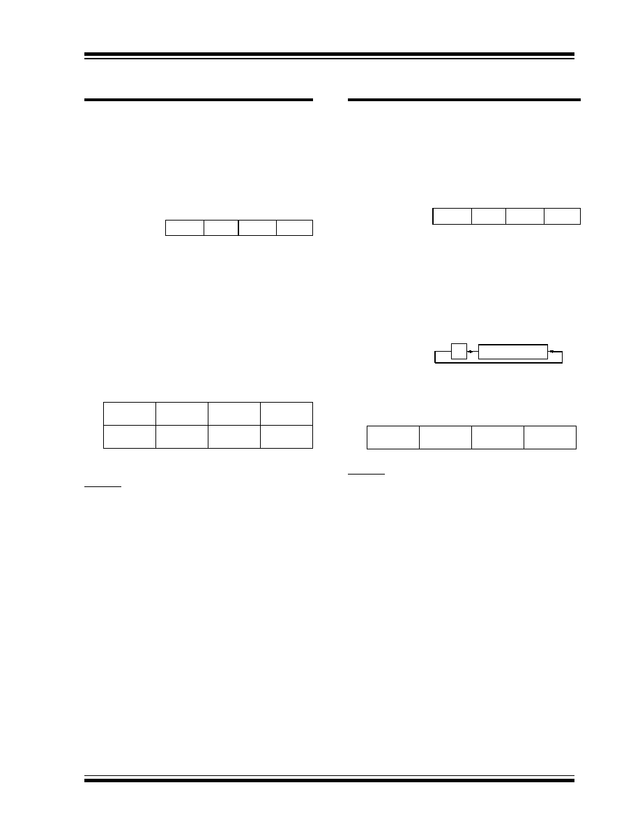
2002 Microchip Technology Inc.
DS41159B-page 309
PIC18FXX8
RETURN
Return from Subroutine
Syntax:
[ label ] RETURN [s]
Operands:
s
[0,1]
Operation:
(TOS)
PC,
if s = 1
(WS)
W,
(STATUSS)
STATUS,
(BSRS)
BSR,
PCLATU, PCLATH are unchanged
Status Affected:
None
Encoding:
0000
0000
0001
001s
Description:
Return from subroutine. The stack
is popped and the top of the stack
(TOS) is loaded into the program
counter. If `s'= 1, the contents of the
shadow registers WS, STATUSS
and BSRS are loaded into their cor-
responding registers, W, STATUS
and BSR. If `s' = 0, no update of
these registers occurs (default).
Words:
1
Cycles:
2
Q Cycle Activity:
Q1
Q2
Q3
Q4
Decode
No
operation
Process
Data
pop PC from
stack
No
operation
No
operation
No
operation
No
operation
Example:
RETURN
After Interrupt
PC = TOS
RLCF
Rotate Left f through Carry
Syntax:
[ label ] RLCF f [,d [,a]]
Operands:
0
f
255
d
[0,1]
a
[0,1]
Operation:
(f<n>)
dest<n+1>,
(f<7>)
C,
(C)
dest<0>
Status Affected:
C, N, Z
Encoding:
0011
01da
ffff
ffff
Description:
The contents of register 'f' are
rotated one bit to the left through
the Carry Flag. If 'd' is 0, the result
is placed in W. If 'd' is 1, the result
is stored back in register 'f'
(default). If `a' is 0, the Access
Bank will be selected, overriding
the BSR value. If 'a' = 1, then the
bank will be selected as per the
BSR value (default).
Words:
1
Cycles:
1
Q Cycle Activity:
Q1
Q2
Q3
Q4
Decode
Read
register 'f'
Process
Data
Write to
destination
Example:
RLCF
REG, W
Before Instruction
REG
=
1110 0110
C
=
0
After Instruction
REG
=
1110 0110
W
=
1100 1100
C
=
1
C
register f
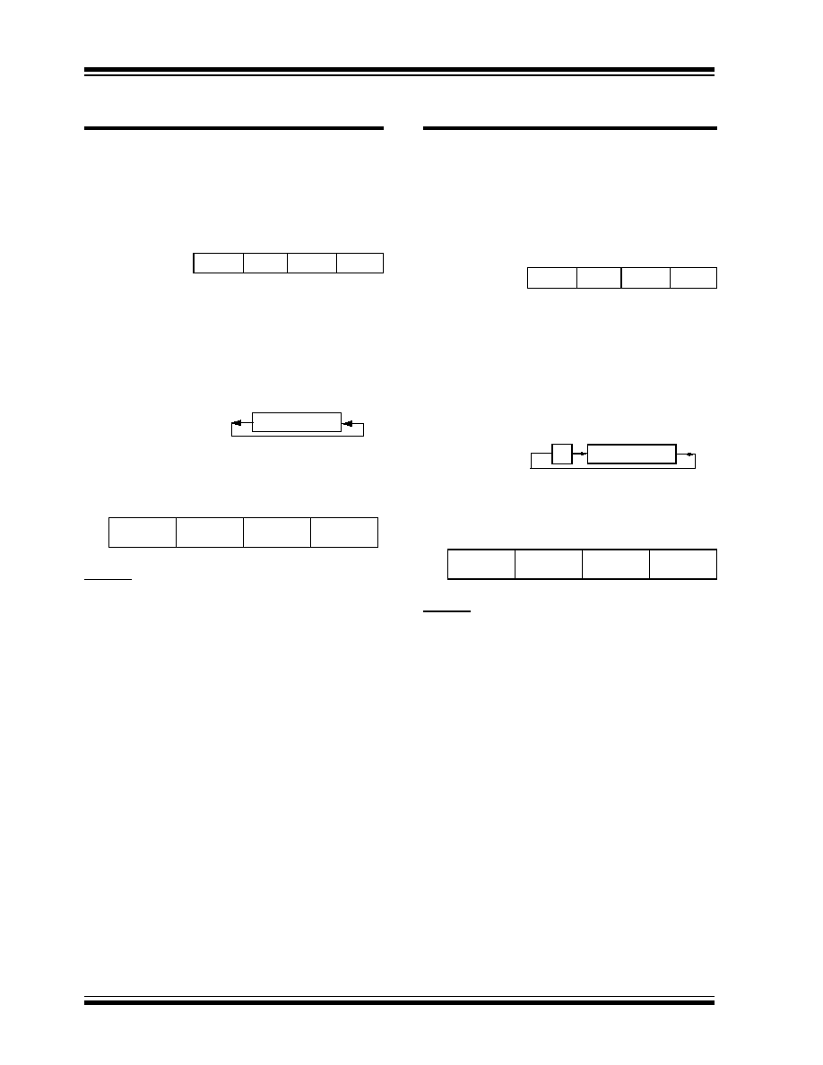
PIC18FXX8
DS41159B-page 310
2002 Microchip Technology Inc.
RLNCF
Rotate Left f (no carry)
Syntax:
[ label ] RLNCF f [,d [,a]]
Operands:
0
f
255
d
[0,1]
a
[0,1]
Operation:
(f<n>)
dest<n+1>,
(f<7>)
dest<0>
Status Affected:
N, Z
Encoding:
0100
01da
ffff
ffff
Description:
The contents of register 'f' are
rotated one bit to the left. If 'd' is 0,
the result is placed in W. If 'd' is 1,
the result is stored back in register
'f' (default). If 'a' is 0, the Access
Bank will be selected, overriding
the BSR value. If 'a' is 1, then the
bank will be selected as per the
BSR value (default).
Words:
1
Cycles:
1
Q Cycle Activity:
Q1
Q2
Q3
Q4
Decode
Read
register 'f'
Process
Data
Write to
destination
Example:
RLNCF
REG
Before Instruction
REG
=
1010 1011
After Instruction
REG
=
0101 0111
register f
RRCF
Rotate Right f through Carry
Syntax:
[ label ] RRCF f [,d [,a]]
Operands:
0
f
255
d
[0,1]
a
[0,1]
Operation:
(f<n>)
dest<n-1>,
(f<0>)
C,
(C)
dest<7>
Status Affected:
C, N, Z
Encoding:
0011
00da
ffff
ffff
Description:
The contents of register 'f' are
rotated one bit to the right through
the Carry Flag. If 'd' is 0, the result
is placed in W. If 'd' is 1, the result
is placed back in register 'f'
(default). If `a' is 0, the Access
Bank will be selected, overriding
the BSR value. If 'a' is 1, then the
bank will be selected as per the
BSR value (default).
Words:
1
Cycles:
1
Q Cycle Activity:
Q1
Q2
Q3
Q4
Decode
Read
register 'f'
Process
Data
Write to
destination
Example:
RRCF
REG, W
Before Instruction
REG
=
1110 0110
C
=
0
After Instruction
REG
=
1110 0110
W
=
0111 0011
C
=
0
C
register f
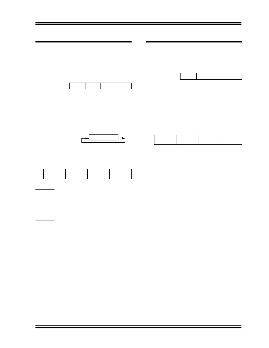
2002 Microchip Technology Inc.
DS41159B-page 311
PIC18FXX8
RRNCF
Rotate Right f (no carry)
Syntax:
[ label ] RRNCF f [,d [,a]]
Operands:
0
f
255
d
[0,1]
a
[0,1]
Operation:
(f<n>)
dest<n-1>,
(f<0>)
dest<7>
Status Affected:
N, Z
Encoding:
0100
00da
ffff
ffff
Description:
The contents of register 'f' are
rotated one bit to the right. If 'd' is 0,
the result is placed in W. If 'd' is 1,
the result is placed back in register
'f' (default). If 'a' is 0, the Access
Bank will be selected, overriding
the BSR value. If 'a' is 1, then the
bank will be selected as per the
BSR value (default).
Words:
1
Cycles:
1
Q Cycle Activity:
Q1
Q2
Q3
Q4
Decode
Read
register 'f'
Process
Data
Write to
destination
Example 1:
RRNCF REG, 1, 0
Before Instruction
REG
=
1101 0111
After Instruction
REG
=
1110 1011
Example 2:
RRNCF REG, W
Before Instruction
W
=
?
REG
=
1101 0111
After Instruction
W
=
1110 1011
REG
=
1101 0111
register f
SETF
Set f
Syntax:
[ label ] SETF f [,a]
Operands:
0
f
255
a
[0,1]
Operation:
FFh
f
Status Affected:
None
Encoding:
0110
100a
ffff
ffff
Description:
The contents of the specified regis-
ter are set to FFh. If 'a' is 0, the
Access Bank will be selected, over-
riding the BSR value. If 'a' is 1, then
the bank will be selected as per the
BSR value (default).
Words:
1
Cycles:
1
Q Cycle Activity:
Q1
Q2
Q3
Q4
Decode
Read
register 'f'
Process
Data
Write
register 'f'
Example:
SETF
REG
Before Instruction
REG
=
0x5A
After Instruction
REG
=
0xFF
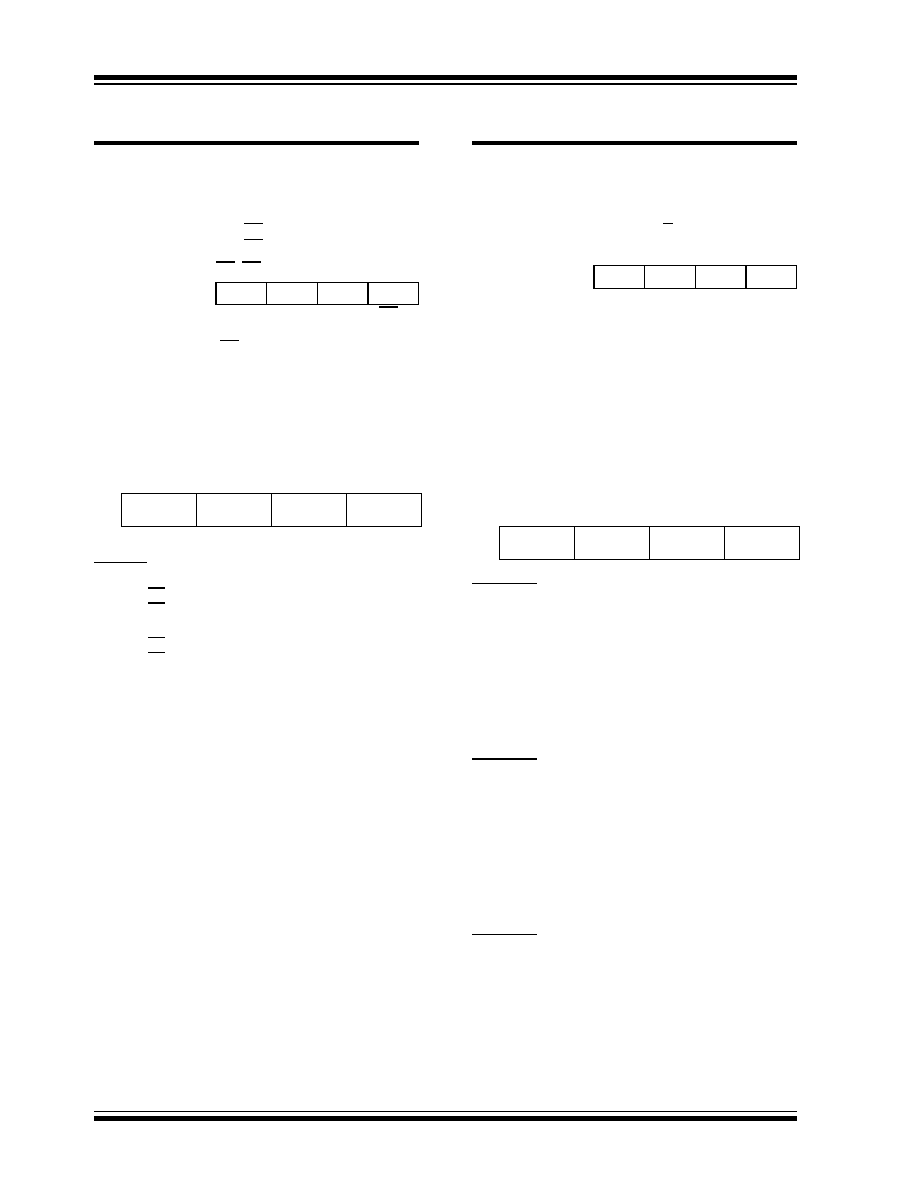
PIC18FXX8
DS41159B-page 312
2002 Microchip Technology Inc.
SLEEP
Enter SLEEP mode
Syntax:
[ label ] SLEEP
Operands:
None
Operation:
00h
WDT,
0
WDT postscaler,
1
TO,
0
PD
Status Affected:
TO, PD
Encoding:
0000
0000
0000
0011
Description:
The power-down status bit (PD) is
cleared. The time-out status bit
(TO) is set. Watchdog Timer and
its postscaler are cleared.
The processor is put into SLEEP
mode with the oscillator stopped.
Words:
1
Cycles:
1
Q Cycle Activity:
Q1
Q2
Q3
Q4
Decode
No
operation
Process
Data
Go to
sleep
Example:
SLEEP
Before Instruction
TO =
?
PD =
?
After Instruction
TO =
1
PD =
0
If WDT causes wake-up, this bit is cleared.
SUBFWB
Subtract f from W with borrow
Syntax:
[ label ] SUBFWB f [,d [,a]]
Operands:
0
f
255
d
[0,1]
a
[0,1]
Operation:
(W) � (f) � (C)
dest
Status Affected:
N, OV, C, DC, Z
Encoding:
0101
01da
ffff
ffff
Description:
Subtract register 'f' and carry flag
(borrow) from W (2's complement
method). If 'd' is 0, the result is
stored in W. If 'd' is 1, the result is
stored in register 'f' (default). If 'a' is
0, the Access Bank will be selected,
overriding the BSR value. If 'a' is 1,
then the bank will be selected as
per the BSR value (default).
Words:
1
Cycles:
1
Q Cycle Activity:
Q1
Q2
Q3
Q4
Decode
Read
register 'f'
Process
Data
Write to
destination
Example 1:
SUBFWB REG
Before Instruction
REG
=
0x03
W
=
0x02
C
=
0x01
After Instruction
REG
=
0xFF
W
=
0x02
C
=
0x00
Z
=
0x00
N
=
0x01 ; result is negative
Example 2:
SUBFWB REG, 0, 0
Before Instruction
REG
=
2
W
=
5
C
=
1
After Instruction
REG
=
2
W
=
3
C
=
1
Z
=
0
N
=
0 ; result is positive
Example 3:
SUBFWB REG, 1, 0
Before Instruction
REG
=
1
W
=
2
C
=
0
After Instruction
REG
=
0
W
=
2
C
=
1
Z
=
1 ; result is zero
N
=
0
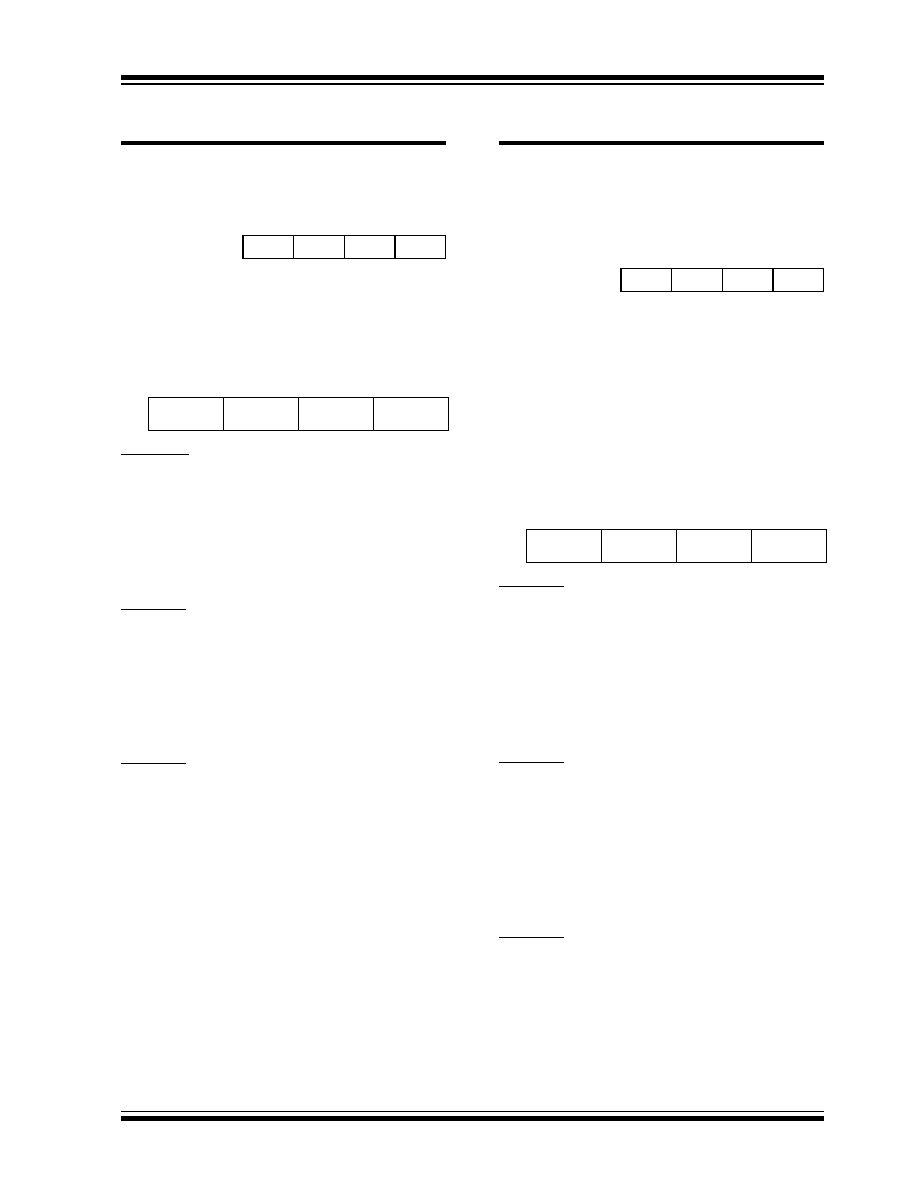
2002 Microchip Technology Inc.
DS41159B-page 313
PIC18FXX8
SUBLW
Subtract W from literal
Syntax:
[ label ] SUBLW k
Operands:
0
k
255
Operation:
k � (W)
W
Status Affected:
N, OV, C, DC, Z
Encoding:
0000
1000
kkkk
kkkk
Description:
W is subtracted from the eight-bit
literal 'k'. The result is placed in
W.
Words:
1
Cycles:
1
Q Cycle Activity:
Q1
Q2
Q3
Q4
Decode
Read
literal 'k'
Process
Data
Write to W
Example 1:
SUBLW
0x02
Before Instruction
W
=
1
C
=
?
After Instruction
W
=
1
C
=
1 ; result is positive
Z
=
0
N
=
0
Example 2:
SUBLW
0x02
Before Instruction
W
=
2
C
=
?
After Instruction
W
=
0
C
=
1 ; result is zero
Z
=
1
N
=
0
Example 3:
SUBLW
0x02
Before Instruction
W
=
3
C
=
?
After Instruction
W
=
FF ; (2's complement)
C
=
0 ; result is negative
Z
=
0
N
=
1
SUBWF
Subtract W from f
Syntax:
[ label ] SUBWF f [,d [,a]]
Operands:
0
f
255
d
[0,1]
a
[0,1]
Operation:
(f) � (W)
dest
Status Affected:
N, OV, C, DC, Z
Encoding:
0101
11da
ffff
ffff
Description:
Subtract W from register 'f' (2's
complement method). If 'd' is 0,
the result is stored in W. If 'd' is 1,
the result is stored back in regis-
ter 'f' (default). If 'a' is 0, the
Access Bank will be selected,
overriding the BSR value. If 'a' is
1, then the bank will be selected
as per the BSR value (default).
Words:
1
Cycles:
1
Q Cycle Activity:
Q1
Q2
Q3
Q4
Decode
Read
register 'f'
Process
Data
Write to
destination
Example 1:
SUBWF REG
Before Instruction
REG
=
3
W
=
2
C
=
?
After Instruction
REG
=
1
W
=
2
C
=
1 ; result is positive
Z
=
0
N
=
0
Example 2:
SUBWF REG, W
Before Instruction
REG
=
2
W
=
2
C
=
?
After Instruction
REG
=
2
W
=
0
C
=
1 ; result is zero
Z
=
1
N
=
0
Example 3:
SUBWF REG
Before Instruction
REG
=
0x01
W
=
0x02
C
=
?
After Instruction
REG
=
0xFFh ;(2's complement)
W
=
0x02
C
=
0x00 ; result is negative
Z
=
0x00
N
=
0x01

PIC18FXX8
DS41159B-page 314
2002 Microchip Technology Inc.
SUBWFB
Subtract W from f with Borrow
Syntax:
[ label ] SUBWFB f [,d [,a]]
Operands:
0
f
255
d
[0,1]
a
[0,1]
Operation:
(f) � (W) � (C)
dest
Status Affected:
N, OV, C, DC, Z
Encoding:
0101
10da
ffff
ffff
Description:
Subtract W and the carry flag (bor-
row) from register 'f' (2's complement
method). If 'd' is 0, the result is stored
in W. If 'd' is 1, the result is stored
back in register 'f' (default). If 'a' is 0,
the Access Bank will be selected,
overriding the BSR value. If 'a' is 1,
then the bank will be selected as per
the BSR value (default).
Words:
1
Cycles:
1
Q Cycle Activity:
Q1
Q2
Q3
Q4
Decode
Read
register 'f'
Process
Data
Write to
destination
Example 1:
SUBWFB REG, 1, 0
Before Instruction
REG
=
0x19
(0001 1001)
W
=
0x0D
(0000 1101)
C
=
0x01
After Instruction
REG
=
0x0C
(0000 1011)
W
=
0x0D
(0000 1101)
C
=
0x01
Z
=
0x00
N
=
0x00
; result is positive
Example 2:
SUBWFB
REG, 0, 0
Before Instruction
REG
=
0x1B
(0001 1011)
W
=
0x1A
(0001 1010)
C
=
0x00
After Instruction
REG
=
0x1B
(0001 1011)
W
=
0x00
C
=
0x01
Z
=
0x01
; result is zero
N
=
0x00
Example 3:
SUBWFB REG, 1, 0
Before Instruction
REG
=
0x03
(0000 0011)
W
=
0x0E
(0000 1101)
C
=
0x01
After Instruction
REG
=
0xF5
(1111 0100)
; [2's comp]
W
=
0x0E
(0000 1101)
C
=
0x00
Z
=
0x00
N
=
0x01
; result is negative
SWAPF
Swap f
Syntax:
[ label ] SWAPF f [,d [,a]]
Operands:
0
f
255
d
[0,1]
a
[0,1]
Operation:
(f<3:0>)
dest<7:4>,
(f<7:4>)
dest<3:0>
Status Affected:
None
Encoding:
0011
10da
ffff
ffff
Description:
The upper and lower nibbles of reg-
ister 'f' are exchanged. If 'd' is 0, the
result is placed in W. If 'd' is 1, the
result is placed in register 'f'
(default). If 'a' is 0, the Access
Bank will be selected, overriding
the BSR value. If 'a' is 1, then the
bank will be selected as per the
BSR value (default).
Words:
1
Cycles:
1
Q Cycle Activity:
Q1
Q2
Q3
Q4
Decode
Read
register 'f'
Process
Data
Write to
destination
Example:
SWAPF
REG
Before Instruction
REG
=
0x53
After Instruction
REG
=
0x35

2002 Microchip Technology Inc.
DS41159B-page 315
PIC18FXX8
TBLRD
Table Read
Syntax:
[ label ]
TBLRD ( *; *+; *-; +*)
Operands:
None
Operation:
if TBLRD *,
(Prog Mem (TBLPTR))
TABLAT;
TBLPTR - No Change;
if TBLRD *+,
(Prog Mem (TBLPTR))
TABLAT;
(TBLPTR) +1
TBLPTR;
if TBLRD *-,
(Prog Mem (TBLPTR))
TABLAT;
(TBLPTR) -1
TBLPTR;
if TBLRD +*,
(TBLPTR) +1
TBLPTR;
(Prog Mem (TBLPTR))
TABLAT;
Status Affected:None
Encoding:
0000
0000
0000
10nn
nn=0 *
=1 *+
=2 *-
=3 +*
Description:
This instruction is used to read the con-
tents of Program Memory (P.M.). To
address the program memory, a pointer
called Table Pointer (TBLPTR) is used.
The TBLPTR (a 21-bit pointer) points
to each byte in the program memory.
TBLPTR has a 2 Mbyte address range.
TBLPTR[0] = 0: Least Significant
Byte of Program
Memory Word
TBLPTR[0] = 1: Most Significant
Byte of Program
Memory Word
The
TBLRD
instruction can modify the
value of TBLPTR as follows:
� no change
� post-increment
� post-decrement
� pre-increment
Words:
1
Cycles:
2
Q Cycle Activity:
Q1
Q2
Q3
Q4
Decode
No
operation
No
operation
No
operation
No
operation
No operation
(Read Program
Memory)
No
operation
No operation
(Write TABLAT)
TBLRD
Table Read (cont'd)
Example1:
TBLRD *+ ;
Before Instruction
TABLAT
=
0x55
TBLPTR
=
0x00A356
MEMORY(0x00A356)
=
0x34
After Instruction
TABLAT
=
0x34
TBLPTR
=
0x00A357
Example2:
TBLRD +* ;
Before Instruction
TABLAT
=
0xAA
TBLPTR
=
0x01A357
MEMORY(0x01A357)
=
0x12
MEMORY(0x01A358)
=
0x34
After Instruction
TABLAT
=
0x34
TBLPTR
=
0x01A358

PIC18FXX8
DS41159B-page 316
2002 Microchip Technology Inc.
TBLWT Table
Write
Syntax:
[ label ]
TBLWT ( *; *+; *-; +*)
Operands:
None
Operation:
if TBLWT*,
(TABLAT)
Holding Register;
TBLPTR - No Change;
if TBLWT*+,
(TABLAT)
Holding Register;
(TBLPTR) +1
TBLPTR;
if TBLWT*-,
(TABLAT)
Holding Register;
(TBLPTR) -1
TBLPTR;
if TBLWT+*,
(TBLPTR) +1
TBLPTR;
(TABLAT)
Holding Register;
Status Affected: None
Encoding:
0000
0000
0000
11nn
nn=0 *
=1 *+
=2 *-
=3 +*
Description:
This instruction uses the 3 LSBs of
TBLPTR to determine which of the 8
holding registers the TABLAT is written
to. The holding registers are used to
program the contents of Program
Memory (P.M.). (Refer to Section 6.0
for additional details on programming
FLASH memory.)
The TBLPTR (a 21-bit pointer) points
to each byte in the program memory.
TBLPTR has a 2 MBtye address
range. The LSb of the TBLPTR selects
which byte of the program memory
location to access.
TBLPTR[0] = 0: Least Significant
Byte of Program
Memory Word
TBLPTR[0] = 1: Most Significant
Byte of Program
Memory Word
The
TBLWT
instruction can modify the
value of TBLPTR as follows:
� no change
� post-increment
� post-decrement
� pre-increment
TBLWT Table Write (Continued)
Words: 1
Cycles: 2
Q Cycle Activity:
Q1
Q2
Q3
Q4
Decode
No
operation
No
operation
No
operation
No
operation
No
operation
(Read
TABLAT)
No
operation
No
operation
(Write to
Holding
Register )
Example1:
TBLWT *+;
Before Instruction
TABLAT =
0x55
TBLPTR
=
0x00A356
HOLDING REGISTER
(0x00A356)
=
0xFF
After Instructions (table write completion)
TABLAT
=
0x55
TBLPTR
=
0x00A357
HOLDING REGISTER
(0x00A356)
=
0x55
Example 2:
TBLWT +*;
Before Instruction
TABLAT
=
0x34
TBLPTR
=
0x01389A
HOLDING REGISTER
(0x01389A)
=
0xFF
HOLDING REGISTER
(0x01389B)
=
0xFF
After Instruction (table write completion)
TABLAT
=
0x34
TBLPTR
=
0x01389B
HOLDING REGISTER
(0x01389A)
=
0xFF
HOLDING REGISTER
(0x01389B)
=
0x34
2002 Microchip Technology Inc.
DS41159B-page 317
PIC18FXX8
TSTFSZ
Test f, skip if 0
Syntax:
[ label ] TSTFSZ f [,a]
Operands:
0
f
255
a
[0,1]
Operation:
skip if f = 0
Status Affected:
None
Encoding:
0110
011a
ffff
ffff
Description:
If 'f' = 0, the next instruction,
fetched during the current instruc-
tion execution is discarded and a
NOP
is executed, making this a
two-cycle instruction. If 'a' is 0, the
Access Bank will be selected, over-
riding the BSR value. If 'a' is 1,
then the bank will be selected as
per the BSR value (default).
Words:
1
Cycles:
1(2)
Note: 3 cycles if skip and followed
by a 2-word instruction.
Q Cycle Activity:
Q1
Q2
Q3
Q4
Decode
Read
register 'f'
Process
Data
No
operation
If skip:
Q1
Q2
Q3
Q4
No
operation
No
operation
No
operation
No
operation
If skip and followed by 2-word instruction:
Q1
Q2
Q3
Q4
No
operation
No
operation
No
operation
No
operation
No
operation
No
operation
No
operation
No
operation
Example:
HERE TSTFSZ CNT
NZERO :
ZERO :
Before Instruction
PC =
Address
(HERE)
After Instruction
If CNT
=
0x00,
PC =
Address
(ZERO)
If CNT
0x00,
PC =
Address
(NZERO)
XORLW
Exclusive OR literal with W
Syntax:
[ label ] XORLW k
Operands:
0
k
255
Operation:
(W) .XOR. k
W
Status Affected:
N, Z
Encoding:
0000
1010
kkkk
kkkk
Description:
The contents of W are XORed
with the 8-bit literal 'k'. The result
is placed in W.
Words:
1
Cycles:
1
Q Cycle Activity:
Q1
Q2
Q3
Q4
Decode
Read
literal 'k'
Process
Data
Write to W
Example:
XORLW
0xAF
Before Instruction
W
=
0xB5
After Instruction
W
=
0x1A

PIC18FXX8
DS41159B-page 318
2002 Microchip Technology Inc.
XORWF
Exclusive OR W with f
Syntax:
[ label ] XORWF f [,d [,a]]
Operands:
0
f
255
d
[0,1]
a
[0,1]
Operation:
(W) .XOR. (f)
dest
Status Affected:
N, Z
Encoding:
0001
10da
ffff
ffff
Description:
Exclusive OR the contents of W
with register 'f'. If 'd' is 0, the result
is stored in W. If 'd' is 1, the result is
stored back in the register 'f'
(default). If `a' is 0, the Access
Bank will be selected, overriding
the BSR value. If 'a' is 1, then the
bank will be selected as per the
BSR value (default).
Words:
1
Cycles:
1
Q Cycle Activity:
Q1
Q2
Q3
Q4
Decode
Read
register 'f'
Process
Data
Write to
destination
Example:
XORWF REG
Before Instruction
REG
=
0xAF
W
=
0xB5
After Instruction
REG
=
0x1A
W
=
0xB5

2002 Microchip Technology Inc.
Preliminary
DS41159B-page 319
PIC18FXX8
26.0
DEVELOPMENT SUPPORT
The PICmicro
�
microcontrollers are supported with a
full range of hardware and software development tools:
� Integrated Development Environment
- MPLAB
�
IDE Software
� Assemblers/Compilers/Linkers
- MPASM
TM
Assembler
- MPLAB C17 and MPLAB C18 C Compilers
- MPLINK
TM
Object Linker/
MPLIB
TM
Object Librarian
� Simulators
- MPLAB SIM Software Simulator
� Emulators
- MPLAB ICE 2000 In-Circuit Emulator
- ICEPICTM In-Circuit Emulator
� In-Circuit Debugger
- MPLAB ICD
� Device Programmers
- PRO MATE
�
II Universal Device Programmer
- PICSTART
�
Plus Entry-Level Development
Programmer
� Low Cost Demonstration Boards
- PICDEM
TM
1 Demonstration Board
- PICDEM 2 Demonstration Board
- PICDEM
3 Demonstration Board
- PICDEM
17 Demonstration Board
- K
EE
L
OQ
�
Demonstration Board
26.1
MPLAB Integrated Development
Environment Software
The MPLAB IDE software brings an ease of software
development previously unseen in the 8-bit microcon-
troller market. The MPLAB IDE is a Windows
�
-based
application that contains:
� An interface to debugging tools
- simulator
- programmer (sold separately)
- emulator (sold separately)
- in-circuit debugger (sold separately)
� A full-featured editor
� A project manager
� Customizable toolbar and key mapping
� A status bar
� On-line help
The MPLAB IDE allows you to:
� Edit your source files (either assembly or `C')
� One touch assemble (or compile) and download
to PICmicro emulator and simulator tools (auto-
matically updates all project information)
� Debug using:
- source files
- absolute listing file
- machine code
The ability to use MPLAB IDE with multiple debugging
tools allows users to easily switch from the cost-
effective simulator to a full-featured emulator with
minimal retraining.
26.2
MPASM Assembler
The MPASM assembler is a full-featured universal
macro assembler for all PICmicro MCU's.
The MPASM assembler has a command line interface
and a Windows shell. It can be used as a stand-alone
application on a Windows 3.x or greater system, or it
can be used through MPLAB IDE. The MPASM assem-
bler generates relocatable object files for the MPLINK
object linker, Intel
�
standard HEX files, MAP files to
detail memory usage and symbol reference, an abso-
lute LST file that contains source lines and generated
machine code, and a COD file for debugging.
The MPASM assembler features include:
� Integration into MPLAB IDE projects.
� User-defined macros to streamline assembly
code.
� Conditional assembly for multi-purpose source
files.
� Directives that allow complete control over the
assembly process.
26.3
MPLAB C17 and MPLAB C18
C Compilers
The MPLAB C17 and MPLAB C18 Code Development
Systems are complete ANSI `C' compilers for
Microchip's PIC17CXXX and PIC18CXXX family of
microcontrollers, respectively. These compilers provide
powerful integration capabilities and ease of use not
found with other compilers.
For easier source level debugging, the compilers pro-
vide symbol information that is compatible with the
MPLAB IDE memory display.

PIC18FXX8
DS41159B-page 320
Preliminary
2002 Microchip Technology Inc.
26.4
MPLINK Object Linker/
MPLIB Object Librarian
The MPLINK object linker combines relocatable
objects created by the MPASM assembler and the
MPLAB C17 and MPLAB C18 C compilers. It can also
link relocatable objects from pre-compiled libraries,
using directives from a linker script.
The MPLIB object librarian is a librarian for pre-
compiled code to be used with the MPLINK object
linker. When a routine from a library is called from
another source file, only the modules that contain that
routine will be linked in with the application. This allows
large libraries to be used efficiently in many different
applications. The MPLIB object librarian manages the
creation and modification of library files.
The MPLINK object linker features include:
� Integration with MPASM assembler and MPLAB
C17 and MPLAB C18 C compilers.
� Allows all memory areas to be defined as sections
to provide link-time flexibility.
The MPLIB object librarian features include:
� Easier linking because single libraries can be
included instead of many smaller files.
� Helps keep code maintainable by grouping
related modules together.
� Allows libraries to be created and modules to be
added, listed, replaced, deleted or extracted.
26.5
MPLAB SIM Software Simulator
The MPLAB SIM software simulator allows code devel-
opment in a PC-hosted environment by simulating the
PICmicro series microcontrollers on an instruction
level. On any given instruction, the data areas can be
examined or modified and stimuli can be applied from
a file, or user-defined key press, to any of the pins. The
execution can be performed in single step, execute
until break, or trace mode.
The MPLAB SIM simulator fully supports symbolic debug-
ging using the MPLAB C17 and the MPLAB C18 C com-
pilers and the MPASM assembler. The software simulator
offers the flexibility to develop and debug code outside of
the laboratory environment, making it an excellent multi-
project software development tool.
26.6
MPLAB ICE High Performance
Universal In-Circuit Emulator with
MPLAB IDE
The MPLAB ICE universal in-circuit emulator is intended
to provide the product development engineer with a
complete microcontroller design tool set for PICmicro
microcontrollers (MCUs). Software control of the
MPLAB ICE in-circuit emulator is provided by the
MPLAB Integrated Development Environment (IDE),
which allows editing, building, downloading and source
debugging from a single environment.
The MPLAB ICE 2000 is a full-featured emulator sys-
tem with enhanced trace, trigger and data monitoring
features. Interchangeable processor modules allow the
system to be easily reconfigured for emulation of differ-
ent processors. The universal architecture of the
MPLAB ICE in-circuit emulator allows expansion to
support new PICmicro microcontrollers.
The MPLAB ICE in-circuit emulator system has been
designed as a real-time emulation system, with
advanced features that are generally found on more
expensive development tools. The PC platform and
Microsoft
�
Windows environment were chosen to best
make these features available to you, the end user.
26.7
ICEPIC In-Circuit Emulator
The ICEPIC low cost, in-circuit emulator is a solution
for the Microchip Technology PIC16C5X, PIC16C6X,
PIC16C7X and PIC16CXXX families of 8-bit One-
Time-Programmable (OTP) microcontrollers. The mod-
ular system can support different subsets of PIC16C5X
or PIC16CXXX products through the use of inter-
changeable personality modules, or daughter boards.
The emulator is capable of emulating without target
application circuitry being present.

2002 Microchip Technology Inc.
Preliminary
DS41159B-page 321
PIC18FXX8
26.8
MPLAB ICD In-Circuit Debugger
Microchip's In-Circuit Debugger, MPLAB ICD, is a pow-
erful, low cost, run-time development tool. This tool is
based on the FLASH PICmicro MCUs and can be used
to develop for this and other PICmicro microcontrollers.
The MPLAB ICD utilizes the in-circuit debugging capa-
bility built into the FLASH devices. This feature, along
with Microchip's In-Circuit Serial Programming
TM
proto-
col, offers cost-effective in-circuit FLASH debugging
from the graphical user interface of the MPLAB
Integrated Development Environment. This enables a
designer to develop and debug source code by watch-
ing variables, single-stepping and setting break points.
Running at full speed enables testing hardware in real-
time.
26.9
PRO MATE II Universal Device
Programmer
The PRO MATE II universal device programmer is a
full-featured programmer, capable of operating in
stand-alone mode, as well as PC-hosted mode. The
PRO MATE II device programmer is CE compliant.
The PRO MATE II device programmer has program-
mable V
DD
and V
PP
supplies, which allow it to verify
programmed memory at V
DD
min and V
DD
max for max-
imum reliability. It has an LCD display for instructions
and error messages, keys to enter commands and a
modular detachable socket assembly to support various
package types. In stand-alone mode, the PRO MATE II
device programmer can read, verify, or program
PICmicro devices. It can also set code protection in this
mode.
26.10 PICSTART Plus Entry Level
Development Programmer
The PICSTART Plus development programmer is an
easy-to-use, low cost, prototype programmer. It con-
nects to the PC via a COM (RS-232) port. MPLAB
Integrated Development Environment software makes
using the programmer simple and efficient.
The PICSTART Plus development programmer sup-
ports all PICmicro devices with up to 40 pins. Larger pin
count devices, such as the PIC16C92X and
PIC17C76X, may be supported with an adapter socket.
The PICSTART Plus development programmer is CE
compliant.
26.11 PICDEM 1 Low Cost PICmicro
Demonstration Board
The PICDEM 1 demonstration board is a simple board
which demonstrates the capabilities of several of
Microchip's microcontrollers. The microcontrollers sup-
ported are: PIC16C5X (PIC16C54 to PIC16C58A),
PIC16C61, PIC16C62X, PIC16C71, PIC16C8X,
PIC17C42, PIC17C43 and PIC17C44. All necessary
hardware and software is included to run basic demo
programs. The user can program the sample microcon-
trollers provided with the PICDEM 1 demonstration
board on a PRO MATE II device programmer, or a
PICSTART Plus development programmer, and easily
test firmware. The user can also connect the
PICDEM 1 demonstration board to the MPLAB ICE in-
circuit emulator and download the firmware to the emu-
lator for testing. A prototype area is available for the
user to build some additional hardware and connect it
to the microcontroller socket(s). Some of the features
include an RS-232 interface, a potentiometer for simu-
lated analog input, push button switches and eight
LEDs connected to PORTB.
26.12 PICDEM 2 Low Cost PIC16CXX
Demonstration Board
The PICDEM 2 demonstration board is a simple dem-
onstration board that supports the PIC16C62,
PIC16C64, PIC16C65, PIC16C73 and PIC16C74
microcontrollers. All the necessary hardware and soft-
ware is included to run the basic demonstration pro-
grams. The user can program the sample
microcontrollers provided with the PICDEM 2 demon-
stration board on a PRO MATE II device programmer,
or a PICSTART Plus development programmer, and
easily test firmware. The MPLAB ICE in-circuit emula-
tor may also be used with the PICDEM 2 demonstration
board to test firmware. A prototype area has been pro-
vided to the user for adding additional hardware and
connecting it to the microcontroller socket(s). Some of
the features include a RS-232 interface, push button
switches, a potentiometer for simulated analog input, a
serial EEPROM to demonstrate usage of the I
2
C
TM
bus
and separate headers for connection to an LCD
module and a keypad.

PIC18FXX8
DS41159B-page 322
Preliminary
2002 Microchip Technology Inc.
26.13 PICDEM 3 Low Cost PIC16CXXX
Demonstration Board
The PICDEM 3 demonstration board is a simple dem-
onstration board that supports the PIC16C923 and
PIC16C924 in the PLCC package. It will also support
future 44-pin PLCC microcontrollers with an LCD Mod-
ule. All the necessary hardware and software is
included to run the basic demonstration programs. The
user can program the sample microcontrollers pro-
vided with the PICDEM 3 demonstration board on a
PRO MATE II device programmer, or a PICSTART Plus
development programmer with an adapter socket, and
easily test firmware. The MPLAB ICE in-circuit emula-
tor may also be used with the PICDEM 3 demonstration
board to test firmware. A prototype area has been pro-
vided to the user for adding hardware and connecting it
to the microcontroller socket(s). Some of the features
include a RS-232 interface, push button switches, a
potentiometer for simulated analog input, a thermistor
and separate headers for connection to an external
LCD module and a keypad. Also provided on the
PICDEM 3 demonstration board is a LCD panel, with 4
commons and 12 segments, that is capable of display-
ing time, temperature and day of the week. The
PICDEM 3 demonstration board provides an additional
RS-232 interface and Windows software for showing
the demultiplexed LCD signals on a PC. A simple serial
interface allows the user to construct a hardware
demultiplexer for the LCD signals.
26.14 PICDEM 17 Demonstration Board
The PICDEM 17 demonstration board is an evaluation
board that demonstrates the capabilities of several
Microchip microcontrollers, including PIC17C752,
PIC17C756A, PIC17C762 and PIC17C766. All neces-
sary hardware is included to run basic demo programs,
which are supplied on a 3.5-inch disk. A programmed
sample is included and the user may erase it and
program it with the other sample programs using the
PRO MATE II device programmer, or the PICSTART
Plus development programmer, and easily debug and
test the sample code. In addition, the PICDEM 17 dem-
onstration board supports downloading of programs to
and executing out of external FLASH memory on board.
The PICDEM 17 demonstration board is also usable
with the MPLAB ICE in-circuit emulator, or the
PICMASTER emulator and all of the sample programs
can be run and modified using either emulator. Addition-
ally, a generous prototype area is available for user
hardware.
26.15 K
EE
L
OQ
Evaluation and
Programming Tools
K
EE
L
OQ
evaluation and programming tools support
Microchip's HCS Secure Data Products. The HCS eval-
uation kit includes a LCD display to show changing
codes, a decoder to decode transmissions and a pro-
gramming interface to program test transmitters.

2002 Microchip Technology Inc.
Preliminary
DS41159B-page 323
PIC18FXX8
TABLE 26-1:
DEVELOPMENT TOOLS FROM MICROCHIP
PIC1
2C
XXX
PIC
14000
PIC
16C5
X
PIC
16C6
X
PIC1
6C
XXX
PIC
16F62
X
PIC
16C7
X
PIC
16C
7XX
PIC
16C8
X/
PIC
16F
8X
PIC
16F
8XX
PIC
16C
9XX
PIC
17C4
X
PIC
17C
7XX
PIC1
8C
XX2
PIC1
8F
XX
X
24C
XX
/
25C
XX
/
93C
XX
HCSXXX
MCRF
XXX
MCP
25
10
Soft
wa
re
Tool
s
MP
L
A
B
�
In
t
e
g
r
a
t
ed
D
e
ve
l
o
p
m
en
t E
n
vi
r
onm
en
t
9
9
9
9
9
9
9
9
9
9
9
9
9
9
9
MP
L
A
B
�
C1
7
C
Co
m
p
ile
r
9
9
MP
L
A
B
�
C1
8
C
Co
m
p
ile
r
9
9
MP
A
S
M
TM
Ass
e
m
b
le
r
/
MP
L
I
N
K
TM
Ob
je
ct L
i
n
k
e
r
9
9
9
9
9
9
9
9
9
9
9
9
9
9
9
9
9
Emul
ato
rs
MP
L
A
B
�
ICE
In
-Ci
r
c
u
it
E
m
u
l
at
o
r
9
9
9
9
9
9
**
9
9
9
9
9
9
9
9
9
I
C
EPI
C
TM
In
-Ci
r
c
u
it
E
m
u
l
a
t
o
r
9
9
9
9
9
9
9
9
De
bugg
er
MP
L
A
B
�
ICD
In
-Cir
cu
it
D
e
bu
gge
r
9
*
9
*
9
9
Progr
ammer
s
PICST
ART
�
Pl
u
s
En
t
r
y
Le
v
e
l
D
e
v
e
l
o
p
m
e
n
t Pr
og
ra
mme
r
9
9
9
9
9
9
**
9
9
9
9
9
9
9
9
9
PRO
M
A
T
E
�
II
U
n
i
ver
sa
l D
e
vic
e
P
r
og
r
a
m
m
e
r
9
9
9
9
9
9
**
9
9
9
9
9
9
9
9
9
9
9
Dem
o Bo
ard
s a
nd
Eva
l Ki
ts
PICDEM
TM
1
Dem
o
n
s
tr
at
io
n
Bo
a
r
d
9
9
9
9
9
PICDEM
TM
2
Dem
o
n
s
tr
at
io
n
Bo
a
r
d
9
9
9
9
PICDEM
TM
3
Dem
o
n
s
tr
at
io
n
Bo
a
r
d
9
PICDEM
TM
1
4
A De
m
o
n
s
t
r
a
t
io
n
Bo
a
r
d
9
PICDEM
TM
17
D
e
m
o
ns
tr
at
i
o
n
Bo
a
r
d
9
K
EE
L
OQ
�
Ev
a
l
ua
t
i
o
n
Ki
t
9
K
EE
L
OQ
�
Tr
an
sp
on
d
e
r
K
i
t
9
mi
c
r
o
I
D
TM
Pr
og
ra
mme
r
'
s K
i
t
9
12
5 k
H
z m
i
cr
o
I
D
TM
De
v
e
lo
p
e
r
'
s K
i
t
9
12
5 kH
z A
n
tic
o
l
lisi
o
n
m
i
c
r
oID
TM
De
v
e
lo
p
e
r
'
s K
i
t
9
13
.56 MH
z
A
n
tic
o
lli
sion
mi
c
r
oI
D
TM
D
e
v
e
l
oper
'
s K
i
t
9
M
C
P2
5
1
0
CAN De
v
e
lo
p
e
r
'
s K
i
t
9
*
C
ontact
the
Mi
cr
och
i
p T
e
chn
o
l
o
g
y
In
c. w
e
b si
t
e
a
t
w
w
w
.m
i
c
roc
h
i
p
.c
om
for
i
n
fo
rm
ati
o
n o
n
h
o
w
t
o
u
s
e t
he
MP
LA
B
�
IC
D
In
-C
i
r
cui
t
D
e
bu
gge
r (
D
V
164
00
1)
w
i
t
h P
I
C
1
6C
6
2
,
63,
64,
65
, 7
2
, 7
3
,
74,
76
, 77
.
*
*
Co
n
t
a
c
t
M
i
cr
o
c
h
i
p
T
e
c
h
n
o
lo
g
y
In
c.
fo
r
a
v
a
ila
b
ility
d
a
t
e
.
D
e
vel
o
pm
ent
too
l
i
s
av
ai
l
a
b
l
e on
se
l
e
ct d
e
vi
ce
s.

PIC18FXX8
DS41159B-page 324
Preliminary
2002 Microchip Technology Inc.
NOTES:

2002 Microchip Technology Inc.
Preliminary
DS41159B-page 325
PIC18FXX8
27.0
ELECTRICAL CHARACTERISTICS
Absolute Maximum Ratings
()
Ambient temperature under bias............................................................................................................ .-55�C to +125�C
Storage temperature .............................................................................................................................. -65�C to +150�C
Voltage on any pin with respect to V
SS
(except V
DD
, MCLR, and RA4) ......................................... -0.3V to (V
DD
+ 0.3V)
Voltage on V
DD
with respect to V
SS
......................................................................................................... -0.3V to +7.5V
Voltage on MCLR with respect to V
SS
(Note 2) ......................................................................................... 0V to +13.25V
Voltage on RA4 with respect to Vss ............................................................................................................... 0V to +8.5V
Total power dissipation (Note 1) ............................................................................................................................... 1.0W
Maximum current out of V
SS
pin ........................................................................................................................... 300 mA
Maximum current into V
DD
pin .............................................................................................................................. 250 mA
Input clamp current, I
IK
(V
I
< 0 or V
I
> V
DD
) .......................................................................................................... �20 mA
Output clamp current, I
OK
(V
O
< 0 or V
O
> V
DD
) ................................................................................................... �20 mA
Maximum output current sunk by any I/O pin..........................................................................................................25 mA
Maximum output current sourced by any I/O pin .................................................................................................... 25 mA
Maximum current sunk by all ports (combined) .................................................................................................... 200 mA
Maximum current sourced by all ports (combined) ............................................................................................... 200 mA
Note 1: Power dissipation is calculated as follows:
Pdis = V
DD
x {I
DD
-
I
OH
} +
{(V
DD
-V
OH
) x I
OH
} +
(V
O
l x I
OL
)
2: Voltage spikes below V
SS
at the MCLR/V
PP
pin, inducing currents greater than 80 mA, may cause latchup.
Thus, a series resistor of 50-100
should be used when applying a "low" level to the MCLR/V
PP
pin, rather
than pulling this pin directly to V
SS
.
Note:
Stresses above those listed under "Absolute Maximum Ratings" may cause permanent damage to the
device. This is a stress rating only and functional operation of the device at those or any other conditions
above those indicated in the operation listings of this specification is not implied. Exposure to maximum
rating conditions for extended periods may affect device reliability.
PIC18FXX8
DS41159B-page 326
Preliminary
2002 Microchip Technology Inc.
FIGURE 27-1:
PIC18FXX8 VOLTAGE-FREQUENCY GRAPH (INDUSTRIAL)
FIGURE 27-2:
PIC18LFXX8 VOLTAGE-FREQUENCY GRAPH (INDUSTRIAL)
Frequency
Vo
l
t
a
g
e
6.0V
5.5V
4.5V
4.0V
2.0V
40 MHz
5.0V
3.5V
3.0V
2.5V
PIC18FXX8
4.2V
Frequency
Vo
l
t
a
g
e
6.0V
5.5V
4.5V
4.0V
2.0V
40 MHz
5.0V
3.5V
3.0V
2.5V
PIC18LFXX8
4 MHz
4.2V
F
MAX
= (16.36 MHz/V) (V
DDAPPMIN
� 2.0V) + 4 MHz, if V
DDAPPMIN
4.2V
Note: V
DDAPPMIN
is the minimum voltage of the PICmicro
�
device in the application.
= 40 MHz, if V
DDAPPMIN
> 4.2V
2002 Microchip Technology Inc.
Preliminary
DS41159B-page 327
PIC18FXX8
27.1
DC Characteristics
PIC18LFXX8
(Industrial)
Standard Operating Conditions (unless otherwise stated)
Operating temperature
-40�C
T
A
+85�C for industrial
PIC18FXX8
(Industrial, Extended)
Standard Operating Conditions (unless otherwise stated)
Operating temperature
-40�C
T
A
+85�C for industrial
-40
�
C
T
A
+125�C for extended
Param
No.
Symbol
Characteristic/
Device
Min
Typ
(5)
Max Units
Conditions
V
DD
Supply Voltage
D001
PIC18LFXX8
2.0
--
5.5
V
HS, XT, RC and LP osc mode
D001
PIC18FXX8
4.2
--
5.5
V
D002
V
DR
RAM Data Retention
Voltage
(1)
1.5
--
--
V
D003
V
POR
V
DD
Start Voltage
to ensure internal
Power-on Reset signal
--
--
0.7
V
See section on Power-on Reset for details
D004
S
VDD
V
DD
Rise Rate
to ensure internal
Power-on Reset signal
0.05
--
--
V/ms See section on Power-on Reset for details
V
BOR
Brown-out Reset Voltage
PIC18LFXX8
D005
BORV1:BORV0 =
11
2.0
--
2.16
V
BORV1:BORV0 =
10
2.7
--
2.86
V
BORV1:BORV0 =
01
4.2
--
4.46
V
BORV1:BORV0 =
00
4.5
--
4.78
V
PIC18FXX8
D005
BORV1:BORV0 =
1x
N.A.
--
N.A.
V
Not in operating voltage range of device
BORV1:BORV0 =
01
4.2
--
4.46
V
BORV1:BORV0 =
00
4.5
--
4.78
V
Legend: Shading of rows is to assist in readability of the table.
Note 1: This is the limit to which V
DD
can be lowered in SLEEP mode or during a device RESET, without losing
RAM data.
2: The supply current is mainly a function of the operating voltage and frequency. Other factors, such as I/O
pin loading and switching rate, oscillator type, internal code execution pattern and temperature, also have
an impact on the current consumption.
The test conditions for all I
DD
measurements in Active Operation mode are:
OSC1 = external square wave, from rail-to-rail; all I/O pins tri-stated, pulled to V
DD
MCLR = V
DD
; WDT enabled/disabled as specified.
3: The power-down current in SLEEP mode does not depend on the oscillator type. Power-down current is
measured with the part in SLEEP mode, with all I/O pins in hi-impedance state and tied to V
DD
or V
SS
, and
all features that add delta current disabled (such as WDT, Timer1 Oscillator, BOR, ...).
4: For RC osc configuration, current through R
EXT
is not included. The current through the resistor can be
estimated by the formula Ir = V
DD
/2R
EXT
(mA) with R
EXT
in kOhm.
5: Typical is taken at 25�C.
PIC18FXX8
DS41159B-page 328
Preliminary
2002 Microchip Technology Inc.
27.1
DC Characteristics (Continued)
PIC18LFXX8
(Industrial)
Standard Operating Conditions (unless otherwise stated)
Operating temperature
-40�C
T
A
+85�C for industrial
PIC18FXX8
(Industrial, Extended)
Standard Operating Conditions (unless otherwise stated)
Operating temperature
-40�C
T
A
+85�C for industrial
-40
�
C
T
A
+125�C for extended
Param
No.
Symbol
Characteristic/
Device
Min Typ
(5)
Max Units
Conditions
I
DD
Supply Current
(2,3,4)
D010
PIC18LFXX8
--
1
TBD
mA
XT, RC, RCIO osc configurations
F
OSC
= 4 MHz, V
DD
= 2.0V
D010
PIC18FXX8
--
2
TBD
mA
XT, RC, RCIO osc configurations
F
OSC
= 4 MHz, V
DD
= 4.2V
D010A
PIC18LFXX8
--
30
TBD
�
A
LP osc configuration
F
OSC
= 32 kHz, V
DD
= 2.0V
D010A
PIC18FXX8
--
185
TBD
�
A
LP osc configuration
F
OSC
= 32 kHz, V
DD
= 4.2V
D010C
PIC18LFXX8
--
22
TBD
mA
EC, ECIO osc configurations,
F
OSC
= 40 MHz, V
DD
= 5.5V
D010C
PIC18FXX8
--
22
TBD
mA
EC, ECIO osc configurations,
F
OSC
= 40 MHz, V
DD
= 5.5V
D013
PIC18LFXX8
--
--
--
1.4
14
22
TBD
TBD
TBD
mA
mA
mA
HS osc configurations
F
OSC
= 6 MHz, V
DD
= 2.5V
F
OSC
= 25 MHz, V
DD
= 5.5V
HS + PLL osc configuration
F
OSC
= 10 MHz, V
DD
= 5.5V
D013
PIC18FXX8
--
--
14
22
TBD
TBD
mA
mA
HS osc configurations
F
OSC
= 25 MHz, V
DD
= 5.5V
HS + PLL osc configuration
F
OSC
= 10 MHz, V
DD
= 5.5V
D014
PIC18LFXX8
--
32
TBD
�
A
Timer1 osc configuration
F
OSC
= 32 kHz, V
DD
= 2.5V
D014
PIC18FXX8
--
62
TBD
�
A
OSCB osc configuration
F
OSC
= 32 kHz, V
DD
= 4.2V
Legend: Rows are shaded for improved readability.
Note 1: This is the limit to which V
DD
can be lowered in SLEEP mode or during a device RESET, without losing
RAM data.
2: The supply current is mainly a function of the operating voltage and frequency. Other factors such as I/O pin
loading and switching rate, oscillator type, internal code execution pattern, and temperature also have an
impact on the current consumption.
The test conditions for all I
DD
measurements in Active Operation mode are:
OSC1 = external square wave, from rail-to-rail; all I/O pins tri-stated, pulled to V
DD
MCLR = V
DD
; WDT enabled/disabled as specified.
3: The power-down current in SLEEP mode does not depend on the oscillator type. Power-down current is
measured with the part in SLEEP mode, with all I/O pins in hi-impedance state and tied to V
DD
and V
SS
,
and all features that add delta current disabled (such as WDT, Timer1 Oscillator, BOR, ...).
4: For RC osc configuration, current through R
EXT
is not included. The current through the resistor can be
estimated by the formula Ir = V
DD
/2R
EXT
(mA) with R
EXT
in kOhm.
5: Typical is taken at 25�C.
2002 Microchip Technology Inc.
Preliminary
DS41159B-page 329
PIC18FXX8
27.1
DC Characteristics (Continued)
PIC18LFXX8
(Industrial)
Standard Operating Conditions (unless otherwise stated)
Operating temperature
-40�C
T
A
+85�C for industrial
PIC18FXX8
(Industrial, Extended)
Standard Operating Conditions (unless otherwise stated)
Operating temperature
-40�C
T
A
+85�C for industrial
-40
�
C
T
A
+125�C for extended
Param
No.
Symbol
Characteristic/
Device
Min Typ
(5)
Max Units
Conditions
I
PD
Power-down Current
(3)
D020
PIC18LFXX8
--
--
0.09
0.11
TBD
TBD
�
A
�
A
V
DD
= 2.5V, -40
�
C to +85
�
C
V
DD
= 5.5V, -40
�
C to +85
�
C
D020
PIC18FXX8
--
--
0.1
0.11
TBD
TBD
�
A
�
A
V
DD
= 4.2V, -40
�
C to +85
�
C
V
DD
= 5.5V, -40
�
C to +85
�
C
D021B
--
--
0.1
0.11
TBD
TBD
�
A
�
A
V
DD
= 4.2V, -40
�
C to +125
�
C
V
DD
= 5.5V, -40
�
C to +125
�
C
I
WDT
Module Differential Current
D022
Watchdog Timer
PIC18LFXX8
--
--
1
15
TBD
TBD
�
A
�
A
V
DD
= 2.5V
V
DD
= 5.5V
D022
Watchdog Timer
PIC18FXX8
--
--
15
15
TBD
TBD
�
A
�
A
V
DD
= 5.5V, -40
�
C to +85
�
C
V
DD
= 5.5V, -40
�
C to +125
�
C
D022A
I
BOR
Brown-out Reset
PIC18LFXX8
--
40
TBD
�
A
V
DD
= 5.5V
D022A
Brown-out Reset
PIC18FXX8
--
--
40
40
TBD
TBD
�
A
�
A
V
DD
= 5.5V, -40
�
C to +85
�
C
V
DD
= 5.5V, -40
�
C to +125
�
D022B
I
LVD
Low Voltage Detect
PIC18LFXX8
--
30
TBD
�
A
V
DD
= 2.5V
D022B
Low Voltage Detect
PIC18FXX8
--
--
40
40
TBD
TBD
�
A
�
A
V
DD
= 4.2V, -40
�
C to +85
�
C
V
DD
= 4.2V, -40
�
C to +125
�
C
D025
I
OSCB
Timer1 Oscillator
PIC18LFXX8
--
8
TBD
�
A
V
DD
= 2.5V
D025
Timer1 Oscillator
PIC18FXX8
--
--
9
9
TBD
TBD
�
A
�
A
V
DD
= 4.2V, -40
�
C to +85
�
C
V
DD
= 4.2V, -40
�
C to +125
�
C
Legend: Rows are shaded for improved readability.
Note 1: This is the limit to which V
DD
can be lowered in SLEEP mode or during a device RESET, without losing
RAM data.
2: The supply current is mainly a function of the operating voltage and frequency. Other factors such as I/O pin
loading and switching rate, oscillator type, internal code execution pattern, and temperature also have an
impact on the current consumption.
The test conditions for all I
DD
measurements in Active Operation mode are:
OSC1 = external square wave, from rail-to-rail; all I/O pins tri-stated, pulled to V
DD
MCLR = V
DD
; WDT enabled/disabled as specified.
3: The power-down current in SLEEP mode does not depend on the oscillator type. Power-down current is
measured with the part in SLEEP mode, with all I/O pins in hi-impedance state and tied to V
DD
and V
SS
,
and all features that add delta current disabled (such as WDT, Timer1 Oscillator, BOR, ...).
4: For RC osc configuration, current through R
EXT
is not included. The current through the resistor can be
estimated by the formula Ir = V
DD
/2R
EXT
(mA) with R
EXT
in kOhm.
5: Typical is taken at 25�C.

PIC18FXX8
DS41159B-page 330
Preliminary
2002 Microchip Technology Inc.
27.2
DC Characteristics: PIC18FXX8 (Industrial, Extended)
PIC18LFXX8 (Industrial)
DC CHARACTERISTICS
Standard Operating Conditions (unless otherwise stated)
Operating temperature
-40�C
T
A
+85�C for industrial
-40�C
T
A
+125�C for extended
Param
No.
Symbol
Characteristic/
Device
Min
Max
Units
Conditions
V
IL
Input Low Voltage
I/O ports:
D030
with TTL buffer
V
SS
0.15 V
DD
V
V
DD
< 4.5V
D030A
--
0.8
V
4.5V
V
DD
5.5V
D031
with Schmitt Trigger buffer
RC3 and RC4
V
SS
V
SS
0.2 V
DD
0.3 V
DD
V
V
D032
MCLR
V
SS
0.2 V
DD
V
D032A
OSC1 (in XT, HS and LP modes)
and T1OSI
V
SS
0.3 V
DD
V
D033
OSC1 (in RC mode)
(1)
V
SS
0.2 V
DD
V
V
IH
Input High Voltage
I/O ports:
D040
with TTL buffer
0.25 V
DD
+ 0.8V
V
DD
V
V
DD
< 4.5V
D040A
2.0
V
DD
V
4.5V
V
DD
5.5V
D041
with Schmitt Trigger buffer
RC3 and RC4
0.8 V
DD
0.7 V
DD
V
DD
V
DD
V
V
D042
MCLR
0.8 V
DD
V
DD
V
D042A
OSC1 (in XT, HS and LP modes)
and T1OSI
0.7 V
DD
V
DD
V
D043
OSC1 (RC mode)
(1)
0.9 V
DD
V
DD
V
D050
V
HYS
Hysteresis of Schmitt Trigger
Inputs
TBD
TBD
V
I
IL
Input Leakage Current
(2,3)
D060
I/O ports
--
�
1
�
A
V
SS
V
PIN
V
DD
,
Pin at hi-impedance
D061
MCLR
--
�
5
�
A
Vss
V
PIN
V
DD
D063
OSC1
--
�
5
�
A
Vss
V
PIN
V
DD
I
PU
Weak Pull-up Current
D070
I
PURB
PORTB weak pull-up current
50
400
�
A
V
DD
= 5V, V
PIN
= V
SS
Note 1: In RC oscillator configuration, the OSC1/CLKI pin is a Schmitt Trigger input. It is not recommended that the
PICmicro device be driven with an external clock while in RC mode.
2: The leakage current on the MCLR pin is strongly dependent on the applied voltage level. The specified
levels represent normal operating conditions. Higher leakage current may be measured at different input
voltages.
3: Negative current is defined as current sourced by the pin.

2002 Microchip Technology Inc.
Preliminary
DS41159B-page 331
PIC18FXX8
27.2
DC Characteristics:
PIC18FXX8 (Industrial, Extended)
PIC18LFXX8 (Industrial) (Continued)
DC CHARACTERISTICS
Standard Operating Conditions (unless otherwise stated)
Operating temperature -40�C
T
A
+85�C for industrial
-40�C
T
A
+125�C for extended
Param
No.
Symbol
Characteristic/
Device
Min
Max
Units
Conditions
V
OL
Output Low Voltage
D080
I/O ports
--
0.6
V
I
OL
= 8.5 mA, V
DD
= 4.2V,
-40
�
C to +85
�
C
D080A
--
0.6
V
I
OL
= 7.0 mA, V
DD
= 4.2V,
-40
�
C to +125
�
C
D083
OSC2/CLKO
(RC mode)
--
0.6
V
I
OL
= 1.6 mA, V
DD
= 4.2V,
-40
�
C to +85
�
C
D083A
--
0.6
V
I
OL
= 1.2 mA, V
DD
= 4.2V,
-40
�
C to +125
�
C
V
OH
Output High Voltage
(3)
D090
I/O ports
V
DD
- 0.7
--
V
I
OH
= -3.0 mA, V
DD
= 4.2V,
-40
�
C to +85
�
C
D090A
V
DD
- 0.7
--
V
I
OH
= -2.5 mA, V
DD
= 4.2V,
-40
�
C to +125
�
C
D092
OSC2/CLKO
(RC mode)
V
DD
- 0.7
--
V
I
OH
= -1.3 mA, V
DD
= 4.2V,
-40
�
C to +85
�
C
D092A
V
DD
- 0.7
--
V
I
OH
= -1.0 mA, V
DD
= 4.2V,
-40
�
C to +125
�
C
D150
V
OD
Open Drain High Voltage
--
7.5
V
RA4 pin
Capacitive Loading Specs
on Output Pins
D101
C
IO
All I/O pins and OSC2
(in RC mode)
--
50
pF
To meet the AC Timing Specifications
D102
C
B
SCL, SDA
--
400
pF
In I
2
C mode
Note 1: In RC oscillator configuration, the OSC1/CLKI pin is a Schmitt Trigger input. It is not recommended that the
PICmicro device be driven with an external clock while in RC mode.
2: The leakage current on the MCLR pin is strongly dependent on the applied voltage level. The specified
levels represent normal operating conditions. Higher leakage current may be measured at different input
voltages.
3: Negative current is defined as current sourced by the pin.
PIC18FXX8
DS41159B-page 332
Preliminary
2002 Microchip Technology Inc.
FIGURE 27-3:
LOW VOLTAGE DETECT CHARACTERISTICS
TABLE 27-1:
LOW VOLTAGE DETECT CHARACTERISTICS
V
LVD
LVDIF
V
DD
(LVDIF set by hardware)
(LVDIF can be
cleared in software)
37
Standard Operating Conditions (unless otherwise stated)
Operating temperature -40�C
T
A
+85�C for industrial
-40�C
T
A
+125�C for extended
Param
No.
Symbol
Characteristic
Min
Max
Units
Conditions
D420
V
LVD
LVD Voltage
LVDL<3:0> =
0000
--
--
V
(Note 1)
LVDL<3:0> =
0001
2.0
2.12
V
LVDL<3:0> =
0010
2.2
2.33
V
LVDL<3:0> =
0011
2.4
2.54
V
LVDL<3:0> =
0100
2.5
2.66
V
LVDL<3:0> =
0101
2.7
2.86
V
LVDL<3:0> =
0110
2.8
2.98
V
LVDL<3:0> =
0111
3.0
3.2
V
LVDL<3:0> =
1000
3.3
3.52
V
LVDL<3:0> =
1001
3.5
3.72
V
LVDL<3:0> =
1010
3.6
3.84
V
LVDL<3:0> =
1011
3.8
4.04
V
LVDL<3:0> =
1100
4.0
4.26
V
LVDL<3:0> =
1101
4.2
4.46
V
LVDL<3:0> =
1110
4.5
4.78
V
D423
V
BGAP
Bandgap Reference Voltage Value
1.17
1.23
V
Note 1: This is not a valid setting since the minimum supply voltage is 2.0V.

2002 Microchip Technology Inc.
Preliminary
DS41159B-page 333
PIC18FXX8
TABLE 27-2:
DC CHARACTERISTICS: EEPROM AND ENHANCED FLASH
DC Characteristics
Standard Operating Conditions
Param
No.
Sym
Characteristic
Min
Typ
Max
Units
Conditions
Data EEPROM Memory
D120
E
D
Byte Endurance
100K
1M
--
E/W
-40�C to +85�C
D120A
E
D
Byte Endurance
10K
100K
--
E/W
+85�C to +125�C
D121
V
DRW
V
DD
for Read/Write
V
MIN
--
5.5
V
Using EECON to read/write
V
MIN
= Minimum operating voltage
D122
T
DEW
Erase/Write Cycle Time
--
2
--
ms
D123
T
RETD
Retention
40
--
--
Years Provided no specifications are
violated
D124
T
REF
Number of Total Erase/Write
Cycles to Data EEPROM before
Refresh*
1M
10M
--
Cycles -40�C to +85�C
D124A
T
REF
Number of Total Erase/Write
Cycles to Data EEPROM before
Refresh*
100K
1M
--
Cycles +85�C to +125�C
Program Flash Memory
D130
E
P
Cell Endurance
10K
100K
--
E/W
-40�C to +85�C
D130A
E
P
Cell Endurance
1000
10K
--
E/W
+85�C to +125�C
D131
V
PR
V
DD
for Read
V
MIN
--
5.5
V
V
MIN
= Minimum operating voltage
D132
V
IE
V
DD
for ISCP Erase
4.5
--
5.5
V
Using ICSP port
D132A
V
IW
V
DD
for ISCP Write
4.5
--
5.5
V
Using ICSP port
D132B
V
PEW
V
DD
for EECON Erase/Write
V
MIN
--
5.5
V
Using EECON to erase/write
V
MIN
= Minimum operating voltage
D133
T
IE
ICSP Erase Cycle Time
--
4
--
ms
V
DD
> 4.5V
D133A
T
IW
ICSP Erase or Write Cycle Time
(externally timed)
1
--
--
ms
V
DD
> 4.5V
D133B
T
PIW
Self-timed Write Cycle Time
--
2
--
ms
D134
T
RETD
Retention
40
--
--
Years Provided no specifications are
violated
Data in "Typ" column is at 5.0V, 25
�
C unless otherwise stated. These parameters are for design guidance only
and are not tested.
*
See Section 5.8 for more information.
PIC18FXX8
DS41159B-page 334
Preliminary
2002 Microchip Technology Inc.
TABLE 27-3:
COMPARATOR SPECIFICATIONS
Operating Conditions: V
DD
range as described in Section 27.1, -40
�
C < T
A
< +125
�
C.
TABLE 27-4:
VOLTAGE REFERENCE SPECIFICATIONS
Operating Conditions: V
DD
range as described in Section 27.1, -40
�
C < T
A
< +125
�
C.
Param
No.
Sym
Characteristics
Min
Typ Max
Units
Comments
D300
V
IOFF
Input Offset Voltage
�
5.0
�
10
mV
D301
V
ICM
Input Common Mode Voltage
0
V
DD
� 1.5
V
D302
CMRR
CMRR
+55*
db
D300
T
RESP
Response Time
(1)
TBD*
TBD*
TBD*
TBD*
ns
ns
PIC18FXX8
PIC18LFXX8
D301
T
MC
2
OV
Comparator Mode Change to
Output Valid
10*
�
s
*
These parameters are characterized but not tested.
Note 1: Response time measured with one comparator input at (V
DD
� 1.5)/2 while the other input transitions from
V
SS
to V
DD
.
Param No.
Sym
Characteristics
Min
Typ
Max
Units
Comments
D310
V
RES
Resolution
V
DD
/24
V
DD
/32
LSB
D311
V
RAA
Absolute Accuracy
TBD
LSB
D312
V
RUR
Unit Resistor Value (R)
2K*
D310
T
SET
Settling Time
(1)
10*
�
s
*
These parameters are characterized but not tested.
Note 1: Settling time measured while V
RR
= 1 and V
R
<3:0> transitions from
0000
to
1111
.

2002 Microchip Technology Inc.
Preliminary
DS41159B-page 335
PIC18FXX8
27.3
AC (Timing) Characteristics
27.3.1
TIMING PARAMETER SYMBOLOGY
The timing parameter symbols have been created
following one of the following formats:
1. TppS2ppS
3. T
CC
:
ST
(I
2
C specifications only)
2. TppS
4. Ts
(I
2
C specifications only)
T
F
Frequency
T
Time
Lowercase letters (pp) and their meanings:
pp
cc
CCP1
osc
OSC1
ck
CLKO
rd
RD
cs
CS
rw
RD or WR
di
SDI
sc
SCK
do
SDO
ss
SS
dt
Data in
t0
T0CKI
io
I/O port
t1
T1CKI
mc
MCLR
wr
WR
Uppercase letters and their meanings:
S
F
Fall
P
Period
H
High
R
Rise
I
Invalid (Hi-impedance)
V
Valid
L
Low
Z
Hi-impedance
I
2
C only
AA
output access
High
High
BUF
Bus free
Low
Low
T
CC
:
ST
(I
2
C specifications only)
CC
HD
Hold
SU
Setup
ST
DAT
DATA input hold
STO
STOP condition
STA
START condition
PIC18FXX8
DS41159B-page 336
Preliminary
2002 Microchip Technology Inc.
27.3.2
TIMING CONDITIONS
The temperature and voltages specified in Table 27-5
apply to all timing specifications, unless otherwise
noted. Figure 27-4 specifies the load conditions for the
timing specifications.
TABLE 27-5:
TEMPERATURE AND VOLTAGE SPECIFICATIONS - AC
FIGURE 27-4:
LOAD CONDITIONS FOR DEVICE TIMING SPECIFICATIONS
AC CHARACTERISTICS
Standard Operating Conditions (unless otherwise stated)
Operating temperature -40�C
T
A
+85�C
for industrial
-40�C
T
A
+125�C for extended
Operating voltage V
DD
range as described in DC spec Section 27.1.
LC parts operate for industrial temperatures only.
V
DD
/2
C
L
R
L
Pin
Pin
V
SS
V
SS
C
L
R
L
= 464
C
L
= 50 pF
for all pins except OSC2/CLKO
and including D and E outputs as ports
Load Condition 1
Load Condition 2
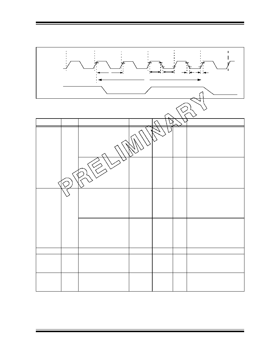
2002 Microchip Technology Inc.
Preliminary
DS41159B-page 337
PIC18FXX8
27.3.3
TIMING DIAGRAMS AND SPECIFICATIONS
FIGURE 27-5:
EXTERNAL CLOCK TIMING
TABLE 27-6:
EXTERNAL CLOCK TIMING REQUIREMENTS
OSC1
CLKO
Q4
Q1
Q2
Q3
Q4
Q1
1
2
3
3
4
4
Param No.
Symbol
Characteristic
Min
Max
Units
Conditions
1A
F
OSC
External CLKI Frequency
(1)
DC
4
MHz
XT osc
DC
25
MHz
HS osc
4
10
MHz
HS + PLL osc
DC
DC
200
40
kHz
MHz
LP osc
EC
Oscillator Frequency
(1)
DC
4
MHz
RC osc
0.1
4
MHz
XT osc
4
25
MHz
HS osc
4
10
MHz
HS + PLL osc
5
200
kHz
LP osc
1
T
OSC
External CLKI Period
(1)
250
--
ns
XT and RC osc
40
--
ns
HS osc
100
--
ns
HS + PLL osc
5
5
--
--
�
s
ns
LP osc
EC
Oscillator Period
(1)
250
--
ns
RC osc
250
10,000
ns
XT osc
100
40
10,000
100
ns
ns
HS osc
HS + PLL osc
5
--
�
s
LP osc
2
T
CY
Instruction Cycle Time
(1)
100
--
ns
T
CY
= 4/F
OSC
3
TosL,
TosH
External Clock in (OSC1)
High or Low Time
30
--
ns
XT osc
2.5
--
ns
LP osc
10
--
�
s
HS osc
4
TosR,
TosF
External Clock in (OSC1)
Rise or Fall Time
-- 20
ns
XT
osc
-- 50
ns
LP
osc
--
7.5
ns
HS osc
Note 1: Instruction cycle period (T
CY
) equals four times the input oscillator time-base period. All specified values are
based on characterization data for that particular oscillator type under standard operating conditions with
the device executing code. Exceeding these specified limits may result in an unstable oscillator operation
and/or higher than expected current consumption. All devices are tested to operate at "Min." values with an
external clock applied to the OSC1/CLKI pin. When an external clock input is used, the "Max." cycle time
limit is "DC" (no clock) for all devices.
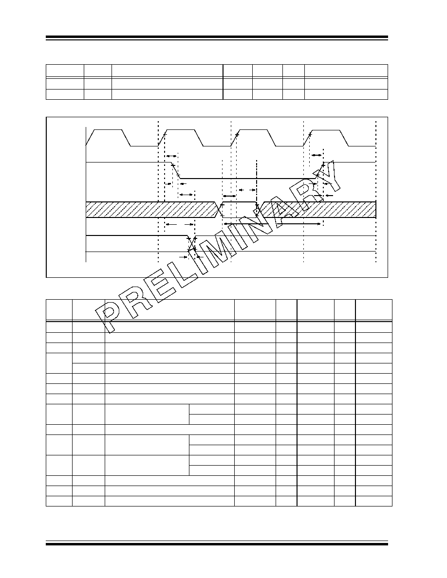
PIC18FXX8
DS41159B-page 338
Preliminary
2002 Microchip Technology Inc.
TABLE 27-7:
PLL CLOCK TIMING SPECIFICATION (V
DD
= 4.2V - 5.5V)
FIGURE 27-6:
CLKO AND I/O TIMING
TABLE 27-8:
CLKO AND I/O TIMING REQUIREMENTS
Param No. Symbol
Characteristic
Min
Max
Units
Conditions
7
T
PLL
PLL Start-up Time (Lock Time)
--
2
ms
CLK
CLKO Stability (Jitter) using PLL
TBD
TBD
%
Param
No.
Symbol
Characteristic
Min
Typ
Max
Units Conditions
10
TosH2ckL OSC1
to CLKO
--
75
200
ns
(1)
11
TosH2ckH OSC1
to CLKO
--
75
200
ns
(1)
12
TckR
CLKO rise time
--
35
100
ns
(1)
13
TckF
CLKO fall time
--
35
100
ns
(1)
14
TckL2ioV CLKO
to Port out valid
--
--
0.5 T
CY
+ 20
ns
(1)
15
TioV2ckH Port in valid before CLKO
0.25
T
CY
+ 25
--
--
ns
(1)
16
TckH2ioI
Port in hold after CLKO
0
--
--
ns
(1)
17
TosH2ioV OSC1
(Q1 cycle) to Port out valid
--
50
150
ns
18
TosH2ioI
OSC1
(Q2 cycle) to Port
input invalid (I/O in hold time)
PIC18FXX8
100
--
--
ns
18A
PIC18LFXX8
200
--
--
ns
19
TioV2osH Port input valid to OSC1
(I/O in setup time)
0
--
--
ns
20
T
IO
R
Port output rise time
PIC18FXX8
--
10
25
ns
20A
PIC18LFXX8
--
--
60
ns
21
T
IO
F
Port output fall time
PIC18FXX8
--
10
25
ns
21A
PIC18LFXX8
--
--
60
ns
22
T
INP
INT pin high or low time
T
CY
--
--
ns
23
T
RBP
RB7:RB4 change INT high or low time
T
CY
--
--
ns
24
T
RCP
RC7:RC4 change INT high or low time
20
--
--
ns
These parameters are asynchronous events, not related to any internal clock edges.
Note 1: Measurements are taken in RC mode where CLKO pin output is 4 x T
OSC
.
Note: Refer to Figure 27-4 for load conditions.
OSC1
CLKO
I/O Pin
(Input)
I/O Pin
(Output)
Q4
Q1
Q2
Q3
10
13
14
17
20, 21
19
18
15
11
12
16
Old Value
New Value
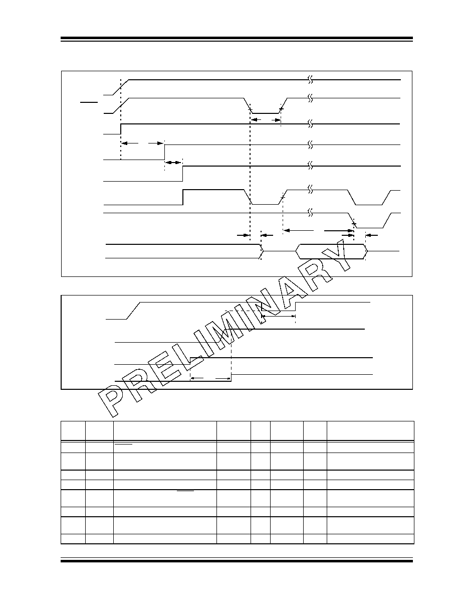
2002 Microchip Technology Inc.
Preliminary
DS41159B-page 339
PIC18FXX8
FIGURE 27-7:
RESET, WATCHDOG TIMER, OSCILLATOR START-UP TIMER AND POWER-UP
TIMER TIMING
FIGURE 27-8:
BROWN-OUT RESET AND LOW VOLTAGE DETECT TIMING
TABLE 27-9:
RESET, WATCHDOG TIMER, OSCILLATOR START-UP TIMER, POWER-UP TIMER,
BROWN-OUT RESET AND LOW VOLTAGE DETECT REQUIREMENTS
Param
No.
Symbol
Characteristic
Min
Typ
Max
Units
Conditions
30
TmcL
MCLR Pulse Width (low)
2
--
--
�
s
31
T
WDT
Watchdog Timer Time-out Period
(No Prescaler)
7
18
33
ms
32
T
OST
Oscillation Start-up Timer Period
1024 T
OSC
--
1024 T
OSC
--
T
OSC
= OSC1 period
33
T
PWRT
Power-up Timer Period
28
72
132
ms
34
T
IOZ
I/O Hi-impedance from MCLR Low or
Watchdog Timer Reset
--
2
--
�
s
35
T
BOR
Brown-out Reset Pulse Width
200
--
--
�
s
For V
DD
BV
DD
(see D005)
36
T
IVRST
Time for Internal Reference
Voltage to become stable
--
20
50
�
s
37
T
LVD
Low Voltage Detect Pulse Width
200
--
--
�
s
For V
DD
V
LVD
(see D420)
V
DD
MCLR
Internal
POR
PWRT
Time-out
OSC
Time-out
Internal
Reset
Watchdog
Timer
Reset
33
32
30
31
34
I/O Pins
34
Note: Refer to Figure 27-4 for load conditions.
V
DD
BV
DD
(for 35)
35, 37
V
BGAP
= 1.2V
V
IRVS
T
Enable Internal Reference Voltage
Internal Reference Voltage stable
36
V
LVD
(for 37)
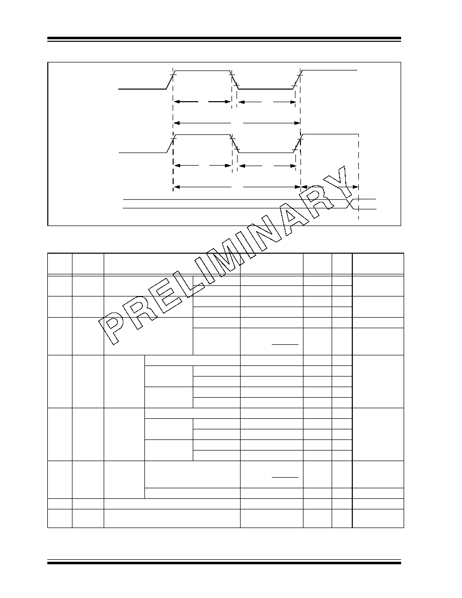
PIC18FXX8
DS41159B-page 340
Preliminary
2002 Microchip Technology Inc.
FIGURE 27-9:
TIMER0 AND TIMER1 EXTERNAL CLOCK TIMINGS
TABLE 27-10: TIMER0 AND TIMER1 EXTERNAL CLOCK REQUIREMENTS
Param
No.
Symbol
Characteristic
Min
Max
Units
Conditions
40
Tt0H
T0CKI High Pulse Width
No prescaler
0.5 T
CY
+ 20
--
ns
With prescaler
10
--
ns
41
Tt0L
T0CKI Low Pulse Width
No prescaler
0.5 T
CY
+ 20
--
ns
With prescaler
10
--
ns
42
Tt0P
T0CKI Period
No prescaler
T
CY
+ 10
--
ns
With prescaler
Greater of:
20 ns or T
CY
+ 40
N
--
ns
N = prescale
value
(1, 2, 4,..., 256)
45
Tt1H
T1CKI
High Time
Synchronous, no prescaler
0.5 T
CY
+ 20
--
ns
Synchronous,
with prescaler
PIC18FXX8
10
--
ns
PIC18LFXX8
25
--
ns
Asynchronous PIC18FXX8
30
--
ns
PIC18LFXX8
50
--
ns
46
Tt1L
T1CKI
Low Time
Synchronous, no prescaler
0.5 T
CY
+ 5
--
ns
Synchronous,
with prescaler
PIC18FXX8
10
--
ns
PIC18LFXX8
25
--
ns
Asynchronous PIC18FXX8
30
--
ns
PIC18LFXX8
TBD
TBD
ns
47
Tt1P
T1CKI
Input Period
Synchronous
Greater of:
20 ns or T
CY
+ 40
N
--
ns
N = prescale
value
(1, 2, 4, 8)
Asynchronous
60
--
ns
Ft1
T1CKI Oscillator Input Frequency Range
DC
50
kHz
48
Tcke2tmrI Delay from External T1CKI Clock Edge to
Timer Increment
2 T
OSC
7 T
OSC
--
Note: Refer to Figure 27-4 for load conditions.
46
47
45
48
41
42
40
T0CKI
T1OSO/T1CKI
TMR0 o
r
TMR1
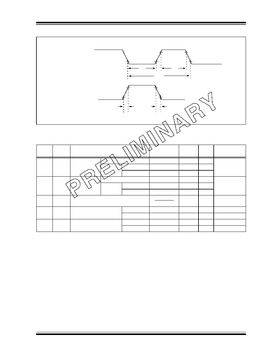
2002 Microchip Technology Inc.
Preliminary
DS41159B-page 341
PIC18FXX8
FIGURE 27-10:
CAPTURE/COMPARE/PWM TIMINGS (CCP1 AND ECCP1)
TABLE 27-11: CAPTURE/COMPARE/PWM REQUIREMENTS (CCP1 AND ECCP1)
Note: Refer to Figure 27-4 for load conditions.
CCPx
(Capture Mode)
50
51
52
CCPx
53
54
(Compare or PWM Mode)
Param
No.
Symbol
Characteristic
Min
Max
Units
Conditions
50
TccL
CCPx input low
time
No Prescaler
0.5 T
CY
+ 20
--
ns
With
Prescaler
PIC18FXX8
10
--
ns
PIC18LFXX8
20
--
ns
51
TccH
CCPx input
high time
No Prescaler
0.5 T
CY
+ 20
--
ns
With
Prescaler
PIC18FXX8
10
--
ns
PIC18LFXX8
20
--
ns
52
TccP
CCPx input period
3 T
CY
+ 40
N
--
ns
N = prescale
value (1,4 or 16)
53
TccR
CCPx output fall time
PIC18FXX8
--
25
ns
PIC18LFXX8
--
45
ns
54
TccF
CCPx output fall time
PIC18FXX8
--
25
ns
PIC18LFXX8
--
45
ns
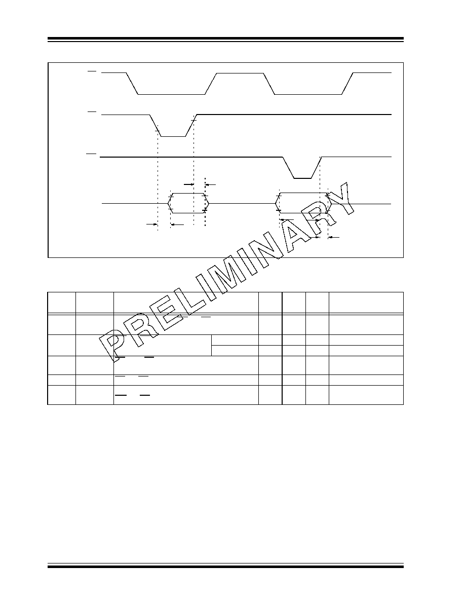
PIC18FXX8
DS41159B-page 342
Preliminary
2002 Microchip Technology Inc.
FIGURE 27-11:
PARALLEL SLAVE PORT TIMING (PIC18F248 AND PIC18F458)
TABLE 27-12: PARALLEL SLAVE PORT REQUIREMENTS (PIC18F248 AND PIC18F458)
Note: Refer to Figure 27-4 for load conditions.
RE2/CS
RE0/RD
RE1/WR
RD7:RD0
62
63
64
65
Param
No.
Symbol
Characteristic
Min
Max
Units
Conditions
62
TdtV2wrH
Data-in valid before WR
or CS
(setup time)
20
25
--
--
ns
ns
Extended Temp. range
63
TwrH2dtI
WR
or CS
to data-in invalid
(hold time)
PIC18FXX8
20
--
ns
PIC18LFXX8
35
--
ns
64
TrdL2dtV
RD
and CS
to data-out valid
--
--
80
90
ns
ns
Extended Temp. range
65
TrdH2dtI
RD
or CS
to data-out invalid
10
30
ns
66
TibfINH
Inhibit the IBF flag bit being cleared from
WR
or CS
--
3 T
CY
ns
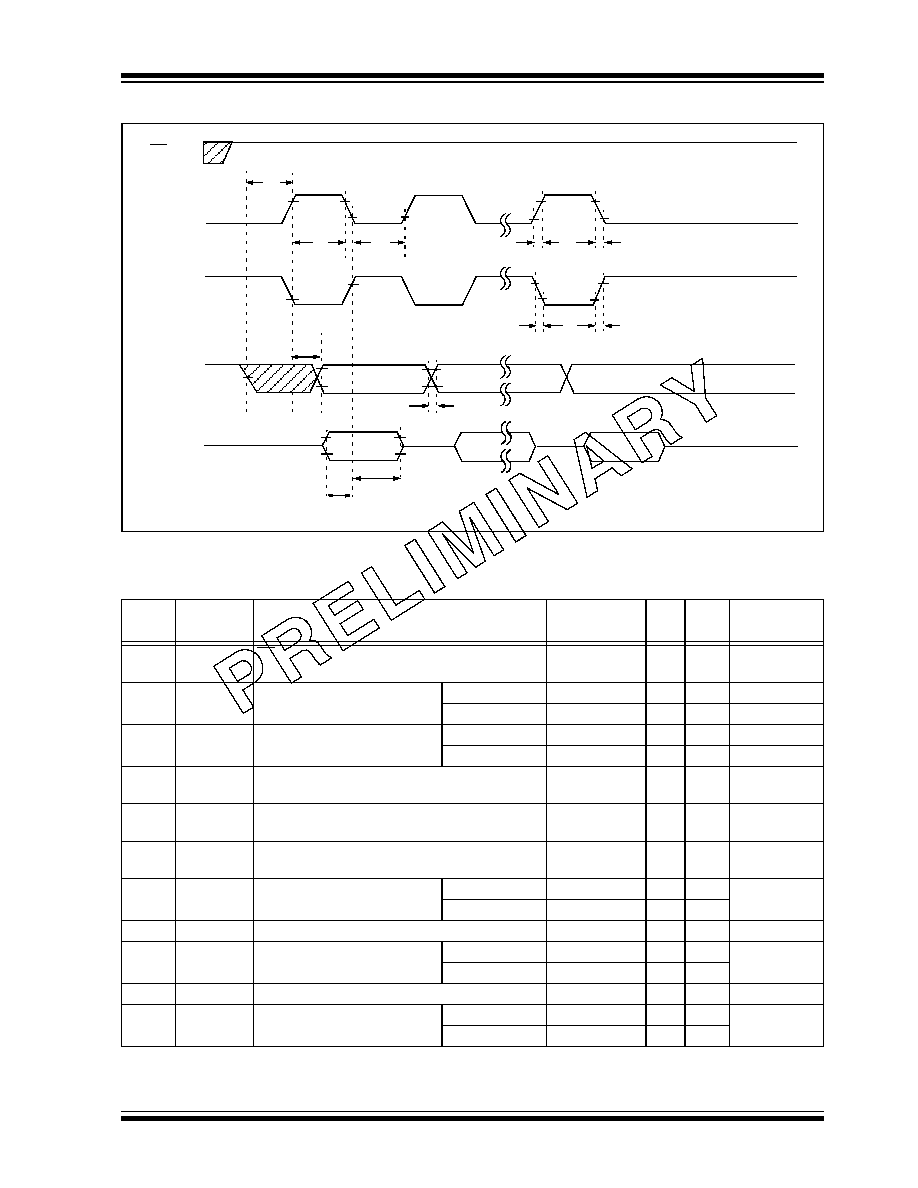
2002 Microchip Technology Inc.
Preliminary
DS41159B-page 343
PIC18FXX8
FIGURE 27-12:
EXAMPLE SPI MASTER MODE TIMING (CKE = 0)
TABLE 27-13: EXAMPLE SPI MODE REQUIREMENTS (MASTER MODE, CKE = 0)
SS
SCK
(CKP = 0)
SCK
(CKP = 1)
SDO
SDI
70
71
72
73
74
75, 76
78
79
80
79
78
MSb
LSb
Bit6 - - - - - -1
MSb In
LSb In
Bit6 - - - -1
Note: Refer to Figure 27-4 for load conditions.
Param
No.
Symbol
Characteristic
Min
Max Units
Conditions
70
TssL2scH,
TssL2scL
SS
to SCK
or SCK
input
T
CY
--
ns
71
TscH
SCK input high time
(Slave mode)
Continuous
1.25 T
CY
+ 30
--
ns
71A
Single Byte
40
--
ns
(Note 1)
72
TscL
SCK input low time
(Slave mode)
Continuous
1.25 T
CY
+ 30
--
ns
72A
Single Byte
40
--
ns
(Note 1)
73
TdiV2scH,
TdiV2scL
Setup time of SDI data input to SCK edge
100
--
ns
73A
T
B
2
B
Last clock edge of Byte1 to the 1st clock edge of
Byte2
1.5 T
CY
+ 40
--
ns
(Note 2)
74
TscH2diL,
TscL2diL
Hold time of SDI data input to SCK edge
100
--
ns
75
TdoR
SDO data output rise time
PIC18FXX8
--
25
ns
PIC18LFXX8
--
45
ns
76
TdoF
SDO data output fall time
--
25
ns
78
TscR
SCK output rise time
(Master mode)
PIC18FXX8
--
25
ns
PIC18LFXX8
--
45
ns
79
TscF
SCK output fall time (Master mode)
--
25
ns
80
TscH2doV,
TscL2doV
SDO data output valid after
SCK edge
PIC18FXX8
--
50
ns
PIC18LFXX8
--
100
ns
Note 1: Requires the use of parameter # 73A.
2: Only if parameter #'s 71A and 72A are used.
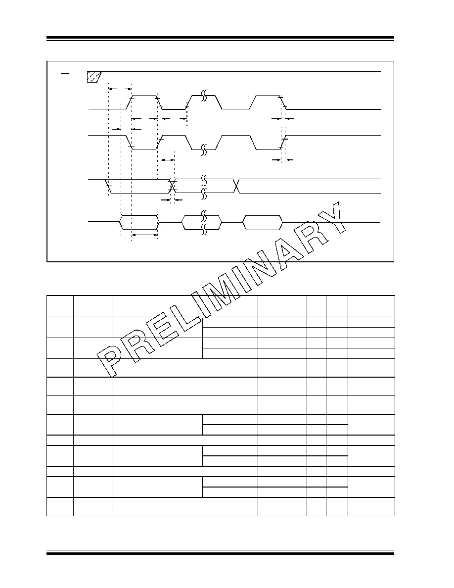
PIC18FXX8
DS41159B-page 344
Preliminary
2002 Microchip Technology Inc.
FIGURE 27-13:
EXAMPLE SPI MASTER MODE TIMING (CKE = 1)
TABLE 27-14: EXAMPLE SPI MODE REQUIREMENTS (MASTER MODE, CKE = 1)
SS
SCK
(CKP = 0)
SCK
(CKP = 1)
SDO
SDI
81
71
72
74
75, 76
78
80
MSb
79
73
MSb In
Bit6 - - - - - -1
LSb In
Bit6 - - - -1
LSb
Note: Refer to Figure 27-4 for load conditions.
Param
No.
Symbol
Characteristic
Min
Max Units
Conditions
71
TscH
SCK input high time
(Slave mode)
Continuous
1.25 T
CY
+ 30
--
ns
71A
Single Byte
40
--
ns
(Note 1)
72
TscL
SCK input low time
(Slave mode)
Continuous
1.25 T
CY
+ 30
--
ns
72A
Single Byte
40
--
ns
(Note 1)
73
TdiV2scH,
TdiV2scL
Setup time of SDI data input to SCK edge
100
--
ns
73A
T
B
2
B
Last clock edge of Byte1 to the 1st clock edge of
Byte2
1.5 T
CY
+ 40
--
ns
(Note 2)
74
TscH2diL,
TscL2diL
Hold time of SDI data input to SCK edge
100
--
ns
75
TdoR
SDO data output rise time
PIC18FXX8
--
25
ns
PIC18LFXX8
--
45
ns
76
TdoF
SDO data output fall time
--
25
ns
78
TscR
SCK output rise time
(Master mode)
PIC18FXX8
--
25
ns
PIC18LFXX8
--
45
ns
79
TscF
SCK output fall time (Master mode)
--
25
ns
80
TscH2doV,
TscL2doV
SDO data output valid after
SCK edge
PIC18FXX8
--
50
ns
PIC18LFXX8
--
100
ns
81
TdoV2scH,
TdoV2scL
SDO data output setup to SCK edge
T
CY
--
ns
Note 1: Requires the use of parameter # 73A.
2: Only if parameter #'s 71A and 72A are used.
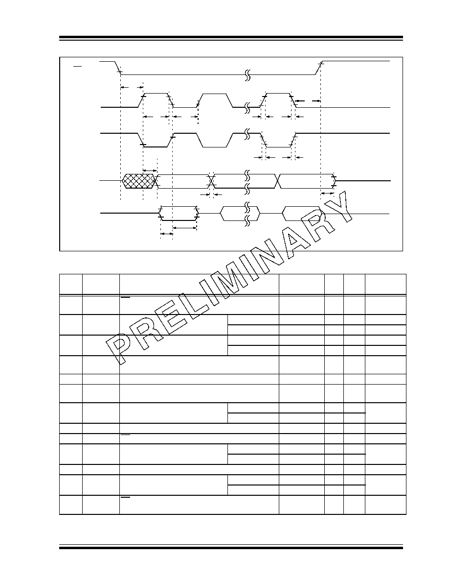
2002 Microchip Technology Inc.
Preliminary
DS41159B-page 345
PIC18FXX8
FIGURE 27-14:
EXAMPLE SPI SLAVE MODE TIMING (CKE = 0)
SS
SCK
(CKP = 0)
SCK
(CKP = 1)
SDO
SDI
70
71
72
73
74
75, 76
77
78
79
80
79
78
MSb
LSb
Bit6 - - - - - -1
MSb In
Bit6 - - - -1
LSb In
83
Note: Refer to Figure 27-4 for load conditions.
TABLE 27-15: EXAMPLE SPI MODE REQUIREMENTS, SLAVE MODE TIMING (CKE = 0)
Param
No.
Symbol
Characteristic
Min
Max Units Conditions
70
TssL2scH,
TssL2scL
SS
to SCK
or SCK
input
T
CY
--
ns
71
TscH
SCK input high time (Slave mode)
Continuous
1.25 T
CY
+ 30
--
ns
71A
Single Byte
40
--
ns
(Note 1)
72
TscL
SCK input low time (Slave mode)
Continuous
1.25 T
CY
+ 30
--
ns
72A
Single Byte
40
--
ns
(Note 1)
73
TdiV2scH,
TdiV2scL
Setup time of SDI data input to SCK edge
100
--
ns
73A
T
B
2
B
Last clock edge of Byte1 to the 1st clock edge of Byte2
1.5 T
CY
+ 40
--
ns
(Note 2)
74
TscH2diL,
TscL2diL
Hold time of SDI data input to SCK edge
100
--
ns
75
TdoR
SDO data output rise time
PIC18FXX8
--
25
ns
PIC18LFXX8
45
ns
76
TdoF
SDO data output fall time
--
25
ns
77
TssH2doZ
SS
to SDO output hi-impedance
10
50
ns
78
TscR
SCK output rise time (Master mode) PIC18FXX8
--
25
ns
PIC18LFXX8
45
ns
79
TscF
SCK output fall time (Master mode)
--
25
ns
80
TscH2doV,
TscL2doV
SDO data output valid after SCK
edge
PIC18FXX8
--
50
ns
PIC18LFXX8
100
ns
83
TscH2ssH,
TscL2ssH
SS
after SCK edge
1.5 T
CY
+ 40
--
ns
Note 1: Requires the use of parameter # 73A.
2: Only if parameter #'s 71A and 72A are used.
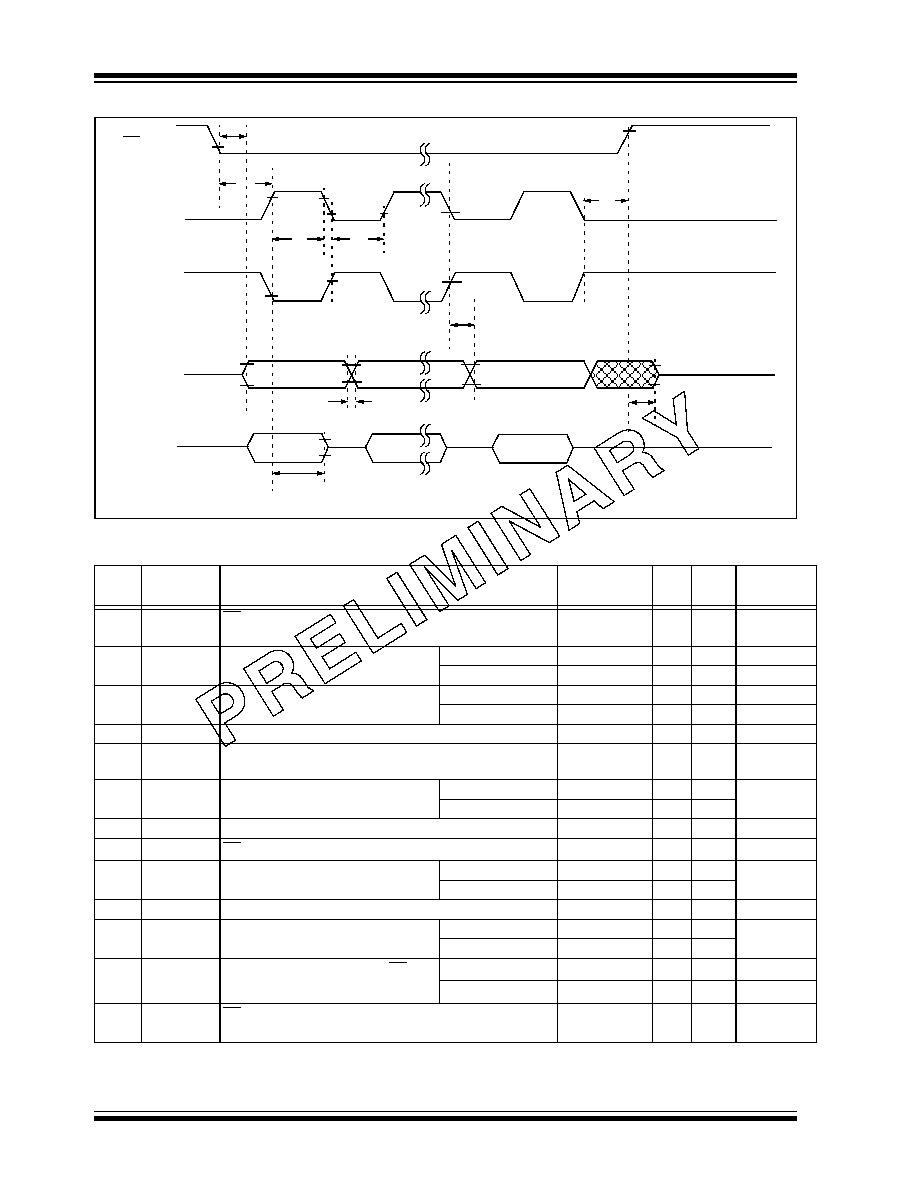
PIC18FXX8
DS41159B-page 346
Preliminary
2002 Microchip Technology Inc.
FIGURE 27-15:
EXAMPLE SPI SLAVE MODE TIMING (CKE = 1)
SS
SCK
(CKP = 0)
SCK
(CKP = 1)
SDO
SDI
70
71
72
82
74
75, 76
MSb
Bit6 - - - - - -1
LSb
77
MSb In
Bit6 - - - -1
LSb In
80
83
Note: Refer to Figure 27-4 for load conditions.
TABLE 27-16: EXAMPLE SPI SLAVE MODE REQUIREMENTS (CKE = 1)
Param
No.
Symbol
Characteristic
Min
Max Units Conditions
70
TssL2scH,
TssL2scL
SS
to SCK
or SCK
input
T
CY
--
ns
71
TscH
SCK input high time
(Slave mode)
Continuous
1.25 T
CY
+ 30
--
ns
71A
Single Byte
40
--
ns
(Note 1)
72
TscL
SCK input low time
(Slave mode)
Continuous
1.25 T
CY
+ 30
--
ns
72A
Single Byte
40
--
ns
(Note 1)
73A
T
B
2
B
Last clock edge of Byte1 to the 1st clock edge of Byte2
1.5 T
CY
+ 40
--
ns
(Note 2)
74
TscH2diL,
TscL2diL
Hold time of SDI data input to SCK edge
100
--
ns
75
TdoR
SDO data output rise time
PIC18FXX8
--
25
ns
PIC18LFXX8
--
45
ns
76
TdoF
SDO data output fall time
--
25
ns
77
TssH2doZ
SS
to SDO output hi-impedance
10
50
ns
78
TscR
SCK output rise time
(Master mode)
PIC18FXX8
--
25
ns
PIC18LFXX8
--
45
ns
79
TscF
SCK output fall time (Master mode)
--
25
ns
80
TscH2doV,
TscL2doV
SDO data output valid after SCK
edge
PIC18FXX8
--
50
ns
PIC18LFXX8
--
100
ns
82
TssL2doV
SDO data output valid after SS
edge
PIC18FXX8
--
50
ns
PIC18LFXX8
--
100
ns
83
TscH2ssH,
TscL2ssH
SS
after SCK edge
1.5 T
CY
+ 40
--
ns
Note 1: Requires the use of parameter # 73A.
2: Only if parameter #'s 71A and 72A are used.
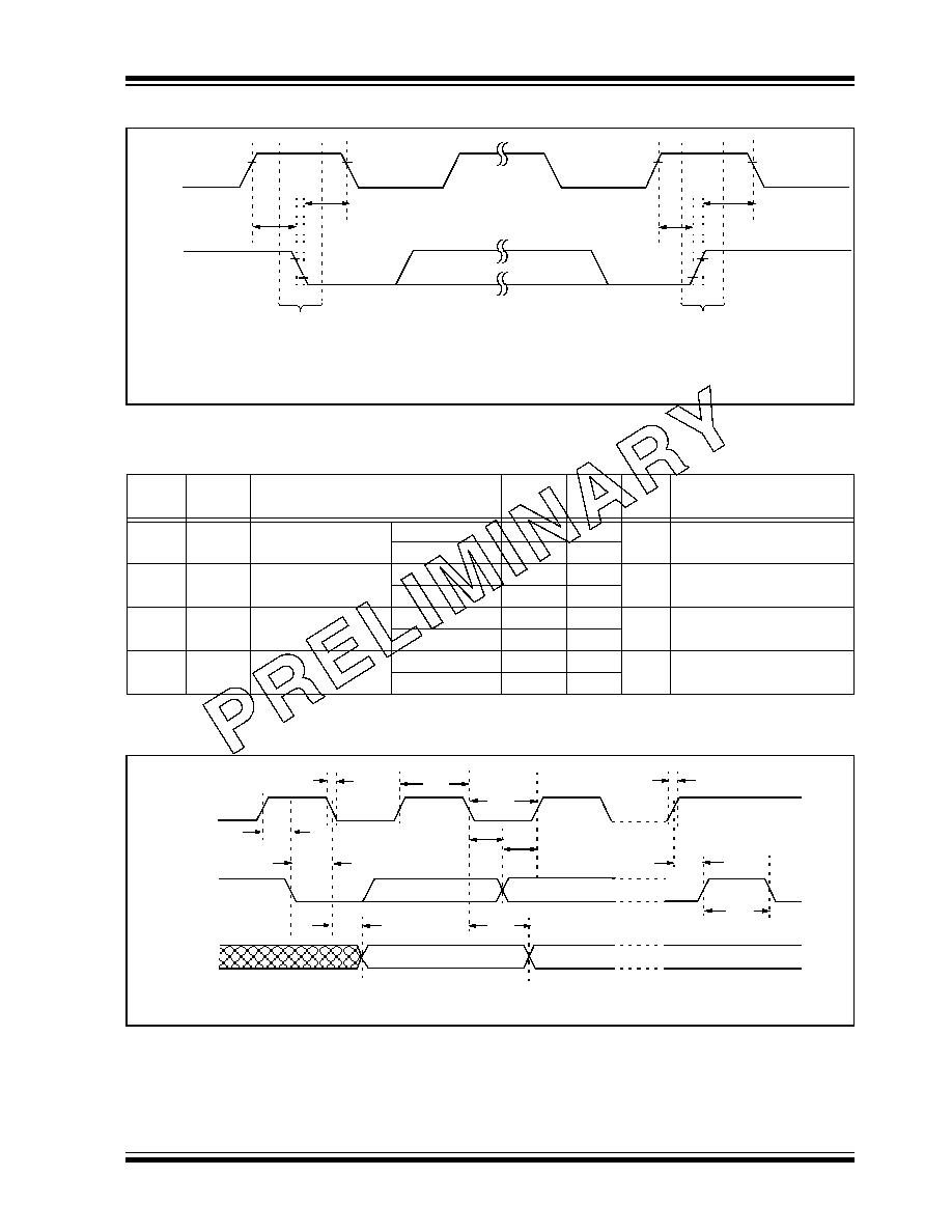
2002 Microchip Technology Inc.
Preliminary
DS41159B-page 347
PIC18FXX8
FIGURE 27-16:
I
2
C BUS START/STOP BITS TIMING
TABLE 27-17: I
2
C BUS START/STOP BITS REQUIREMENTS (SLAVE MODE)
FIGURE 27-17:
I
2
C BUS DATA TIMING
Note: Refer to Figure 27-4 for load conditions.
91
92
93
SCL
SDA
START
Condition
STOP
Condition
90
Param
No.
Symbol
Characteristic
Min
Max
Units
Conditions
90
T
SU
:
STA
START condition
100 kHz mode
4700
--
ns
Only relevant for Repeated
START condition
Setup time
400 kHz mode
600
--
91
T
HD
:
STA
START condition
100 kHz mode
4000
--
ns
After this period, the first
clock pulse is generated
Hold time
400 kHz mode
600
--
92
T
SU
:
STO
STOP condition
100 kHz mode
4700
--
ns
Setup time
400 kHz mode
600
--
93
T
HD
:
STO
STOP condition
100 kHz mode
4000
--
ns
Hold time
400 kHz mode
600
--
Note: Refer to Figure 27-4 for load conditions.
90
91
92
100
101
103
106
107
109
109
110
102
SCL
SDA
In
SDA
Out

PIC18FXX8
DS41159B-page 348
Preliminary
2002 Microchip Technology Inc.
TABLE 27-18: I
2
C BUS DATA REQUIREMENTS (SLAVE MODE)
Param
No.
Symbol
Characteristic
Min
Max
Units
Conditions
100
T
HIGH
Clock high time
100 kHz mode
4.0
--
�
s
PIC18FXX8 must operate
at a minimum of 1.5 MHz
400 kHz mode
0.6
--
�
s
PIC18FXX8 must operate
at a minimum of 10 MHz
SSP Module
1.5 T
CY
--
101
T
LOW
Clock low time
100 kHz mode
4.7
--
�
s
PIC18FXX8 must operate
at a minimum of 1.5 MHz
400 kHz mode
1.3
--
�
s
PIC18FXX8 must operate
at a minimum of 10 MHz
SSP module
1.5 T
CY
--
ns
102
T
R
SDA and SCL rise
time
100 kHz mode
--
1000
ns
400 kHz mode
20 + 0.1 C
B
300
ns
C
B
is specified to be from
10 to 400 pF
103
T
F
SDA and SCL fall
time
100 kHz mode
--
300
ns
400 kHz mode
20 + 0.1 C
B
300
ns
C
B
is specified to be from
10 to 400 pF
90
T
SU
:
STA
START condition
setup time
100 kHz mode
4.7
--
�
s
Only relevant for Repeated
START condition
400 kHz mode
0.6
--
�
s
91
T
HD
:
STA
START condition
hold time
100 kHz mode
4.0
--
�
s
After this period the first
clock pulse is generated
400 kHz mode
0.6
--
�
s
106
T
HD
:
DAT
Data input hold
time
100 kHz mode
0
--
ns
400 kHz mode
0
0.9
�
s
107
T
SU
:
DAT
Data input setup
time
100 kHz mode
250
--
ns
(Note 2)
400 kHz mode
100
--
ns
92
T
SU
:
STO
STOP condition
setup time
100 kHz mode
4.7
--
�
s
400 kHz mode
0.6
--
�
s
109
T
AA
Output valid from
clock
100 kHz mode
--
3500
ns
(Note 1)
400 kHz mode
--
--
ns
110
T
BUF
Bus free time
100 kHz mode
4.7
--
�
s
Time the bus must be free
before a new transmission
can start
400 kHz mode
1.3
--
�
s
D102
C
B
Bus capacitive loading
--
400
pF
Note 1: As a transmitter, the device must provide this internal minimum delay time to bridge the undefined region
(min. 300 ns) of the falling edge of SCL to avoid unintended generation of START or STOP conditions.
2: A Fast mode I
2
C bus device can be used in a Standard mode I
2
C bus system, but the requirement
T
SU
;
DAT
250 ns must then be met. This will automatically be the case if the device does not stretch the
LOW period of the SCL signal. If such a device does stretch the LOW period of the SCL signal, it must
output the next data bit to the SDA line.
Before the SCL line is released, T
R
max. + T
SU
;
DAT
= 1000 + 250 = 1250 ns (according to the Standard
mode I
2
C bus specification).
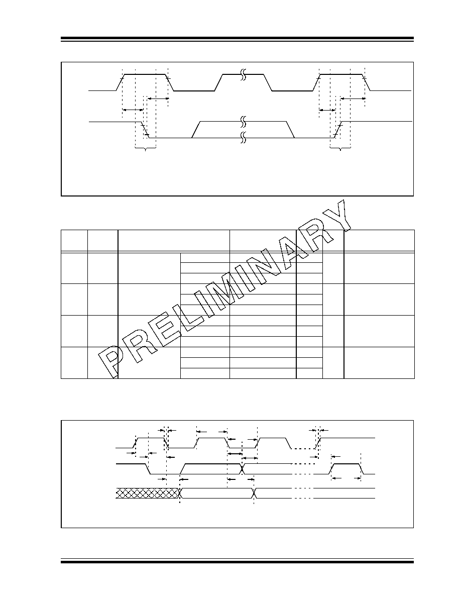
2002 Microchip Technology Inc.
Preliminary
DS41159B-page 349
PIC18FXX8
FIGURE 27-18:
MASTER SSP I
2
C BUS START/STOP BITS TIMING WAVEFORMS
TABLE 27-19: MASTER SSP I
2
C BUS START/STOP BITS REQUIREMENTS
FIGURE 27-19:
MASTER SSP I
2
C BUS DATA TIMING
Note: Refer to Figure 27-4 for load conditions.
91
93
SCL
SDA
START
Condition
STOP
Condition
90
92
Param
No.
Symbol
Characteristic
Min
Max
Units
Conditions
90
T
SU
:
STA
START condition
100 kHz mode
2(T
OSC
)(BRG + 1)
--
ns
Only relevant for
Repeated START
condition
Setup time
400 kHz mode
2(T
OSC
)(BRG + 1)
--
1 MHz mode
(1)
2(T
OSC
)(BRG + 1)
--
91
T
HD
:
STA
START condition
100 kHz mode
2(T
OSC
)(BRG + 1)
--
ns
After this period, the
first clock pulse is
generated
Hold time
400 kHz mode
2(T
OSC
)(BRG + 1)
--
1 MHz mode
(1)
2(T
OSC
)(BRG + 1)
--
92
T
SU
:
STO
STOP condition
100 kHz mode
2(T
OSC
)(BRG + 1)
--
ns
Setup time
400 kHz mode
2(T
OSC
)(BRG + 1)
--
1 MHz mode
(1)
2(T
OSC
)(BRG + 1)
--
93
T
HD
:
STO
STOP condition
100 kHz mode
2(T
OSC
)(BRG + 1)
--
ns
Hold time
400 kHz mode
2(T
OSC
)(BRG + 1)
--
1 MHz mode
(1)
2(T
OSC
)(BRG + 1)
--
Note 1: Maximum pin capacitance = 10 pF for all I
2
C pins.
Note: Refer to Figure 27-4 for load conditions.
90
91
92
100
101
103
106
107
109
109
110
102
SCL
SDA
In
SDA
Out

PIC18FXX8
DS41159B-page 350
Preliminary
2002 Microchip Technology Inc.
TABLE 27-20: MASTER SSP I
2
C BUS DATA REQUIREMENTS
Param.
No.
Symbol
Characteristic
Min
Max
Units
Conditions
100
T
HIGH
Clock high time 100 kHz mode
2(T
OSC
)(BRG + 1)
--
ms
400 kHz mode
2(T
OSC
)(BRG + 1)
--
ms
1 MHz mode
(1)
2(T
OSC
)(BRG + 1)
--
ms
101
T
LOW
Clock low time
100 kHz mode
2(T
OSC
)(BRG + 1)
--
ms
400 kHz mode
2(T
OSC
)(BRG + 1)
--
ms
1 MHz mode
(1)
2(T
OSC
)(BRG + 1)
--
ms
102
T
R
SDA and SCL
rise time
100 kHz mode
--
1000
ns
C
B
is specified to be from
10 to 400 pF
400 kHz mode
20 + 0.1 C
B
300
ns
1 MHz mode
(1)
--
300
ns
103
T
F
SDA and SCL
fall time
100 kHz mode
--
300
ns
C
B
is specified to be from
10 to 400 pF
400 kHz mode
20 + 0.1 C
B
300
ns
1 MHz mode
(1)
--
100
ns
90
T
SU
:
STA
START condition
setup time
100 kHz mode
2(T
OSC
)(BRG + 1)
--
ms
Only relevant for
Repeated START
condition
400 kHz mode
2(T
OSC
)(BRG + 1)
--
ms
1 MHz mode
(1)
2(T
OSC
)(BRG + 1)
--
ms
91
T
HD
:
STA
START condition
hold time
100 kHz mode
2(T
OSC
)(BRG + 1)
--
ms
After this period, the first
clock pulse is generated
400 kHz mode
2(T
OSC
)(BRG + 1)
--
ms
1 MHz mode
(1)
2(T
OSC
)(BRG + 1)
--
ms
106
T
HD
:
DAT
Data input
hold time
100 kHz mode
0
--
ns
400 kHz mode
0
0.9
ms
1 MHz mode
(1)
TBD
--
ns
107
T
SU
:
DAT
Data input
setup time
100 kHz mode
250
--
ns
(Note 2)
400 kHz mode
100
--
ns
1 MHz mode
(1)
TBD
--
ns
92
T
SU
:
STO
STOP condition
setup time
100 kHz mode
2(T
OSC
)(BRG + 1)
--
ms
400 kHz mode
2(T
OSC
)(BRG + 1)
--
ms
1 MHz mode
(1)
2(T
OSC
)(BRG + 1)
--
ms
109
T
AA
Output valid from
clock
100 kHz mode
--
3500
ns
400 kHz mode
--
1000
ns
1 MHz mode
(1)
--
--
ns
110
T
BUF
Bus free time
100 kHz mode
4.7
--
ms
Time the bus must be free
before a new transmission
can start
400 kHz mode
1.3
--
ms
1 MHz mode
(1)
TBD
--
ms
D102
C
B
Bus capacitive loading
--
400
pF
Note 1: Maximum pin capacitance = 10 pF for all I
2
C pins.
2: A Fast mode I
2
C bus device can be used in a Standard mode I
2
C bus system, but parameter #107
250 ns
must then be met. This will automatically be the case if the device does not stretch the LOW period of the SCL
signal. If such a device does stretch the LOW period of the SCL signal, it must output the next data bit to the
SDA line. Before the SCL line is released, parameter #102 + parameter #107 = 1000 + 250 = 1250 ns (for
100 kHz mode).
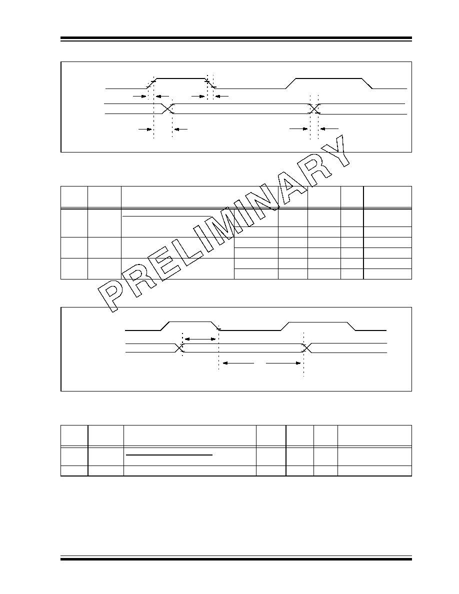
2002 Microchip Technology Inc.
Preliminary
DS41159B-page 351
PIC18FXX8
FIGURE 27-20:
USART SYNCHRONOUS TRANSMISSION (MASTER/SLAVE) TIMING
TABLE 27-21: USART SYNCHRONOUS TRANSMISSION REQUIREMENTS
FIGURE 27-21:
USART SYNCHRONOUS RECEIVE (MASTER/SLAVE) TIMING
TABLE 27-22: USART SYNCHRONOUS RECEIVE REQUIREMENTS
Note: Refer to Figure 27-4 for load conditions.
121
121
120
122
RC6/TX/CK
RC7/RX/DT
pin
pin
Param
No.
Symbol
Characteristic
Min
Max
Units
Conditions
120
TckH2dtV SYNC XMIT (Master & Slave)
Clock high to data-out valid
PIC18FXX8
--
40
ns
PIC18LFXX8
--
100
ns
121
Tckrf
Clock out rise time and fall time
(Master mode)
PIC18FXX8
--
20
ns
PIC18LFXX8
--
50
ns
122
Tdtrf
Data-out rise time and fall time
PIC18FXX8
--
20
ns
PIC18LFXX8
--
50
ns
Note: Refer to Figure 27-4 for load conditions.
125
126
RC6/TX/CK
RC7/RX/DT
pin
pin
Param
No.
Symbol
Characteristic
Min
Max
Units
Conditions
125
TdtV2ckl
SYNC RCV (Master & Slave)
Data-hold before CK
(DT hold time)
10
--
ns
126
TckL2dtl
Data-hold after CK
(DT hold time)
15
--
ns

PIC18FXX8
DS41159B-page 352
Preliminary
2002 Microchip Technology Inc.
TABLE 27-23: A/D CONVERTER CHARACTERISTICS: PIC18FXX8 (INDUSTRIAL, EXTENDED)
PIC18LFXX8 (INDUSTRIAL)
Param
No.
Symbol
Characteristic
Min
Typ
Max
Units
Conditions
A01
N
R
Resolution
--
--
--
--
10
TBD
bit
bit
V
REF
= V
DD
3.0V
V
REF
= V
DD
<
3.0V
A03
E
IL
Integral linearity error
--
--
--
--
<�1
TBD
LSb
LSb
V
REF
= V
DD
3.0V
V
REF
= V
DD
<
3.0V
A04
E
DL
Differential linearity error
--
--
--
--
<�1
TBD
LSb
LSb
V
REF
= V
DD
3.0V
V
REF
= V
DD
<
3.0V
A05
E
FS
Full scale error
--
--
--
--
<�1
TBD
LSb
LSb
V
REF
= V
DD
3.0V
V
REF
= V
DD
<
3.0V
A06
E
OFF
Offset error
--
--
--
--
<�1.5
TBD
LSb
LSb
V
REF
= V
DD
3.0V
V
REF
= V
DD
<
3.0V
A10
--
Monotonicity
guaranteed
(3)
--
V
SS
V
AIN
V
REF
A20
V
REF
Reference voltage
(V
REFH
� V
REFL
)
0V
--
--
V
A20A
3V
--
--
V
For 10-bit resolution
A21
V
REFH
Reference voltage High
V
SS
--
V
DD
+ 0.3V
V
A22
V
REFL
Reference voltage Low
V
SS
- 0.3V
--
V
DD
V
A25
V
AIN
Analog input voltage
V
SS
- 0.3V
--
V
REF
+ 0.3V
V
A30
Z
AIN
Recommended impedance of
analog voltage source
--
--
10.0
k
A40
I
AD
A/D conversion
current (V
DD
)
PIC18FXX8
--
180
--
�
A
Average current
consumption when
A/D is on (Note 1).
PIC18LFXX8
--
90
--
�
A
A50
I
REF
V
REF
input current (Note 2)
10
--
--
--
1000
10
�
A
�
A
During V
AIN
acquisition.
Based on differential of
V
HOLD
to V
AIN
. To charge
C
HOLD
.
During A/D conversion
cycle.
Note 1: When A/D is off, it will not consume any current other than minor leakage current. The power-down current
spec includes any such leakage from the A/D module.
V
REF
current is from RA2/AN2/V
REF
- and RA3/AN3/V
REF
+ pins or V
DD
and V
SS
pins, whichever is selected
as reference input.
2: V
SS
V
AIN
V
REF
3: The A/D conversion result never decreases with an increase in the input voltage, and has no missing codes.
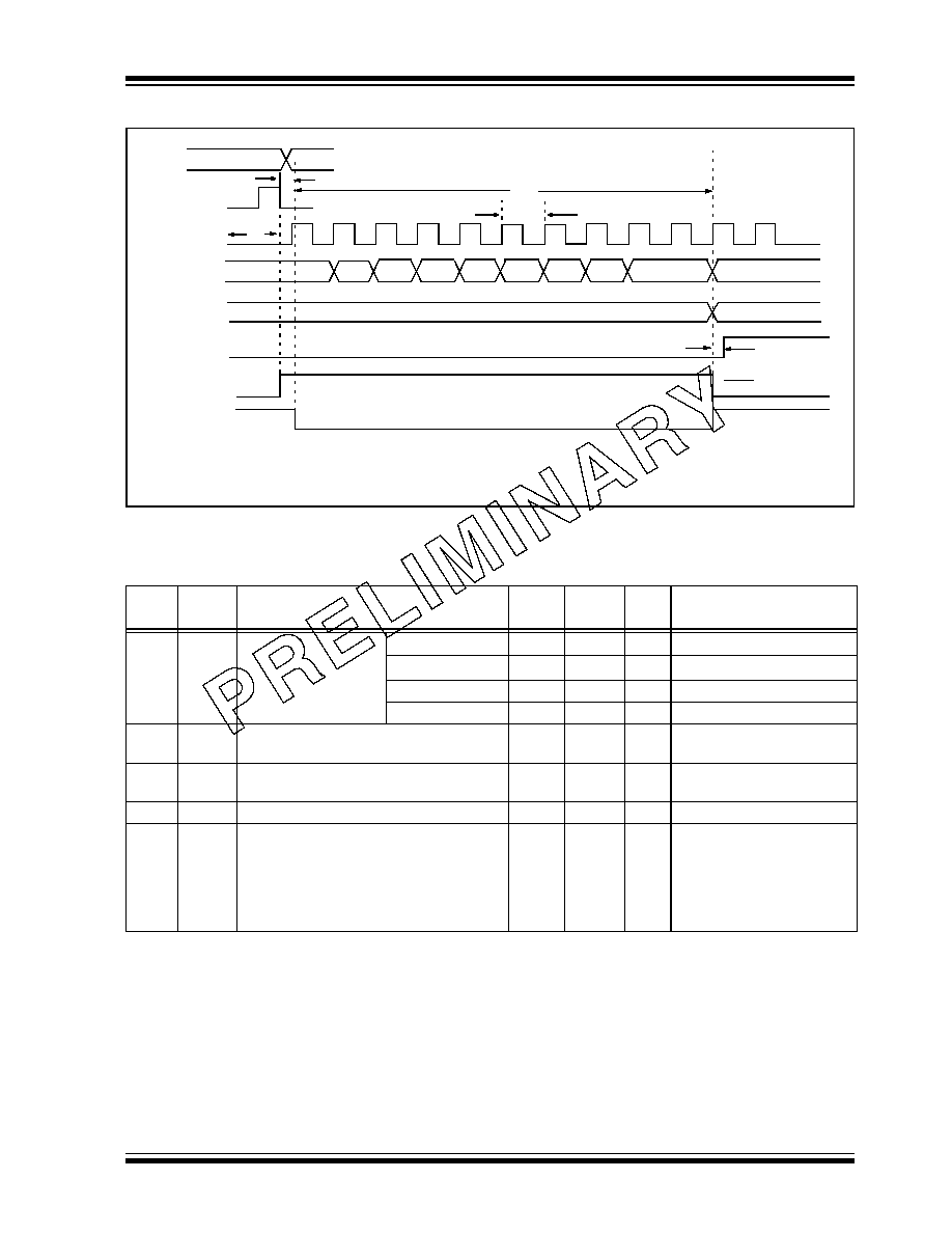
2002 Microchip Technology Inc.
Preliminary
DS41159B-page 353
PIC18FXX8
FIGURE 27-22:
A/D CONVERSION TIMING
TABLE 27-24: A/D CONVERSION REQUIREMENTS
Param
No.
Symbol
Characteristic
Min
Max
Units
Conditions
130
T
AD
A/D clock period
PIC18FXX8
1.6
20
(5)
�
s
T
OSC
based, V
REF
3.0V
PIC18LFXX8
3.0
20
(5)
�
s
T
OSC
based, V
REF
full range
PIC18FXX8
2.0
6.0
�
s
A/D RC mode
PIC18LFXX8
3.0
9.0
�
s
A/D RC mode
131
T
CNV
Conversion time
(not including acquisition time) (Note 1)
11
12
T
AD
132
T
ACQ
Acquisition time (Note 3)
15
10
--
--
�
s
�
s
-40
�
C
Temp
+125
�
C
0
�
C
Temp
+125
�
C
135
T
SWC
Switching time from convert
sample
--
(Note 4)
136
T
AMP
Amplifier settling time (Note 2)
1
--
�
s
This may be used if the
"new" input voltage has not
changed by more than 1 LSb
(i.e., 5 mV @ 5.12V) from the
last sampled voltage (as
stated on C
HOLD
).
Note 1: ADRES register may be read on the following T
CY
cycle.
2: See Section 20.0 for minimum conditions when input voltage has changed more than 1 LSb.
3: The time for the holding capacitor to acquire the "New" input voltage when the voltage changes full scale
after the conversion (AV
DD
to AV
SS
, or AV
SS
to AV
DD
). The source impedance (R
S
) on the input channels
is 50
.
4: On the next Q4 cycle of the device clock.
5: The time of the A/D clock period is dependent on the device frequency and the T
AD
clock divider.
131
130
132
BSF ADCON0, GO
Q4
A/D CLK
A/D DATA
ADRES
ADIF
GO
SAMPLE
OLD_DATA
SAMPLING STOPPED
DONE
NEW_DATA
(Note 2)
9
8
7
2
1
0
Note
1:
If the A/D clock source is selected as RC, a time of T
CY
is added before the A/D clock starts.
This allows the
SLEEP
instruction to be executed.
2:
This is a minimal RC delay (typically 100 ns), which also disconnects the holding capacitor from the analog input.
. . .
. . .
T
CY

PIC18FXX8
DS41159B-page 354
Preliminary
2002 Microchip Technology Inc.
NOTES:

2002 Microchip Technology Inc.
Preliminary
DS41159B-page 355
PIC18FXX8
28.0
DC AND AC
CHARACTERISTICS GRAPHS
AND TABLES
Graphs and Tables are not available at this time.

PIC18FXX8
DS41159B-page 356
Preliminary
2002 Microchip Technology Inc.
NOTES:
2002 Microchip Technology Inc.
Preliminary
DS41159B-page 357
PIC18FXX8
29.0
PACKAGING INFORMATION
29.1
Package Marking Information
40-Lead PDIP
XXXXXXXXXXXXXXXXXX
YYWWNNN
XXXXXXXXXXXXXXXXXX
Example
28-Lead SOIC
XXXXXXXXXXXXXXXXX
YYWWNNN
XXXXXXXXXXXXXXXXX
XXXXXXXXXXXXXXXXX
Example
28-Lead PDIP (Skinny DIP)
XXXXXXXXXXXXXXXXX
YYWWNNN
XXXXXXXXXXXXXXXXX
XXXXXXXXXXXXXXXXXX
Example
0220017
PIC18F248-E/SO
0220017
PIC18F258-I/SP
0220017
PIC18F448-I/P
Legend:
XX...X
Customer specific information*
Y
Year code (last digit of calendar year)
YY
Year code (last 2 digits of calendar year)
WW
Week code (week of January 1 is week `01')
NNN
Alphanumeric traceability code
Note:
In the event the full Microchip part number cannot be marked on one line, it will
be carried over to the next line thus limiting the number of available characters
for customer specific information.
*
Standard PICmicro device marking consists of Microchip part number, year code, week code, and
traceability code. For PICmicro device marking beyond this, certain price adders apply. Please check
with your Microchip Sales Office. For QTP devices, any special marking adders are included in QTP
price.
PIC18FXX8
DS41159B-page 358
Preliminary
2002 Microchip Technology Inc.
29.1
Package Marking Information (Continued)
44-Lead PLCC
Example
XXXXXXXXXX
XXXXXXXXXX
XXXXXXXXXX
YYWWNNN
PIC18F458
-I/L
0220017
44-Lead TQFP
Example
XXXXXXXXXX
XXXXXXXXXX
XXXXXXXXXX
YYWWNNN
PIC18F448
-I/PT
0220017
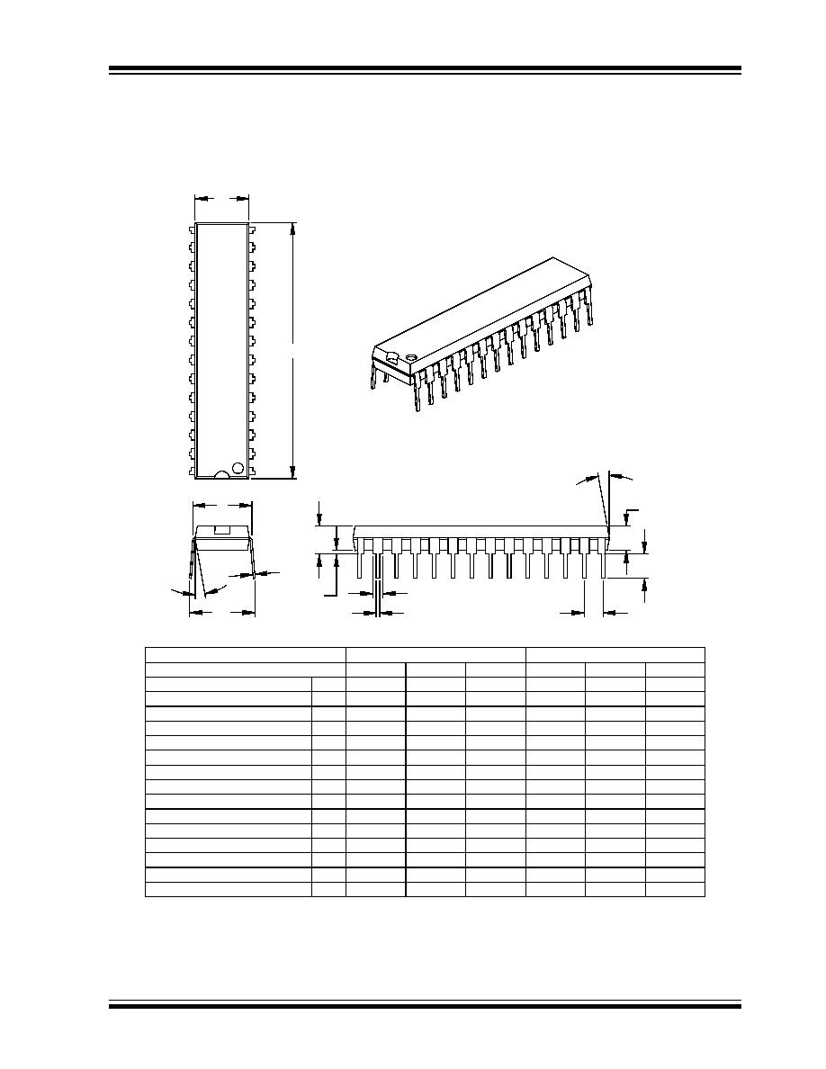
2002 Microchip Technology Inc.
Preliminary
DS41159B-page 359
PIC18FXX8
29.2
Package Details
The following sections give the technical details of the
packages.
28-Lead Skinny Plastic Dual In-line (SP) � 300 mil (PDIP)
15
10
5
15
10
5
Mold Draft Angle Bottom
15
10
5
15
10
5
Mold Draft Angle Top
10.92
8.89
8.13
.430
.350
.320
eB
Overall Row Spacing
�
0.56
0.48
0.41
.022
.019
.016
B
Lower Lead Width
1.65
1.33
1.02
.065
.053
.040
B1
Upper Lead Width
0.38
0.29
0.20
.015
.012
.008
c
Lead Thickness
3.43
3.30
3.18
.135
.130
.125
L
Tip to Seating Plane
35.18
34.67
34.16
1.385
1.365
1.345
D
Overall Length
7.49
7.24
6.99
.295
.285
.275
E1
Molded Package Width
8.26
7.87
7.62
.325
.310
.300
E
Shoulder to Shoulder Width
0.38
.015
A1
Base to Seating Plane
3.43
3.30
3.18
.135
.130
.125
A2
Molded Package Thickness
4.06
3.81
3.56
.160
.150
.140
A
Top to Seating Plane
2.54
.100
p
Pitch
28
28
n
Number of Pins
MAX
NOM
MIN
MAX
NOM
MIN
Dimension Limits
MILLIMETERS
INCHES*
Units
2
1
D
n
E1
c
eB
E
p
L
A2
B
B1
A
A1
Notes:
JEDEC Equivalent: MO-095
Drawing No. C04-070
* Controlling Parameter
Dimension D and E1 do not include mold flash or protrusions. Mold flash or protrusions shall not exceed
.010" (0.254mm) per side.
� Significant Characteristic
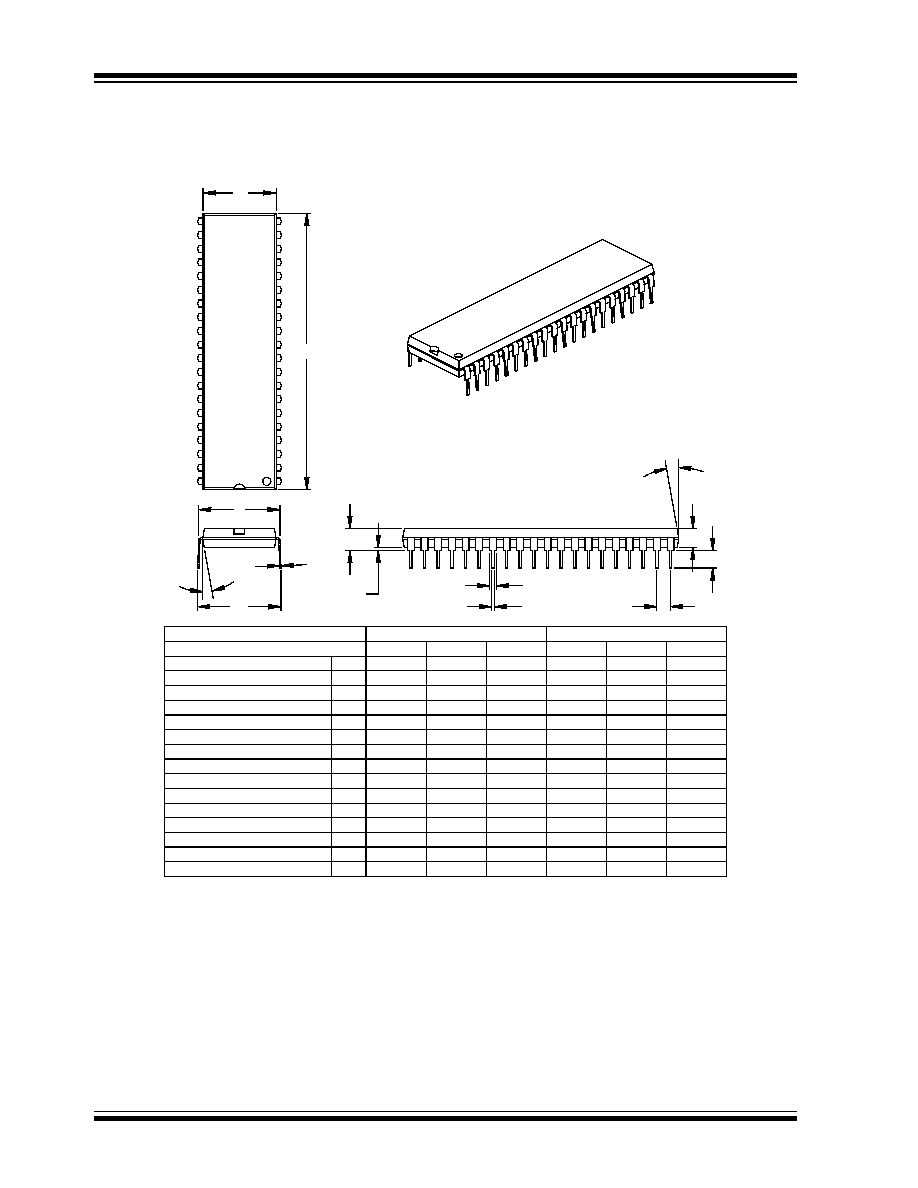
PIC18FXX8
DS41159B-page 360
Preliminary
2002 Microchip Technology Inc.
40-Lead Plastic Dual In-line (P) � 600 mil (PDIP)
15
10
5
15
10
5
Mold Draft Angle Bottom
15
10
5
15
10
5
Mold Draft Angle Top
17.27
16.51
15.75
.680
.650
.620
eB
Overall Row Spacing
�
0.56
0.46
0.36
.022
.018
.014
B
Lower Lead Width
1.78
1.27
0.76
.070
.050
.030
B1
Upper Lead Width
0.38
0.29
0.20
.015
.012
.008
c
Lead Thickness
3.43
3.30
3.05
.135
.130
.120
L
Tip to Seating Plane
52.45
52.26
51.94
2.065
2.058
2.045
D
Overall Length
14.22
13.84
13.46
.560
.545
.530
E1
Molded Package Width
15.88
15.24
15.11
.625
.600
.595
E
Shoulder to Shoulder Width
0.38
.015
A1
Base to Seating Plane
4.06
3.81
3.56
.160
.150
.140
A2
Molded Package Thickness
4.83
4.45
4.06
.190
.175
.160
A
Top to Seating Plane
2.54
.100
p
Pitch
40
40
n
Number of Pins
MAX
NOM
MIN
MAX
NOM
MIN
Dimension Limits
MILLIMETERS
INCHES*
Units
A2
1
2
D
n
E1
c
eB
E
p
L
B
B1
A
A1
* Controlling Parameter
Notes:
Dimensions D and E1 do not include mold flash or protrusions. Mold flash or protrusions shall not exceed
.010" (0.254mm) per side.
JEDEC Equivalent: MO-011
Drawing No. C04-016
� Significant Characteristic
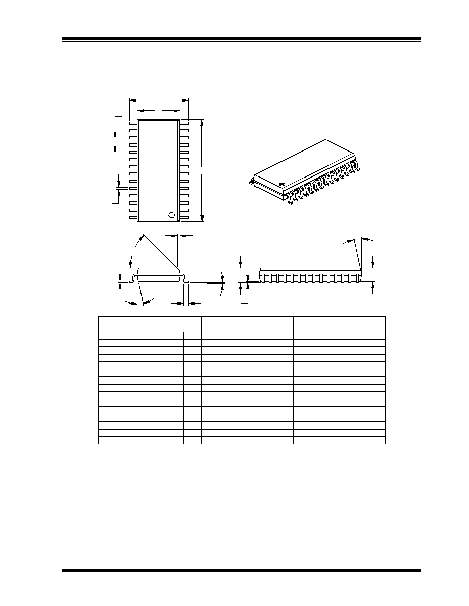
2002 Microchip Technology Inc.
Preliminary
DS41159B-page 361
PIC18FXX8
28-Lead Plastic Small Outline (SO) � Wide, 300 mil (SOIC)
Foot Angle Top
0
4
8
0
4
8
15
12
0
15
12
0
Mold Draft Angle Bottom
15
12
0
15
12
0
Mold Draft Angle Top
0.51
0.42
0.36
.020
.017
.014
B
Lead Width
0.33
0.28
0.23
.013
.011
.009
c
Lead Thickness
1.27
0.84
0.41
.050
.033
.016
L
Foot Length
0.74
0.50
0.25
.029
.020
.010
h
Chamfer Distance
18.08
17.87
17.65
.712
.704
.695
D
Overall Length
7.59
7.49
7.32
.299
.295
.288
E1
Molded Package Width
10.67
10.34
10.01
.420
.407
.394
E
Overall Width
0.30
0.20
0.10
.012
.008
.004
A1
Standoff
�
2.39
2.31
2.24
.094
.091
.088
A2
Molded Package Thickness
2.64
2.50
2.36
.104
.099
.093
A
Overall Height
1.27
.050
p
Pitch
28
28
n
Number of Pins
MAX
NOM
MIN
MAX
NOM
MIN
Dimension Limits
MILLIMETERS
INCHES*
Units
2
1
D
p
n
B
E
E1
L
c
45
�
h
A2
A
A1
* Controlling Parameter
Notes:
Dimensions D and E1 do not include mold flash or protrusions. Mold flash or protrusions shall not exceed
.010" (0.254mm) per side.
JEDEC Equivalent: MS-013
Drawing No. C04-052
� Significant Characteristic
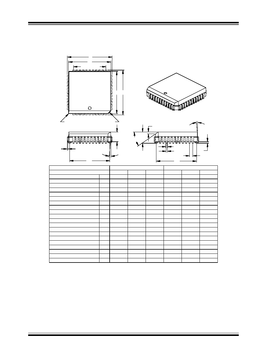
PIC18FXX8
DS41159B-page 362
Preliminary
2002 Microchip Technology Inc.
44-Lead Plastic Leaded Chip Carrier (L) � Square (PLCC)
CH2 x 45
�
CH1 x 45
�
10
5
0
10
5
0
Mold Draft Angle Bottom
10
5
0
10
5
0
Mold Draft Angle Top
0.53
0.51
0.33
.021
.020
.013
B
0.81
0.74
0.66
.032
.029
.026
B1
Upper Lead Width
0.33
0.27
0.20
.013
.011
.008
c
Lead Thickness
11
11
n1
Pins per Side
16.00
15.75
14.99
.630
.620
.590
D2
Footprint Length
16.00
15.75
14.99
.630
.620
.590
E2
Footprint Width
16.66
16.59
16.51
.656
.653
.650
D1
Molded Package Length
16.66
16.59
16.51
.656
.653
.650
E1
Molded Package Width
17.65
17.53
17.40
.695
.690
.685
D
Overall Length
17.65
17.53
17.40
.695
.690
.685
E
Overall Width
0.25
0.13
0.00
.010
.005
.000
CH2
Corner Chamfer (others)
1.27
1.14
1.02
.050
.045
.040
CH1
Corner Chamfer 1
0.86
0.74
0.61
.034
.029
.024
A3
Side 1 Chamfer Height
0.51
.020
A1
Standoff
�
A2
Molded Package Thickness
4.57
4.39
4.19
.180
.173
.165
A
Overall Height
1.27
.050
p
Pitch
44
44
n
Number of Pins
MAX
NOM
MIN
MAX
NOM
MIN
Dimension Limits
MILLIMETERS
INCHES*
Units
A2
c
E2
2
D
D1
n
#leads=n1
E
E1
1
p
A3
A
35
�
B1
B
D2
A1
.145
.153
.160
3.68
3.87
4.06
.028
.035
0.71
0.89
Lower Lead Width
* Controlling Parameter
Notes:
Dimensions D and E1 do not include mold flash or protrusions. Mold flash or protrusions shall not exceed
.010" (0.254mm) per side.
JEDEC Equivalent: MO-047
Drawing No. C04-048
� Significant Characteristic
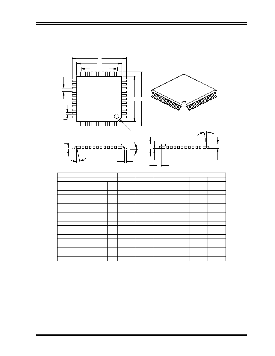
2002 Microchip Technology Inc.
Preliminary
DS41159B-page 363
PIC18FXX8
44-Lead Plastic Thin Quad Flatpack (PT) 10x10x1 mm Body, 1.0/0.10 mm Lead Form (TQFP)
* Controlling Parameter
Notes:
Dimensions D1 and E1 do not include mold flash or protrusions. Mold flash or protrusions shall not exceed
.010" (0.254mm) per side.
JEDEC Equivalent: MS-026
Drawing No. C04-076
1.14
0.89
0.64
.045
.035
.025
CH
Pin 1 Corner Chamfer
1.00
.039
(F)
Footprint (Reference)
(F)
A
A1
A2
E
E1
#leads=n1
p
B
D1
D
n
1
2
c
L
Units
INCHES
MILLIMETERS*
Dimension Limits
MIN
NOM
MAX
MIN
NOM
MAX
Number of Pins
n
44
44
Pitch
p
.031
0.80
Overall Height
A
.039
.043
.047
1.00
1.10
1.20
Molded Package Thickness
A2
.037
.039
.041
0.95
1.00
1.05
Standoff
�
A1
.002
.004
.006
0.05
0.10
0.15
Foot Length
L
.018
.024
.030
0.45
0.60
0.75
Foot Angle
0
3.5
7
0
3.5
7
Overall Width
E
.463
.472
.482
11.75
12.00
12.25
Overall Length
D
.463
.472
.482
11.75
12.00
12.25
Molded Package Width
E1
.390
.394
.398
9.90
10.00
10.10
Molded Package Length
D1
.390
.394
.398
9.90
10.00
10.10
Pins per Side
n1
11
11
Lead Thickness
c
.004
.006
.008
0.09
0.15
0.20
Lead Width
B
.012
.015
.017
0.30
0.38
0.44
Mold Draft Angle Top
5
10
15
5
10
15
Mold Draft Angle Bottom
5
10
15
5
10
15
CH x 45
�
� Significant Characteristic

PIC18FXX8
DS41159B-page 364
Preliminary
2002 Microchip Technology Inc.
NOTES:

2002 Microchip Technology Inc.
Preliminary
DS41159B-page 365
PIC18FXX8
APPENDIX A:
DATA SHEET
REVISION HISTORY
Revision A (June 2001)
Original data sheet for the PIC18FXX8 family.
Revision B (May 2002)
Updated information on CAN module, device memory
and register maps, I/O ports and Enhanced CCP.
APPENDIX B:
DEVICE
DIFFERENCES
The differences between the devices listed in this data
sheet are shown in Table B-1.
TABLE B-1:
DEVICE DIFFERENCES
Features
PIC18F248
PIC18F258
PIC18F448
PIC18F458
Internal
Program
Memory
Bytes
16K
32K
16K
32K
# of Single word
Instructions
8192
16384
8192
16384
Data Memory (Bytes)
768
1536
768
1536
I/O Ports
Ports A, B, C
Ports A, B, C
Ports A, B, C, D, E Ports A, B, C, D, E
Enhanced Capture/Compare/PWM
Modules
--
--
1
1
Parallel Slave Port
No
No
Yes
Yes
10-bit Analog-to-Digital Converter
5 input channels
5 input channels
8 input channels
8 input channels
Analog Comparators
No
No
2
2
Analog Comparators V
REF
Output
N/A
N/A
Yes
Yes
Packages
28-pin SPDIP
28-pin SOIC
28-pin SPDIP
28-pin SOIC
40-pin PDIP
44-pin PLCC
44-pin TQFP
40-pin PDIP
44-pin PLCC
44-pin TQFP

PIC18FXX8
DS41159B-page 366
Preliminary
2002 Microchip Technology Inc.
APPENDIX C:
DEVICE MIGRATIONS
This section is intended to describe the functional and
electrical specification differences when migrating
between functionally similar devices (such as from a
PIC16C74A to a PIC16C74B).
Not Applicable
APPENDIX D:
MIGRATING FROM
OTHER PICmicro
DEVICES
This discusses some of the issues in migrating from
other PICmicro devices to the PIC18FXX8 family of
devices.
D.1
PIC16CXXX to PIC18FXX8
See Application Note AN716.
D.2
PIC17CXXX to PIC18FXX8
See Application Note AN726.

2002 Microchip Technology Inc.
Preliminary
DS41159B-page 367
PIC18FXX8
APPENDIX E:
DEVELOPMENT
TOOL VERSION
REQUIREMENTS
This lists the minimum requirements (software/
firmware) of the specified development tool to support
the devices listed in this data sheet.
MPLAB
�
SIMULATOR:
V7.40 (MPLAB IDE V5.40)
MPLAB
�
ICE 2000:
MPLAB IDE
TBD
PIC18FXX8 Processor Module:
Part Number
PCM 18XD0
PIC18FXX8 Device Adapter:
Socket
Part Number
28-pin PDIP
DVA16XP282
28-pin SOIC
DVA16XP282 with
XLT 28SO Transition
Socket
40-pin PDIP
DVA16XP401
44-pin TQFP
DVA16PQ441 with
XLT 44PT Transition
Socket
44-pin PLCC
DVA16XL441
MPLAB
�
ICD 2:
TBD
PRO MATE
�
II:
TBD
Device Programmer
PICSTART
�
Plus:
version TBD
Development Programmer
MPASM
TM
Assembler:
V2.80
(MPLAB IDE V5.40)
MPLAB
�
C18 C Compiler:
version TBD
CAN-TOOL:
Not available at time of
printing.
Third Party Tools:
OSEK/VDX operating
system available from
Vector Infromatik GmbH,
Germany and Realogy
Ltd, UK.
Note:
Please read all associated
README.TXT
files that are supplied with the develop-
ment tools. These "read me" files will dis-
cuss product support and any known
limitations.

PIC18FXX8
DS41159B-page 368
Preliminary
2002 Microchip Technology Inc.
NOTES:

2002 Microchip Technology Inc.
Preliminary
DS41159B-page 369
PIC18FXX8
INDEX
A
A/D
................................................................................... 237
A/D Converter Flag (ADIF bit)
.................................. 239
A/D Converter Interrupt, Configuring
....................... 240
Acquisition Requirements
........................................ 240
Acquisition Time
....................................................... 241
ADCON0 Register
.................................................... 237
ADCON1 Register
.................................................... 237
ADRESH Register
.................................................... 237
ADRESH/ADRESL Registers
.................................. 239
ADRESL Register
.................................................... 237
Analog Port Pins, Configuring
.................................. 242
Associated Registers Summary
............................... 243
Calculating the Minimum Required
Acquisition Time
............................................... 241
Configuring the Module
............................................ 240
Conversion Clock (T
AD
)
........................................... 242
Conversion Status (GO/DONE bit)
.......................... 239
Conversion T
AD
Cycles
............................................ 243
Conversions
............................................................. 243
Converter Characteristics
........................................ 352
Minimum Charging Time
.......................................... 241
Selecting the Conversion Clock
............................... 242
Special Event Trigger (CCP)
.................................... 124
Special Event Trigger (ECCP)
......................... 131
,
243
T
AD
vs. Device Operating Frequencies
(For Extended, LC Devices) (table)
................. 242
T
AD
vs. Device Operating Frequencies (table)
........ 242
Use of the ECCP Trigger
......................................... 243
Absolute Maximum Ratings
............................................. 325
AC (Timing) Characteristics
............................................. 335
Parameter Symbology
............................................. 335
Access Bank
...................................................................... 54
ACKSTAT
......................................................................... 171
ADCON0 Register
............................................................ 237
GO/DONE bit
........................................................... 239
ADCON1 Register
............................................................ 237
ADDLW
............................................................................ 283
Addressable Universal Synchronous Asynchronous
Receiver Transmitter. See USART
ADDWF
............................................................................ 283
ADDWFC
......................................................................... 284
ADRESH Register
............................................................ 237
ADRESH/ADRESL Registers
........................................... 239
ADRESL Register
............................................................ 237
Analog-to-Digital Converter. See A/D
ANDLW
............................................................................ 284
ANDWF
............................................................................ 285
Assembler
MPASM Assembler
.................................................. 319
Associated Registers
............................................... 190
,
195
B
Bank Select Register (BSR)
............................................... 54
Baud Rate Generator
....................................................... 167
BC
.................................................................................... 285
BCF
.................................................................................. 286
BF
..................................................................................... 171
Bit Timing Configuration Registers
BRGCON1
............................................................... 232
BRGCON2
............................................................... 232
BRGCON3
............................................................... 232
Block Diagrams
A/D
........................................................................... 239
Analog Input Model
...........................................240
,
249
Baud Rate Generator
.............................................. 167
CAN Buffers and Protocol Engine
........................... 198
Capture Mode (CCP Module)
.................................. 123
Comparator I/O Operating Modes
........................... 246
Comparator Output
.................................................. 248
Compare (CCP Module) Mode Operation
............... 124
Enhanced PWM
....................................................... 132
Interrupt Logic
............................................................ 78
Low Voltage Detect
................................................. 256
Low Voltage Detect with External Input
................... 256
MSSP (I
2
C Master Mode)
........................................ 165
MSSP (I
2
C Mode)
.................................................... 150
MSSP (SPI Mode)
................................................... 141
On-Chip Reset Circuit
................................................ 25
PIC18F248/258 Architecture
....................................... 8
PIC18F448/458 Architecture
....................................... 9
PLL
............................................................................ 19
PORTC (Peripheral Output Override)
........................ 98
PORTD and PORTE (Parallel Slave Port)
............... 105
PORTD in I/O Port Mode
......................................... 100
PORTE
.................................................................... 102
PWM (CCP Module)
................................................ 126
RA3:RA0 and RA5 Port Pins
..................................... 93
RA4/T0CKI Pin
.......................................................... 93
RA6/OSC2/CLKO Pin
................................................ 94
RB1:RB0 Port Pins
.................................................... 95
RB2:CANTX Port Pins
............................................... 96
RB3:CANRX Port Pins
............................................... 96
RB7:RB4 Port Pins
.................................................... 95
Reads from FLASH Program Memory
....................... 69
Receive Buffer
......................................................... 226
Table Read Operation
............................................... 65
Table Write Operation
................................................ 66
Table Writes to FLASH Program Memory
................. 71
Timer0 Module
16-bit Mode
...................................................... 108
8-bit Mode
........................................................ 108
Timer1 Module
......................................................... 112
Timer1 Module (16-bit Read/Write Mode)
............... 112
Timer2
..................................................................... 116
Timer3
..................................................................... 118
Timer3 (16-bit Read/Write Mode)
............................ 118
Transmit Buffer
........................................................ 223
USART Receive
....................................................... 189
USART Transmit
...................................................... 187
Voltage Reference
................................................... 252
Watchdog Timer
...................................................... 269
BN
.................................................................................... 286
BNC
................................................................................. 287
BNN
................................................................................. 287
BNOV
............................................................................... 288
BNZ
.................................................................................. 288
BOR. See Brown-out Reset
BOV
................................................................................. 291
BRA
................................................................................. 289

PIC18FXX8
DS41159B-page 370
Preliminary
2002 Microchip Technology Inc.
BRG. See Baud Rate Generator
Brown-out Reset (BOR)
............................................. 26
,
261
BSF
.................................................................................. 289
BTFSC
............................................................................. 290
BTFSS
.............................................................................. 290
BTG
.................................................................................. 291
BZ
..................................................................................... 292
C
CALL
................................................................................ 292
CAN Module
..................................................................... 197
Aborting Transmission
............................................. 224
Acknowledge Error
................................................... 233
Baud Rate Registers
................................................ 215
Baud Rate Setting
.................................................... 229
Bit Error
.................................................................... 233
Bit Time Partitioning
................................................. 229
Bit Timing Configuration Registers
........................... 232
Calculating T
Q
, Nominal bit Rate and
Nominal bit Time
.............................................. 230
Configuration Mode
.................................................. 222
Control and Status Registers
................................... 199
Controller Register Map
........................................... 221
CRC Error
................................................................ 233
Disable Mode
........................................................... 222
Error Detection
......................................................... 233
Error Modes and Error Counters
.............................. 233
Error Modes State Diagram
..................................... 234
Error States
.............................................................. 233
Filter Mask Truth (table)
........................................... 228
Form Error
................................................................ 233
Hard Synchronization
............................................... 231
I/O Control Register
................................................. 217
Information Processing Time
................................... 230
Initiating Transmission
............................................. 224
Interrupt Acknowledge
............................................. 235
Interrupt Registers
.................................................... 218
Interrupts
.................................................................. 234
Bus Activity Wake-up
....................................... 235
Bus-Off
............................................................. 235
Code bits
.......................................................... 234
Error
................................................................. 235
Message Error
................................................. 235
Receive
............................................................ 234
Receiver Bus Passive
...................................... 235
Receiver Overflow
............................................ 235
Receiver Warning
............................................ 235
Transmit
........................................................... 234
Transmitter Bus Passive
.................................. 235
Transmitter Warning
........................................ 235
Lengthening a bit Period
.......................................... 231
Listen Only Mode
..................................................... 222
Loopback Mode
........................................................ 223
Message Acceptance Filters and
Masks
....................................................... 212
,
228
Message Acceptance Mask and
Filter Operation
................................................ 228
Message Reception
................................................. 226
Message Reception Flow Chart
............................... 227
Message Time-Stamping
......................................... 226
Message Transmission
............................................ 223
Modes of Operation
.................................................. 222
Normal Mode
............................................................ 222
Oscillator Tolerance
................................................. 232
Overview
.................................................................. 197
Phase Buffer Segments
........................................... 230
Programming Time Segments
................................. 232
Propagation Segment
.............................................. 230
Receive Buffer Registers
......................................... 208
Receive Buffers
....................................................... 226
Receive Message Buffering
..................................... 226
Receive Priority
........................................................ 226
Registers
.................................................................. 199
Resynchronization
................................................... 231
Sample Point
........................................................... 230
Shortening a bit Period
............................................ 232
Stuff Bit Error
........................................................... 233
Synchronization
....................................................... 231
Synchronization Rules
............................................. 231
Synchronization Segment
........................................ 230
Time Quanta
............................................................ 230
Transmit Buffer Registers
........................................ 204
Transmit Buffers
...................................................... 223
Transmit Message Flow Chart
................................. 225
Transmit Priority
....................................................... 223
Transmit/Receive Buffers
........................................ 197
Values for ICODE (table)
......................................... 235
Capture (CCP Module)
.................................................... 122
CAN Message Time-Stamp
..................................... 123
CCP Pin Configuration
............................................. 122
CCPR1H:CCPR1L Registers
................................... 122
Software Interrupt
.................................................... 123
Timer1/Timer3 Mode Selection
................................ 122
Capture (ECCP Module)
.................................................. 131
CAN Message Time-Stamp
..................................... 131
Capture/Compare/PWM (CCP)
........................................ 121
Capture Mode. See Capture (CCP Module)
CCP1 Module
.......................................................... 122
CCPR1H Register
.................................................... 122
CCPR1L Register
.................................................... 122
Compare Mode. See Compare (CCP Module)
Interaction of CCP1 and ECCP1 Modules
............... 122
PWM Mode. See PWM (CCP Module)
Timer Resources
..................................................... 122
Ceramic Resonators
Ranges Tested
.......................................................... 17
Clocking Scheme
............................................................... 41
CLRF
............................................................................... 293
CLRWDT
.......................................................................... 293
Code Examples
16 x 16 Signed Multiply Routine
................................ 76
16 x 16 Unsigned Multiply Routine
............................ 76
8 x 8 Signed Multiply Routine
.................................... 75
8 x 8 Unsigned Multiply Routine
................................ 75
Changing Between Capture Prescalers
................... 123
Data EEPROM Read
................................................. 61
Data EEPROM Refresh Routine
................................ 62
Data EEPROM Write
................................................. 61
Erasing a FLASH Program Memory Row
.................. 70
Fast Register Stack
................................................... 40
How to Clear RAM (Bank 1) Using
Indirect Addressing
............................................ 55
Initializing PORTA
...................................................... 93
Initializing PORTB
...................................................... 95
Initializing PORTC
..................................................... 98
Initializing PORTD
................................................... 100
Initializing PORTE
.................................................... 102
Loading the SSPBUF Register
................................ 144
Reading a FLASH Program Memory Word
............... 69
Saving STATUS, WREG and
BSR Registers in RAM
...................................... 92

2002 Microchip Technology Inc.
Preliminary
DS41159B-page 371
PIC18FXX8
WIN and ICODE bits Usage in Interrupt
Service Routine to Access TX/RX Buffers
....... 201
Writing to FLASH Program Memory
.................... 72
�
73
Code Protection
............................................................... 261
COMF
............................................................................... 294
Comparator Module
......................................................... 245
Analog Input Connection Considerations
................. 249
Associated Registers
............................................... 250
Configuration
............................................................ 246
Effects of a RESET
.................................................. 249
External Reference Signal
....................................... 247
Internal Reference Signal
........................................ 247
Interrupts
.................................................................. 248
Operation
................................................................. 247
Operation During SLEEP
......................................... 249
Outputs
.................................................................... 247
Reference
................................................................ 247
Response Time
........................................................ 247
Comparator Specifications
............................................... 334
Comparator Voltage Reference Module
........................... 251
Accuracy/Error
......................................................... 252
Associated Registers
............................................... 253
Configuring
............................................................... 251
Connection Considerations
...................................... 252
Effects of a RESET
.................................................. 252
Operation During SLEEP
......................................... 252
Output Buffer Example
............................................. 253
Compare (CCP Module)
................................................... 124
Associated Registers
............................................... 125
CCP1 Pin Configuration
........................................... 124
CCPR1H:CCPR1L Registers
................................... 124
Software Interrupt
.................................................... 124
Special Event Trigger
........................113
,
119
,
124
,
243
Timer1/Timer3 Mode Selection
................................ 124
Compare (ECCP Module)
................................................ 131
Associated Registers
............................................... 131
Special Event Trigger
............................................... 131
Compatible 10-bit Analog-to-Digital Converter
(A/D) Module. See A/D.
Configuration Mode (CAN Module)
.................................. 222
CPFSEQ
.......................................................................... 294
CPFSGT
........................................................................... 295
CPFSLT
........................................................................... 295
Crystal Oscillator
Capacitor Selection
.................................................... 18
D
Data EEPROM Memory
..................................................... 59
Associated Registers
................................................. 63
EEADR Register
........................................................ 59
EECON1 Register
...................................................... 59
EECON2 Register
...................................................... 59
Operation During Code Protect
.................................. 62
Protection Against Spurious Writes
........................... 62
Reading
...................................................................... 61
Usage
......................................................................... 62
Write Verify
................................................................ 62
Writing to
.................................................................... 61
Data Memory
...................................................................... 44
General Purpose Registers
........................................ 44
Special Function Registers
........................................ 44
Data Memory Map
PIC18F248/448
.......................................................... 45
PIC18F258/458
.......................................................... 46
DAW
................................................................................. 296
DC and AC Characteristics Graphs and Tables
............... 355
DC Characteristics
............................ 327
,
328
,
329
,
330
,
331
EEPROM and Enhanced FLASH
............................ 333
DCFSNZ
.......................................................................... 297
DECF
............................................................................... 296
DECFSZ
.......................................................................... 297
Development Support
...................................................... 319
Development Tool Version Requirements
....................... 367
Device Differences
........................................................... 365
Device Migrations
............................................................ 366
Device Overview
.................................................................. 7
Features
...................................................................... 7
Direct Addressing
.............................................................. 56
Disable Mode (CAN Module)
........................................... 222
E
Electrical Characteristics
................................................. 325
Enhanced Capture/Compare/PWM (ECCP)
.................... 129
Auto-Shutdown
........................................................ 140
Capture Mode. See Capture (ECCP Module)
Compare Mode. See Compare (ECCP Module)
ECCPR1H Register
................................................. 130
ECCPR1L Register
.................................................. 130
Interaction of CCP1 and ECCP1 Modules
............... 130
Pin Assignments for Various Modes
........................ 130
PWM Mode. See PWM (ECCP Module)
Timer Resources
..................................................... 130
Enhanced CCP Auto-Shutdown
...................................... 140
Enhanced PWM Mode. See PWM
(ECCP Module)
........................................................ 132
Errata
................................................................................... 5
Error Recognition Mode (CAN Module)
........................... 222
External Clock Input
........................................................... 19
F
Firmware Instructions
...................................................... 277
FLASH Program Memory
.................................................. 65
Associated Registers
................................................. 74
Control Registers
....................................................... 66
Erase Sequence
........................................................ 70
Erasing
...................................................................... 70
Operation During Code Protect
................................. 73
Reading
..................................................................... 69
TABLAT (Table Latch) Register
................................. 68
Table Pointer
Boundaries Based on Operation
....................... 68
Table Pointer Boundaries
.......................................... 68
Table Reads and Table Writes
.................................. 65
TBLPTR (Table Pointer) Register
.............................. 68
Write Sequence
......................................................... 71
Writing to
................................................................... 71
Protection Against Spurious Writes
................... 73
Unexpected Termination
................................... 73
Write Verify
........................................................ 73
G
GOTO
.............................................................................. 298
H
Hardware Multiplier
............................................................ 75
Operation
................................................................... 75
Performance Comparison (table)
............................... 75
HS4 (PLL)
.......................................................................... 19

PIC18FXX8
DS41159B-page 372
Preliminary
2002 Microchip Technology Inc.
I
I/O Ports
............................................................................. 93
I
2
C Mode
.......................................................................... 150
ACK Pulse
........................................................ 154
,
155
Acknowledge Sequence Timing
............................... 174
Baud Rate Generator
............................................... 167
Bus Collision and Arbitration
.................................... 175
Bus Collision During a Repeated
START Condition
............................................. 179
Bus Collision During a START Condition
................. 177
Bus Collision During a STOP Condition
................... 180
Clock Arbitration
....................................................... 168
Clock Stretching
....................................................... 160
Effect of a RESET
.................................................... 175
General Call Address Support
................................. 164
Master Mode
............................................................ 165
Operation
......................................................... 166
Reception
......................................................... 171
Repeated START Condition Timing
................. 170
Master Mode START Condition Timing
................... 169
Master Mode Transmission
...................................... 171
Multi-Master Mode
................................................... 175
Read/Write bit Information (R/W bit)
................ 154
,
155
Registers
.................................................................. 150
Serial Clock (RC3/SCK/SCL)
................................... 155
Slave Mode
.............................................................. 154
Addressing
....................................................... 154
Reception
......................................................... 155
Transmission
.................................................... 155
SLEEP Operation
..................................................... 175
STOP Condition Timing
........................................... 174
ICEPIC In-Circuit Emulator
.............................................. 320
ID Locations
............................................................. 261
,
275
INCF
................................................................................. 298
INCFSZ
............................................................................ 299
In-Circuit Debugger
.......................................................... 275
In-Circuit Serial Programming (ICSP)
...................... 261
,
275
Indirect Addressing
............................................................ 56
FSR Register
.............................................................. 55
INDF Register
............................................................ 55
Operation
................................................................... 55
INFSNZ
............................................................................ 299
Initialization Conditions for All Registers
............................ 30
Instruction Cycle
................................................................. 41
Instruction Flow/Pipelining
................................................. 41
Instruction Format
............................................................ 279
Instruction Set
.................................................................. 277
ADDLW
.................................................................... 283
ADDWF
.................................................................... 283
ADDWFC
................................................................. 284
ANDLW
.................................................................... 284
ANDWF
.................................................................... 285
BC
............................................................................ 285
BCF
.......................................................................... 286
BN
............................................................................ 286
BNC
.......................................................................... 287
BNN
.......................................................................... 287
BNOV
....................................................................... 288
BNZ
.......................................................................... 288
BOV
.......................................................................... 291
BRA
.......................................................................... 289
BSF
.......................................................................... 289
BTFSC
..................................................................... 290
BTFSS
...................................................................... 290
BTG
.......................................................................... 291
BZ
............................................................................ 292
CALL
........................................................................ 292
CLRF
....................................................................... 293
CLRWDT
................................................................. 293
COMF
...................................................................... 294
CPFSEQ
.................................................................. 294
CPFSGT
.................................................................. 295
CPFSLT
................................................................... 295
DAW
........................................................................ 296
DCFSNZ
.................................................................. 297
DECF
....................................................................... 296
DECFSZ
.................................................................. 297
GOTO
...................................................................... 298
INCF
........................................................................ 298
INCFSZ
.................................................................... 299
INFSNZ
.................................................................... 299
IORLW
..................................................................... 300
IORWF
..................................................................... 300
LFSR
........................................................................ 301
MOVF
...................................................................... 301
MOVFF
.................................................................... 302
MOVLB
.................................................................... 302
MOVLW
................................................................... 303
MOVWF
................................................................... 303
MULLW
.................................................................... 304
MULWF
.................................................................... 304
NEGF
....................................................................... 305
NOP
......................................................................... 305
POP
......................................................................... 306
PUSH
....................................................................... 306
RCALL
..................................................................... 307
RESET
..................................................................... 307
RETFIE
.................................................................... 308
RETLW
.................................................................... 308
RETURN
.................................................................. 309
RLCF
....................................................................... 309
RLNCF
..................................................................... 310
RRCF
....................................................................... 310
RRNCF
.................................................................... 311
SETF
........................................................................ 311
SLEEP
..................................................................... 312
SUBFWB
................................................................. 312
SUBLW
.................................................................... 313
SUBWF
.................................................................... 313
SUBWFB
................................................................. 314
SWAPF
.................................................................... 314
TBLRD
..................................................................... 315
TBLWT
..................................................................... 316
TSTFSZ
................................................................... 317
XORLW
.................................................................... 317
XORWF
................................................................... 318
Summary Table
....................................................... 280
INTCON Register
RBIF bit
...................................................................... 95
Inter-Integrated Circuit. See I
2
C
Interrupt Sources
A/D Conversion Complete
....................................... 240
CAN Module
............................................................ 234
Capture Complete (CCP)
......................................... 123
Compare Complete (CCP)
....................................... 124
Interrupt-on-Change (RB7:RB4)
................................ 95
TMR0 Overflow
........................................................ 109
TMR1 Overflow
.................................................111
,
113
TMR2 to PR2 Match
................................................ 116
TMR2 to PR2 Match (PWM)
.............................115
,
126
TMR3 Overflow
.................................................117
,
119

2002 Microchip Technology Inc.
Preliminary
DS41159B-page 373
PIC18FXX8
Interrupt-on-Change (RB7:RB4) Flag
(RBIF bit)
.................................................................... 95
Interrupts
............................................................................ 77
Context Saving During
............................................... 92
Enable Registers
........................................................ 85
Flag Registers
............................................................ 82
INT
............................................................................. 92
PORTB Interrupt-on-Change
..................................... 92
Priority Registers
........................................................ 88
TMR0
......................................................................... 92
Interrupts, Flag bits
CCP1 Flag (CCP1IF bit)
...........................122
,
123
,
124
Interrupts, Flag bits
A/D Converter Flag (ADIF bit)
.................................. 239
IORLW
............................................................................. 300
IORWF
............................................................................. 300
K
K
EE
L
OQ
Evaluation and Programming Tools
................... 322
L
LFSR
................................................................................ 301
Listen Only Mode (CAN Module)
..................................... 222
Lookup Tables
.................................................................... 43
Computed GOTO
....................................................... 43
Table Reads/Table Writes
......................................... 43
Loopback Mode (CAN Module)
........................................ 222
Low Voltage Detect
.......................................................... 255
Characteristics
......................................................... 332
Characteristics (diagram)
......................................... 332
Current Consumption
............................................... 259
Effects of a RESET
.................................................. 259
Operation
................................................................. 258
Operation During SLEEP
......................................... 259
Reference Voltage Set Point
.................................... 259
Typical Application
................................................... 255
Low Voltage ICSP Programming
..................................... 275
LVD. See Low Voltage Detect.
M
Master Synchronous Serial Port (MSSP). See MSSP.
Master Synchronous Serial Port. See MSSP.
Memory Organization
......................................................... 37
Data Memory
............................................................. 44
Internal Program Memory Operation
......................... 37
Program Memory
....................................................... 37
Migrating from other PICmicro Devices
........................... 366
MOVF
............................................................................... 301
MOVFF
............................................................................. 302
MOVLB
............................................................................. 302
MOVLW
............................................................................ 303
MOVWF
........................................................................... 303
MPLAB C17 and MPLAB C18 C Compilers
..................... 319
MPLAB ICD In-Circuit Debugger
...................................... 321
MPLAB ICE High Performance Universal
In-Circuit Emulator with MPLAB IDE
........................ 320
MPLAB Integrated Development
Environment Software
.............................................. 319
MPLINK Object Linker/MPLIB Object Librarian
............... 320
MSSP
............................................................................... 141
Control Registers
..................................................... 141
Enabling SPI I/O
...................................................... 145
I
2
C Mode Operation
................................................. 154
Operation
................................................................. 144
Overview
.................................................................. 141
SPI Master Mode
..................................................... 146
SPI Master/Slave Connection
.................................. 145
SPI Mode
................................................................. 141
SPI Slave Mode
....................................................... 147
TMR2 Output for Clock Shift
.............................115
,
116
Typical Connection
.................................................. 145
MSSP. See also I
2
C Mode, SPI Mode.
MULLW
............................................................................ 304
MULWF
............................................................................ 304
N
NEGF
............................................................................... 305
NOP
................................................................................. 305
Normal Operation Mode (CAN Module)
........................... 222
O
OPCODE Field Descriptions
............................................ 278
OPTION_REG Register
PSA bit
..................................................................... 109
T0CS bit
................................................................... 109
T0PS2:T0PS0 bits
................................................... 109
T0SE bit
................................................................... 109
Oscillator
Effects of SLEEP Mode
............................................. 23
Power-up Delays
....................................................... 23
Switching Feature
...................................................... 20
System Clock Switch bit
............................................ 20
Transitions
................................................................. 21
Oscillator Configurations
.................................................... 17
Crystal Oscillator, Ceramic Resonators
..................... 17
EC
.............................................................................. 17
ECIO
.......................................................................... 17
HS
.............................................................................. 17
HS4
............................................................................ 17
LP
.............................................................................. 17
RC
........................................................................17
,
18
RCIO
.......................................................................... 17
XT
.............................................................................. 17
Oscillator Selection
.......................................................... 261
Oscillator, Timer1
.............................................. 111
,
113
,
119
Oscillator, WDT
................................................................ 268
P
Packaging Information
..................................................... 357
Details
...................................................................... 359
Marking
.................................................................... 357
Parallel Slave Port (PSP)
..........................................100
,
105
Associated Registers
............................................... 106
PORTD
.................................................................... 105
PSP Mode Select (PSPMODE) bit
.......................... 100
RE2/CS
.................................................................... 105
PIC18FXX8 Voltage-Frequency Graph
(Industrial)
................................................................ 326
PIC18LFXX8 Voltage-Frequency Graph
(Industrial)
................................................................ 326
PICDEM 1 Low Cost PICmicro
Demonstration Board
............................................... 321
PICDEM 17 Demonstration Board
................................... 322
PICDEM 2 Low Cost PIC16CXX
Demonstration Board
............................................... 321
PICDEM 3 Low Cost PIC16CXXX
Demonstration Board
............................................... 322
PICSTART Plus Entry Level Development
Programmer
............................................................. 321

PIC18FXX8
DS41159B-page 374
Preliminary
2002 Microchip Technology Inc.
Pin Functions
MCLR/V
PP
.................................................................. 10
OSC1/CLKI
................................................................ 10
OSC2/CLKO/RA6
....................................................... 10
RA0/AN0/CV
REF
........................................................ 11
RA1/AN1
.................................................................... 11
RA2/AN2/V
REF
-
.......................................................... 11
RA3/AN3/V
REF
+
......................................................... 11
RA4/T0CKI
................................................................. 11
RA5/AN4/SS/LVDIN
................................................... 11
RA6
............................................................................ 11
RB0/INT0
................................................................... 12
RB1/INT1
................................................................... 12
RB2/CANTX
............................................................... 12
RB3/CANRX
............................................................... 12
RB4
............................................................................ 12
RB5/PGM
................................................................... 12
RB6/PGC
................................................................... 12
RB7/PGD
................................................................... 12
RC0/T1OSO/T1CKI
.................................................... 13
RC1/T1OSI
................................................................. 13
RC2/CCP1
................................................................. 13
RC3/SCK/SCL
............................................................ 13
RC4/SDI/SDA
............................................................. 13
RC5/SDO
................................................................... 13
RC6/TX/CK
................................................................ 13
RC7/RX/DT
................................................................ 13
RD0/PSP0/C1IN+
...................................................... 14
RD1/PSP1/C1IN-
....................................................... 14
RD2/PSP2/C2IN+
...................................................... 14
RD3/PSP3/C2IN-
....................................................... 14
RD4/PSP4/ECCP/PA
................................................. 14
RD5/PSP5/PB
............................................................ 14
RD6/PSP6/PC
............................................................ 14
RD7/PSP7/PD
............................................................ 14
RE0/AN5/RD
.............................................................. 15
RE1/AN6/WR/C1OUT
................................................ 15
RE2/AN7/CS/C2OUT
................................................. 15
Pinout I/O Descriptions
...................................................... 10
Pointer, FSRn
..................................................................... 55
POP
.................................................................................. 306
POR. See Power-on Reset.
PORTA
Associated Register Summary
................................... 94
Functions
.................................................................... 94
LATA Register
............................................................ 93
PORTA Register
........................................................ 93
TRISA Register
.......................................................... 93
PORTB
Associated Registers
................................................. 97
Functions
.................................................................... 97
LATB Register
............................................................ 95
PORTB Register
........................................................ 95
RB7:RB4 Interrupt-on-Change Flag
(RBIF bit)
............................................................ 95
TRISB Register
.......................................................... 95
PORTC
Associated Registers
................................................. 99
Functions
.................................................................... 99
LATC Register
............................................................ 98
PORTC Register
........................................................ 98
RC3/SCK/SCL Pin
................................................... 155
RC7/RX/DT Pin
........................................................ 183
TRISC Register
.................................................. 98
,
181
PORTD
Associated Register Summary
................................ 101
Functions
................................................................. 101
LATD Register
......................................................... 100
Parallel Slave Port (PSP) Function
.......................... 100
PORTD Register
...................................................... 100
TRISD Register
........................................................ 100
PORTE
Associated Register Summary
................................ 104
Functions
................................................................. 103
LATE Register
......................................................... 102
PORTE Register
...................................................... 102
PSP Mode Select (PSPMODE) bit
.......................... 100
RE2/CS
.................................................................... 105
TRISE Register
........................................................ 102
Postscaler, WDT
Assignment (PSA bit)
............................................... 109
Rate Select (T0PS2:T0PS0 bits)
............................. 109
Power-down Mode. See SLEEP
Power-on Reset (POR)
...............................................26
,
261
MCLR
......................................................................... 26
Oscillator Start-up Timer (OST)
..........................26
,
261
PLL Lock Time-out
..................................................... 26
Power-up Timer (PWRT)
....................................26
,
261
Time-out Sequence
................................................... 27
Power-up Delays
OSC1 and OSC2 Pin States in SLEEP Mode
........... 23
Prescaler, Capture
........................................................... 123
Prescaler, Timer0
............................................................. 109
Assignment (PSA bit)
............................................... 109
Rate Select (T0PS2:T0PS0 bits)
............................. 109
Prescaler, Timer2
............................................................. 126
PRO MATE II Universal Device Programmer
.................. 321
Product Identification System
.......................................... 381
Program Counter
PCL Register
............................................................. 40
PCLATH Register
...................................................... 40
PCLATU Register
...................................................... 40
Program Memory
............................................................... 37
Fast Register Stack
................................................... 40
Instructions
................................................................ 41
Two-Word
.......................................................... 43
Map and Stack for PIC18F248/448
........................... 37
Map and Stack for PIC18F258/458
........................... 37
PUSH and POP Instructions
...................................... 40
Return Address Stack
................................................ 38
Return Stack Pointer (STKPTR)
................................ 38
Stack Full/Underflow Resets
...................................... 40
Top-of-Stack Access
.................................................. 38
Program Verification and Code Protection
....................... 272
Associated Registers Summary
............................... 272
Configuration Register Protection
............................ 275
Data EEPROM Code Protection
.............................. 275
Program Memory Code Protection
.......................... 273
Programming, Device Instructions
................................... 277
PUSH
............................................................................... 306
PWM (CCP Module)
........................................................ 126
CCPR1H:CCPR1L Registers
................................... 126
Duty Cycle
............................................................... 126
Example Frequencies/Resolutions
.......................... 127
Output Diagram
....................................................... 126
Period
...................................................................... 126
Registers Associated with PWM and Timer2
........... 127
Setup for PWM Operation
........................................ 127
TMR2 to PR2 Match
.........................................115
,
126

2002 Microchip Technology Inc.
Preliminary
DS41159B-page 375
PIC18FXX8
PWM (ECCP Module)
...................................................... 132
Associated Registers
............................................... 139
Direction Change in Full-Bridge Output Mode
......... 136
Enhanced CCP Auto-Shutdown
............................... 140
Full-Bridge Application Example
.............................. 136
Full-Bridge Mode
...................................................... 135
Full-Bridge PWM Output Diagram
........................... 135
Half-Bridge Mode
..................................................... 134
Half-Bridge Output Diagram
..................................... 134
Half-Bridge Output Mode Applications Example
...... 134
Output Configurations
.............................................. 132
Output Polarity Configuration
................................... 138
Output Relationships Diagram
................................. 133
Programmable Deadband Delay
.............................. 138
PWM Direction Change at Near 100%
Duty Cycle Diagram
......................................... 137
PWM Direction Change Diagram
............................. 137
Setup for PWM Operation
........................................ 139
Standard Mode
........................................................ 132
Start-up Considerations
........................................... 138
System Implementation
........................................... 138
Q
Q Clock
............................................................................ 126
R
RAM. See Data Memory.
RCALL
.............................................................................. 307
RCON Register
Significance of Status bits vs.
Initialization Condition
........................................ 27
RCSTA Register
............................................................... 181
SPEN bit
.................................................................. 181
Receiver Warning
............................................................. 235
Register File
....................................................................... 44
Register File Summary
....................................................... 49
Registers
ADCON0 (A/D Control 0)
......................................... 237
ADCON1 (A/D Control 1)
......................................... 238
BRGCON1 (Baud Rate Control 1)
........................... 215
BRGCON2 (Baud Rate Control 2)
........................... 216
BRGCON3 (Baud Rate Control 3)
........................... 217
CANCON (CAN Control)
.......................................... 199
CANSTAT (CAN Status)
.......................................... 200
CCP1CON (CCP1 Control)
...................................... 121
CIOCON (CAN I/O Control)
..................................... 217
CMCON (Comparator Control)
................................ 245
COMSTAT (CAN Communication Status)
............... 203
CONFIG1H (Configuration 1 High)
.......................... 262
CONFIG2H (Configuration 2 High)
.......................... 263
CONFIG2L (Configuration 2 Low)
............................ 262
CONFIG4L (Configuration 4 Low)
............................ 263
CONFIG5H (Configuration 5 High)
.......................... 264
CONFIG5L (Configuration 5 Low)
............................ 264
CONFIG6H (Configuration 6 High)
.......................... 265
CONFIG6L (Configuration 6 Low)
............................ 265
CONFIG7H (Configuration 7 High)
.......................... 266
CONFIG7L (Configuration 7 Low)
............................ 266
CVRCON (Comparator Voltage
Reference Control)
........................................... 251
Device ID Register 1
................................................ 267
Device ID Register 2
................................................ 267
ECCP1CON (ECCP1 Control)
................................. 129
ECCP1DEL (PWM Delay)
........................................ 138
ECCPAS (Enhanced Capture/Compare/PWM
Auto-Shutdown Control)
................................... 140
EECON1 (EEPROM Control 1)
............................60
,
67
INTCON (Interrupt Control)
........................................ 79
INTCON2 (Interrupt Control 2)
................................... 80
INTCON3 (Interrupt Control 3)
................................... 81
IPR1 (Peripheral Interrupt Priority 1)
......................... 88
IPR2 (Peripheral Interrupt Priority 2)
......................... 89
IPR3 (Peripheral Interrupt Priority 3)
......................... 90
IPR3 (Peripheral Interrupt Priority)
.......................... 220
LVDCON (LVD Control)
........................................... 257
OSCCON (Oscillator Control)
.................................... 20
PIE1 (Peripheral Interrupt Enable 1)
.......................... 85
PIE2 (Peripheral Interrupt Enable 2)
.......................... 86
PIE3 (Peripheral Interrupt Enable 3)
.......................... 87
PIE3 (Peripheral Interrupt Enable)
........................... 219
PIR1 (Peripheral Interrupt Request (Flag) 1)
............. 82
PIR2 (Peripheral Interrupt Request (Flag) 2)
............. 83
PIR3 (Peripheral Interrupt Flag)
............................... 218
PIR3 (Peripheral Interrupt Request (Flag) 3)
............. 84
RCON (Reset Control)
..........................................58
,
91
RCSTA (USART Receive Status)
............................ 182
RXB0CON (Receive Buffer 0 Control)
..................... 208
RXB1CON (Receive Buffer 1 Control)
..................... 209
RXBnDLC (Receive Buffer n
Data Length Code)
.......................................... 211
RXBnDm (Receive Buffer n Data
Field Byte m)
................................................... 211
RXBnEIDH (Receive Buffer n Extended
Identifier,
High Byte)
........................................................ 210
RXBnEIDL (Receive Buffer n Extended
Identifier, Low Byte)
......................................... 210
RXBnSIDH (Receive Buffer n Standard
Identifier, High Byte)
........................................ 209
RXBnSIDL (Receive Buffer n Standard
Identifier, Low Byte)
......................................... 210
RXERRCNT (Receive Error Count)
......................... 212
RXFnEIDH (Receive Acceptance Filter n
Extended Identifier, High Byte)
........................ 213
RXFnEIDL (Receive Acceptance Filter n
Extended Identifier, Low Byte)
......................... 213
RXFnSIDH (Receive Acceptance Filter n
Standard Identifier Filter, High Byte)
............... 212
RXFnSIDL (Receive Acceptance Filter n
Standard Identifier Filter, Low Byte)
................ 212
RXMnEIDH (Receive Acceptance Mask n
Extended Identifier Mask, High Byte)
.............. 214
RXMnEIDL (Receive Acceptance Mask n
Extended Identifier Mask, Low Byte)
............... 214
RXMnSIDH (Receive Acceptance Mask n
Standard Identifier Mask, High Byte)
............... 213
RXMnSIDL (Receive Acceptance Mask n
Standard Identifier Mask, Low Byte)
................ 214
SSPCON1 (MSSP Control 1)
.................................. 143
SSPCON1 (MSSP Control 1) (I
2
C Mode
................. 152
SSPCON2 (MSSP Control 2) (I
2
C Mode)
................ 153
SSPSTAT (MSSP Status)
........................................ 142
SSPSTAT (MSSP Status) (I
2
C Mode)
..................... 151
STATUS
.................................................................... 57
STKPTR (Stack Pointer)
............................................ 39
T0CON (Timer0 Control)
......................................... 107
T1CON (Timer1 Control)
......................................... 111
T2CON (Timer2 Control)
......................................... 115
T3CON (Timer3 Control)
......................................... 117
TRISE (PORTE Direction/PSP Control)
.................. 103
TXBnCON (Transmit Buffer n Control)
.................... 204

PIC18FXX8
DS41159B-page 376
Preliminary
2002 Microchip Technology Inc.
TXBnDLC (Transmit Buffer n Data
Length Code)
................................................... 207
TXBnDm (Transmit Buffer n
Data Field Byte m)
........................................... 206
TXBnEIDH (Transmit Buffer n
Extended Identifier, High Byte)
........................ 205
TXBnEIDL (Transmit Buffer n
Extended Identifier, Low Byte)
......................... 206
TXBnSIDH (Transmit Buffer n
Standard Identifier, High Byte)
......................... 205
TXBnSIDL (Transmit Buffer n
Standard Identifier, Low Byte)
.......................... 205
TXERRCNT (Transmit Error Count)
......................... 207
TXSTA (USART Transmit Status)
............................ 181
WDTCON (Watchdog Timer Control)
....................... 268
RESET
............................................................... 25
,
261
,
307
MCLR Reset During Normal Operation
...................... 25
MCLR Reset During SLEEP
...................................... 25
Power-on Reset (POR)
.............................................. 25
Programmable Brown-out Reset (PBOR)
.................. 25
RESET Instruction
...................................................... 25
Stack Full Reset
......................................................... 25
Stack Underflow Reset
............................................... 25
Watchdog Timer (WDT) Reset
................................... 25
RETFIE
............................................................................ 308
RETLW
............................................................................. 308
RETURN
.......................................................................... 309
Revision History
............................................................... 365
RLCF
................................................................................ 309
RLNCF
............................................................................. 310
RRCF
............................................................................... 310
RRNCF
............................................................................. 311
S
Sales and Support
............................................................ 381
SCI. See USART
SCK pin
............................................................................ 141
SDI pin
............................................................................. 141
SDO pin
............................................................................ 141
Serial Clock (SCK) pin
..................................................... 141
Serial Communication Interface. See USART
Serial Peripheral Interface. See SPI
SETF
................................................................................ 311
Slave Select (SS) Pin
....................................................... 141
Slave Select Synchronization
........................................... 147
Slave Select, SS pin
......................................................... 141
SLEEP
.............................................................. 261
,
270
,
312
Software Simulator (MPLAB SIM)
.................................... 320
Special Event Trigger. See Compare
Special Features of the CPU
............................................ 261
Configuration bits
..................................................... 261
Configuration bits and Device IDs
............................ 261
Configuration Registers
.................................... 262
�
267
Special Function Register Map
.......................................... 47
Special Function Registers
................................................ 44
SPI Mode
Associated Registers
............................................... 149
Bus Mode Compatibility
........................................... 149
Effects of a RESET
.................................................. 149
Master Mode
............................................................ 146
Master/Slave Connection
......................................... 145
Serial Clock
.............................................................. 141
Serial Data In (SDI) pin
............................................ 141
Serial Data Out (SDO) pin
........................................ 141
Slave Mode
.............................................................. 147
Slave Select
............................................................. 141
Slave Select Synchronization
.................................. 147
SLEEP Operation
.................................................... 149
SPI Clock
................................................................. 146
SSPBUF Register
.................................................... 146
SSPSR Register
...................................................... 146
SSPOV bit
........................................................................ 171
SSPSTAT Register
R/W bit
..............................................................154
,
155
SUBFWB
......................................................................... 312
SUBLW
............................................................................ 313
SUBWF
............................................................................ 313
SUBWFB
......................................................................... 314
SWAPF
............................................................................ 314
T
Table Pointer Operations (table)
........................................ 68
TBLRD
............................................................................. 315
TBLWT
............................................................................. 316
Timer0
.............................................................................. 107
16-bit Mode Timer Reads and Writes
...................... 109
Clock Source Edge Select (T0SE bit)
...................... 109
Clock Source Select (T0CS bit)
............................... 109
Operation
................................................................. 109
Overflow Interrupt
.................................................... 109
Prescaler
.................................................................. 109
Prescaler. See Prescaler, Timer0
Switching Prescaler Assignment
............................. 109
Timer1
.............................................................................. 111
Associated Registers
............................................... 113
Operation
................................................................. 112
Oscillator
...........................................................111
,
113
Overflow Interrupt
.............................................111
,
113
Special Event Trigger (CCP)
............................113
,
124
Special Event Trigger (ECCP)
................................. 131
TMR1H Register
...................................................... 111
TMR1L Register
....................................................... 111
TMR3L Register
....................................................... 117
Timer2
.............................................................................. 115
Associated Registers
............................................... 116
Operation
................................................................. 115
Postscaler. See Postscaler, Timer2
PR2 Register
....................................................115
,
126
Prescaler. See Prescaler, Timer2
SSP Clock Shift
................................................115
,
116
TMR2 Register
......................................................... 115
TMR2 to PR2 Match Interrupt
...................115
,
116
,
126
Timer3
.............................................................................. 117
Associated Registers
............................................... 119
Operation
................................................................. 118
Oscillator
.................................................................. 119
Overflow Interrupt
.............................................117
,
119
Special Event Trigger (CCP)
................................... 119
TMR3H Register
...................................................... 117
Timing Conditions
............................................................ 336
Load Conditions for Device Specifications
.............. 336
Temperature and Voltage
Specifications - AC
.......................................... 336
Timing Diagrams
A/D Conversion
........................................................ 353
Acknowledge Sequence
.......................................... 174
Baud Rate Generator with Clock Arbitration
............ 168
BRG Reset Due to SDA Arbitration During
START Condition
............................................. 178
Brown-out Reset (BOR) and Low
Voltage Detect
................................................. 339

2002 Microchip Technology Inc.
Preliminary
DS41159B-page 377
PIC18FXX8
Bus Collision During a Repeated
START Condition (Case 1)
.............................. 179
Bus Collision During a Repeated
START Condition (Case2)
............................... 179
Bus Collision During a STOP
Condition (Case 1)
........................................... 180
Bus Collision During a STOP
Condition (Case 2)
........................................... 180
Bus Collision During START
Condition (SCL = 0)
......................................... 178
Bus Collision During START
Condition (SDA Only)
....................................... 177
Bus Collision for Transmit and
Acknowledge
.................................................... 176
Capture/Compare/PWM
(CCP1 and ECCP1)
......................................... 341
CLKO and I/O
.......................................................... 338
Clock Synchronization
............................................. 161
External Clock
.......................................................... 337
First START bit Timing
............................................. 169
I
2
C Bus Data
............................................................ 347
I
2
C Bus START/STOP bits
...................................... 347
I
2
C Master Mode (Reception, 7-bit Address)
........... 173
I
2
C Master Mode (Transmission, 7 or
10-bit Address)
................................................. 172
I
2
C Slave Mode (Transmission,
10-bit Address)
................................................. 159
I
2
C Slave Mode (Transmission,
7-bit Address)
................................................... 157
I
2
C Slave Mode SEN = 1 (Reception,
10-bit Address)
................................................. 163
I
2
C Slave Mode with SEN = 0 (Reception,
10-bit Address)
................................................. 158
I
2
C Slave Mode with SEN = 0 (Reception,
7-bit Address)
................................................... 156
I
2
C Slave Mode with SEN = 1 (Reception,
7-bit Address)
................................................... 162
Low Voltage Detect
.................................................. 258
Master SSP I
2
C Bus Data
........................................ 349
Master SSP I
2
C Bus START/STOP bits
.................. 349
Parallel Slave Port (PIC18F248
and PIC18F458)
............................................... 342
Parallel Slave Port Read Waveforms
....................... 106
Parallel Slave Port Write Waveforms
....................... 105
Repeat START Condition
........................................ 170
RESET, Watchdog Timer (WDT), Oscillator
Start-up Timer (OST), Power-up Timer
(PWRT)
............................................................ 339
Slave Mode General Call Address Sequence
(7 or 10-bit Address Mode)
.............................. 164
Slave Synchronization
............................................. 147
Slow Rise Time (MCLR Tied to V
DD
Via RC Network)
................................................ 29
SPI Master Mode (CKE = 0)
.................................... 343
SPI Master Mode (CKE = 1)
.................................... 344
SPI Mode (Master Mode)
......................................... 146
SPI Mode (Slave Mode with CKE = 0)
..................... 148
SPI Mode (Slave Mode with CKE = 1)
..................... 148
SPI Slave Mode (CKE = 0)
...................................... 345
SPI Slave Mode (CKE = 1)
...................................... 346
STOP Condition Receive or Transmit Mode
............ 175
Time-out Sequence on POR w/ PLL Enabled
(MCLR Tied to V
DD
Via RC Network)
................ 29
Time-out Sequence on Power-up
(MCLR Not Tied to V
DD
): Case 1
....................... 28
Time-out Sequence on Power-up
(MCLR Not Tied to V
DD
): Case 2
...................... 28
Time-out Sequence on Power-up
(MCLR Tied to V
DD
Via RC Network)
................ 28
Timer0 and Timer1 External Clock
.......................... 340
Transition Between Timer1 and OSC1
(HS with PLL)
.................................................... 22
Transition Between Timer1 and OSC1
(HS, XT, LP)
...................................................... 21
Transition Between Timer1 and OSC1
(RC, EC)
............................................................ 22
Transition from OSC1 to Timer1 Oscillator
................ 21
USART Asynchronous Reception
............................ 190
USART Asynchronous Transmission
...................... 188
USART Asynchronous Transmission
(Back to Back)
................................................. 188
USART Synchronous Receive (Master/Slave)
........ 351
USART Synchronous Reception
(Master Mode, SREN)
..................................... 193
USART Synchronous Transmission
........................ 192
USART Synchronous Transmission
(Master/Slave)
................................................. 351
USART Synchronous Transmission
(Through TXEN)
.............................................. 192
Wake-up from SLEEP via Interrupt
.......................... 271
Timing Diagrams and Specifications
............................... 337
A/D Conversion Requirements
................................ 353
Capture/Compare/PWM Requirements
(CCP1 and ECCP1)
......................................... 341
CLKO and I/O Timing Requirements
....................... 338
Example SPI Mode Requirements
(Master Mode, CKE = 0)
.................................. 343
Example SPI Mode Requirements
(Master Mode, CKE = 1)
.................................. 344
Example SPI Mode Requirements
(Slave Mode, CKE = 0)
.................................... 345
Example SPI Slave Mode Requirements (CKE = 1)
346
External Clock Timing Requirements
...................... 337
I
2
C Bus Data Requirements (Slave Mode)
.............. 348
I
2
C Bus START/STOP bits Requirements
(Slave Mode)
................................................... 347
Master SSP I
2
C Bus Data Requirements
................ 350
Master SSP I
2
C Bus START/STOP bits
Requirements
.................................................. 349
Parallel Slave Port Requirements
(PIC18F248 and PIC18F458)
.......................... 342
PLL Clock
................................................................ 338
RESET, Watchdog Timer, Oscillator Start-up
Timer, Power-up Timer, Brown-out Reset
and Low Voltage Detect Requirements
........... 339
Timer0 and Timer1 External
Clock Requirements
........................................ 340
USART Synchronous Transmission
Requirements
.................................................. 351
TSTFSZ
........................................................................... 317
TXSTA Register
BRGH bit
................................................................. 183

PIC18FXX8
DS41159B-page 378
Preliminary
2002 Microchip Technology Inc.
U
USART
............................................................................. 181
Asynchronous Mode
................................................ 187
Asynchronous Reception
................................. 189
,
190
Asynchronous Transmission
.................................... 187
Associated Registers
....................................... 188
Baud Rate Generator (BRG)
.................................... 183
Associated Registers
....................................... 183
Baud Rate Error, Calculating
........................... 183
Baud Rate Formula
.......................................... 183
Baud Rates for Asynchronous Mode
(BRGH = 0)
.............................................. 185
Baud Rates for Asynchronous Mode
(BRGH = 1)
.............................................. 186
Baud Rates for Synchronous Mode
................. 184
High Baud Rate Select (BRGH bit)
.................. 183
Sampling
.......................................................... 183
Serial Port Enable (SPEN) bit
.................................. 181
Setting Up 9-bit Mode with Address Detect
............. 189
Synchronous Master Mode
...................................... 191
Synchronous Master Reception
............................... 193
Associated Registers
....................................... 193
Synchronous Master Transmission
.......................... 191
Associated Registers
....................................... 191
Synchronous Slave Mode
........................................ 194
Synchronous Slave Reception
......................... 194
,
195
Synchronous Slave Transmission
Associated Registers
....................................... 195
Synchronous Slave Transmit
................................... 194
V
Voltage Reference Specifications
.................................... 334
W
Wake-up from SLEEP
...............................................261
,
270
Using Interrupts
....................................................... 270
Watchdog Timer (WDT)
............................................261
,
268
Associated Registers
............................................... 269
Control Register
....................................................... 268
Postscaler
................................................................ 269
Programming Considerations
.............................66
,
268
RC Oscillator
............................................................ 268
Time-out Period
....................................................... 268
WCOL
...............................................................169
,
171
,
174
WCOL Status Flag
........................................................... 169
WDT. See Watchdog Timer.
............................................ 268
WWW, On-Line Support
...................................................... 5
X
XORLW
............................................................................ 317
XORWF
........................................................................... 318

2002 Microchip Technology Inc.
Preliminary
DS41159B-page 379
PIC18FXX8
ON-LINE SUPPORT
Microchip provides on-line support on the Microchip
World Wide Web (WWW) site.
The web site is used by Microchip as a means to make
files and information easily available to customers. To
view the site, the user must have access to the Internet
and a web browser, such as Netscape or Microsoft
Explorer. Files are also available for FTP download
from our FTP site.
Connecting to the Microchip Internet Web Site
The Microchip web site is available by using your
favorite Internet browser to attach to:
www.microchip.com
The file transfer site is available by using an FTP ser-
vice to connect to:
ftp://ftp.microchip.com
The web site and file transfer site provide a variety of
services. Users may download files for the latest
Development Tools, Data Sheets, Application Notes,
User's Guides, Articles and Sample Programs. A vari-
ety of Microchip specific business information is also
available, including listings of Microchip sales offices,
distributors and factory representatives. Other data
available for consideration is:
� Latest Microchip Press Releases
� Technical Support Section with Frequently Asked
Questions
� Design Tips
� Device Errata
� Job Postings
� Microchip Consultant Program Member Listing
� Links to other useful web sites related to
Microchip Products
� Conferences for products, Development Systems,
technical information and more
� Listing of seminars and events
Systems Information and Upgrade Hot Line
The Systems Information and Upgrade Line provides
system users a listing of the latest versions of all of
Microchip's development systems software products.
Plus, this line provides information on how customers
can receive any currently available upgrade kits.The
Hot Line Numbers are:
1-800-755-2345 for U.S. and most of Canada, and
1-480-792-7302 for the rest of the world.
013001

PIC18FXX8
DS41159B-page 380
Preliminary
2002 Microchip Technology Inc.
READER RESPONSE
It is our intention to provide you with the best documentation possible to ensure successful use of your Microchip prod-
uct. If you wish to provide your comments on organization, clarity, subject matter, and ways in which our documentation
can better serve you, please FAX your comments to the Technical Publications Manager at (480) 792-4150.
Please list the following information, and use this outline to provide us with your comments about this Data Sheet.
1.
What are the best features of this document?
2.
How does this document meet your hardware and software development needs?
3.
Do you find the organization of this data sheet easy to follow? If not, why?
4.
What additions to the data sheet do you think would enhance the structure and subject?
5.
What deletions from the data sheet could be made without affecting the overall usefulness?
6.
Is there any incorrect or misleading information (what and where)?
7.
How would you improve this document?
8.
How would you improve our software, systems, and silicon products?
To:
Technical Publications Manager
RE:
Reader Response
Total Pages Sent
From: Name
Company
Address
City / State / ZIP / Country
Telephone: (_______) _________ - _________
Application (optional):
Would you like a reply? Y N
Device:
Literature Number:
Questions:
FAX: (______) _________ - _________
DS41159B
PIC18FXX8

2002 Microchip Technology Inc.
Preliminary
DS41159B-page 381
PIC18FXX8
PIC18FXX8 PRODUCT IDENTIFICATION SYSTEM
To order or obtain information, e.g., on pricing or delivery refer to the factory or the listed sales office.
Sales and Support
PART NO.
X
/XX
XXX
Pattern
Package
Temperature
Range
Device
Device
PIC18F248/258
(1)
, PIC18F448/458
(1)
, PIC18F248/258T
(2)
,
PIC18F448/458T
(2)
;
V
DD
range 4.2V to 5.5V
PIC18LF248/258
(1)
, PIC18LF448/458
(1)
, PIC18LF248/258T
(2)
,
PIC18LF448/458T
(2);
V
DD
range 2.0V to 5.5V
Temperature Range
I
= -40
�
C to
+85
�
C
(Industrial)
E
= -40
�
C to +125
�
C
(Extended)
Package
PT
=
TQFP (Thin Quad Flatpack)
L
=
PLCC
SO
=
SOIC
SP
=
Skinny Plastic DIP
P
=
PDIP
Pattern
QTP, SQTP, Code or Special Requirements
(blank otherwise)
Examples:
a)
PIC18LF258 - I/L 301 = Industrial temp., PLCC
package, Extended V
DD
limits, QTP pattern
#301.
b)
PIC18LF458 - I/PT = Industrial temp., TQFP
package, Extended V
DD
limits.
c)
PIC18F258 - E/L = Extended temp., PLCC
package, normal V
DD
limits.
Note 1:
F
= Standard Voltage Range
LF = Wide Voltage Range
2:
T
= in tape and reel PLCC, and TQFP
packages only.
Data Sheets
Products supported by a preliminary Data Sheet may have an errata sheet describing minor operational differences and recom-
mended workarounds. To determine if an errata sheet exists for a particular device, please contact one of the following:
1.
Your local Microchip sales office
2.
The Microchip Corporate Literature Center U.S. FAX: (480) 792-7277
3.
The Microchip Worldwide Site (www.microchip.com)
Please specify which device, revision of silicon and Data Sheet (include Literature #) you are using.
New Customer Notification System
Register on our web site (www.microchip.com/cn) to receive the most current information on our products.

DS41159B-page 382
Preliminary
2002 Microchip Technology Inc.
M
AMERICAS
Corporate Office
2355 West Chandler Blvd.
Chandler, AZ 85224-6199
Tel: 480-792-7200 Fax: 480-792-7277
Technical Support: 480-792-7627
Web Address: http://www.microchip.com
Rocky Mountain
2355 West Chandler Blvd.
Chandler, AZ 85224-6199
Tel: 480-792-7966 Fax: 480-792-4338
Atlanta
500 Sugar Mill Road, Suite 200B
Atlanta, GA 30350
Tel: 770-640-0034 Fax: 770-640-0307
Boston
2 Lan Drive, Suite 120
Westford, MA 01886
Tel: 978-692-3848 Fax: 978-692-3821
Chicago
333 Pierce Road, Suite 180
Itasca, IL 60143
Tel: 630-285-0071 Fax: 630-285-0075
Dallas
4570 Westgrove Drive, Suite 160
Addison, TX 75001
Tel: 972-818-7423 Fax: 972-818-2924
Detroit
Tri-Atria Office Building
32255 Northwestern Highway, Suite 190
Farmington Hills, MI 48334
Tel: 248-538-2250 Fax: 248-538-2260
Kokomo
2767 S. Albright Road
Kokomo, Indiana 46902
Tel: 765-864-8360 Fax: 765-864-8387
Los Angeles
18201 Von Karman, Suite 1090
Irvine, CA 92612
Tel: 949-263-1888 Fax: 949-263-1338
New York
150 Motor Parkway, Suite 202
Hauppauge, NY 11788
Tel: 631-273-5305 Fax: 631-273-5335
San Jose
Microchip Technology Inc.
2107 North First Street, Suite 590
San Jose, CA 95131
Tel: 408-436-7950 Fax: 408-436-7955
Toronto
6285 Northam Drive, Suite 108
Mississauga, Ontario L4V 1X5, Canada
Tel: 905-673-0699 Fax: 905-673-6509
ASIA/PACIFIC
Australia
Microchip Technology Australia Pty Ltd
Suite 22, 41 Rawson Street
Epping 2121, NSW
Australia
Tel: 61-2-9868-6733 Fax: 61-2-9868-6755
China - Beijing
Microchip Technology Consulting (Shanghai)
Co., Ltd., Beijing Liaison Office
Unit 915
Bei Hai Wan Tai Bldg.
No. 6 Chaoyangmen Beidajie
Beijing, 100027, No. China
Tel: 86-10-85282100 Fax: 86-10-85282104
China - Chengdu
Microchip Technology Consulting (Shanghai)
Co., Ltd., Chengdu Liaison Office
Rm. 2401, 24th Floor,
Ming Xing Financial Tower
No. 88 TIDU Street
Chengdu 610016, China
Tel: 86-28-86766200 Fax: 86-28-86766599
China - Fuzhou
Microchip Technology Consulting (Shanghai)
Co., Ltd., Fuzhou Liaison Office
Unit 28F, World Trade Plaza
No. 71 Wusi Road
Fuzhou 350001, China
Tel: 86-591-7503506 Fax: 86-591-7503521
China - Shanghai
Microchip Technology Consulting (Shanghai)
Co., Ltd.
Room 701, Bldg. B
Far East International Plaza
No. 317 Xian Xia Road
Shanghai, 200051
Tel: 86-21-6275-5700 Fax: 86-21-6275-5060
China - Shenzhen
Microchip Technology Consulting (Shanghai)
Co., Ltd., Shenzhen Liaison Office
Rm. 1315, 13/F, Shenzhen Kerry Centre,
Renminnan Lu
Shenzhen 518001, China
Tel: 86-755-2350361 Fax: 86-755-2366086
China - Hong Kong SAR
Microchip Technology Hongkong Ltd.
Unit 901-6, Tower 2, Metroplaza
223 Hing Fong Road
Kwai Fong, N.T., Hong Kong
Tel: 852-2401-1200 Fax: 852-2401-3431
India
Microchip Technology Inc.
India Liaison Office
Divyasree Chambers
1 Floor, Wing A (A3/A4)
No. 11, O'Shaugnessey Road
Bangalore, 560 025, India
Tel: 91-80-2290061 Fax: 91-80-2290062
Japan
Microchip Technology Japan K.K.
Benex S-1 6F
3-18-20, Shinyokohama
Kohoku-Ku, Yokohama-shi
Kanagawa, 222-0033, Japan
Tel: 81-45-471- 6166 Fax: 81-45-471-6122
Korea
Microchip Technology Korea
168-1, Youngbo Bldg. 3 Floor
Samsung-Dong, Kangnam-Ku
Seoul, Korea 135-882
Tel: 82-2-554-7200 Fax: 82-2-558-5934
Singapore
Microchip Technology Singapore Pte Ltd.
200 Middle Road
#07-02 Prime Centre
Singapore, 188980
Tel: 65-6334-8870 Fax: 65-6334-8850
Taiwan
Microchip Technology (Barbados) Inc.,
Taiwan Branch
11F-3, No. 207
Tung Hua North Road
Taipei, 105, Taiwan
Tel: 886-2-2717-7175 Fax: 886-2-2545-0139
EUROPE
Denmark
Microchip Technology Nordic ApS
Regus Business Centre
Lautrup hoj 1-3
Ballerup DK-2750 Denmark
Tel: 45 4420 9895 Fax: 45 4420 9910
France
Microchip Technology SARL
Parc d'Activite du Moulin de Massy
43 Rue du Saule Trapu
Batiment A - ler Etage
91300 Massy, France
Tel: 33-1-69-53-63-20 Fax: 33-1-69-30-90-79
Germany
Microchip Technology GmbH
Gustav-Heinemann Ring 125
D-81739 Munich, Germany
Tel: 49-89-627-144 0 Fax: 49-89-627-144-44
Italy
Microchip Technology SRL
Centro Direzionale Colleoni
Palazzo Taurus 1 V. Le Colleoni 1
20041 Agrate Brianza
Milan, Italy
Tel: 39-039-65791-1 Fax: 39-039-6899883
United Kingdom
Microchip Ltd.
505 Eskdale Road
Winnersh Triangle
Wokingham
Berkshire, England RG41 5TU
Tel: 44 118 921 5869 Fax: 44-118 921-5820
Austria
Microchip Technology Austria GmbH
Durisolstrasse 2
A-4600 Wels
Austria
Tel: 43-7242-2244-399
Fax: 43-7242-2244-393
05/16/02
W
ORLDWIDE
S
ALES
AND
S
ERVICE