DS39599C-page ii
2003 Microchip Technology Inc.
Information contained in this publication regarding device
applications and the like is intended through suggestion only
and may be superseded by updates. It is your responsibility to
ensure that your application meets with your specifications.
No representation or warranty is given and no liability is
assumed by Microchip Technology Incorporated with respect
to the accuracy or use of such information, or infringement of
patents or other intellectual property rights arising from such
use or otherwise. Use of Microchip's products as critical
components in life support systems is not authorized except
with express written approval by Microchip. No licenses are
conveyed, implicitly or otherwise, under any intellectual
property rights.
Trademarks
The Microchip name and logo, the Microchip logo, Accuron,
dsPIC, K
EE
L
OQ
, MPLAB, PIC, PICmicro, PICSTART,
PRO MATE and PowerSmart are registered trademarks of
Microchip Technology Incorporated in the U.S.A. and other
countries.
AmpLab, FilterLab, micro
ID
, MXDEV, MXLAB, PICMASTER,
SEEVAL and The Embedded Control Solutions Company are
registered trademarks of Microchip Technology Incorporated
in the U.S.A.
Application Maestro, dsPICDEM, dsPICDEM.net, ECAN,
ECONOMONITOR, FanSense, FlexROM, fuzzyLAB,
In-Circuit Serial Programming, ICSP, ICEPIC, microPort,
Migratable Memory, MPASM, MPLIB, MPLINK, MPSIM,
PICkit, PICDEM, PICDEM.net, PowerCal, PowerInfo,
PowerMate, PowerTool, rfLAB, rfPIC, Select Mode,
SmartSensor, SmartShunt, SmartTel and Total Endurance are
trademarks of Microchip Technology Incorporated in the
U.S.A. and other countries.
Serialized Quick Turn Programming (SQTP) is a service mark
of Microchip Technology Incorporated in the U.S.A.
All other trademarks mentioned herein are property of their
respective companies.
© 2003, Microchip Technology Incorporated, Printed in the
U.S.A., All Rights Reserved.
Printed on recycled paper.
Note the following details of the code protection feature on Microchip devices:
·
Microchip products meet the specification contained in their particular Microchip Data Sheet.
·
Microchip believes that its family of products is one of the most secure families of its kind on the market today, when used in the
intended manner and under normal conditions.
·
There are dishonest and possibly illegal methods used to breach the code protection feature. All of these methods, to our
knowledge, require using the Microchip products in a manner outside the operating specifications contained in Microchip's Data
Sheets. Most likely, the person doing so is engaged in theft of intellectual property.
·
Microchip is willing to work with the customer who is concerned about the integrity of their code.
·
Neither Microchip nor any other semiconductor manufacturer can guarantee the security of their code. Code protection does not
mean that we are guaranteeing the product as "unbreakable."
Code protection is constantly evolving. We at Microchip are committed to continuously improving the code protection features of our
products. Attempts to break microchip's code protection feature may be a violation of the Digital Millennium Copyright Act. If such acts
allow unauthorized access to your software or other copyrighted work, you may have a right to sue for relief under that Act.
Microchip received QS-9000 quality system
certification for its worldwide headquarters,
design and wafer fabrication facilities in
Chandler and Tempe, Arizona in July 1999
and Mountain View, California in March 2002.
The Company's quality system processes and
procedures are QS-9000 compliant for its
PICmicro
®
8-bit MCUs, K
EE
L
OQ
®
code hopping
devices, Serial EEPROMs, microperipherals,
non-volatile memory and analog products. In
addition, Microchip's quality system for the
design and manufacture of development
systems is ISO 9001 certified.
2003 Microchip Technology Inc.
DS39599C-page 1
Low-Power Features:
· Power Managed modes:
- Run: CPU on, peripherals on
- Idle: CPU off, peripherals on
- Sleep: CPU off, peripherals off
· Power Consumption modes:
- PRI_RUN: 150
µ
A, 1 MHz, 2V
- PRI_IDLE: 37
µ
A, 1 MHz, 2V
- SEC_RUN: 14
µ
A, 32 kHz, 2V
- SEC_IDLE: 5.8
µ
A, 32 kHz, 2V
- RC_RUN: 110
µ
A, 1 MHz, 2V
- RC_IDLE: 52
µ
A, 1 MHz, 2V
- Sleep: 0.1
µ
A, 1 MHz, 2V
· Timer1 Oscillator: 1.1
µ
A, 32 kHz, 2V
· Watchdog Timer: 2.1
µ
A
· Two-Speed Oscillator Start-up
Oscillators:
· Four Crystal modes:
- LP, XT, HS: up to 25 MHz
- HSPLL: 4-10 MHz (16-40 MHz internal)
· Two External RC modes, up to 4 MHz
· Two External Clock modes, up to 40 MHz
· Internal oscillator block:
- 8 user selectable frequencies: 31 kHz, 125 kHz,
250 kHz, 500 kHz, 1 MHz, 2 MHz, 4 MHz, 8 MHz
- 125 kHz-8 MHz calibrated to 1%
- Two modes select one or two I/O pins
- OSCTUNE Allows user to shift frequency
· Secondary oscillator using Timer1 @ 32 kHz
· Fail-Safe Clock Monitor
- Allows for safe shutdown if peripheral clock stops
Peripheral Highlights:
· High current sink/source 25 mA/25 mA
· Three external interrupts
· Up to 2 Capture/Compare/PWM (CCP) modules:
- Capture is 16-bit, max. resolution is 6.25 ns (T
CY
/16)
- Compare is 16-bit, max. resolution is 100 ns (T
CY
)
- PWM output: PWM resolution is 1 to 10-bit
· Enhanced Capture/Compare/PWM (ECCP) module:
- One, two or four PWM outputs
- Selectable polarity
- Programmable dead-time
- Auto-Shutdown and Auto-Restart
· Compatible 10-bit, up to 13-channel
Analog-to-Digital Converter module (A/D) with
programmable acquisition time
· Dual analog comparators
· Addressable USART module:
- RS-232 operation using internal oscillator
block (no external crystal required)
Special Microcontroller Features:
· 100,000 erase/write cycle Enhanced Flash program
memory typical
· 1,000,000 erase/write cycle Data EEPROM memory
typical
· Flash/Data EEPROM Retention: > 40 years
· Self-programmable under software control
· Priority levels for interrupts
· 8 x 8 Single-Cycle Hardware Multiplier
· Extended Watchdog Timer (WDT):
- Programmable period from 41 ms to 131s
- 2% stability over V
DD
and Temperature
· Single-supply 5V In-Circuit Serial ProgrammingTM
(ICSPTM) via two pins
· In-Circuit Debug (ICD) via two pins
· Wide operating voltage range: 2.0V to 5.5V
Device
Program Memory
Data Memory
I/O
10-bit
A/D (ch)
CCP/
ECCP
(PWM)
MSSP
USART
Co
mp
a
r
at
or
s
Timers
8/16-bit
Flash
(bytes)
# Single Word
Instructions
SRAM
(bytes)
EEPROM
(bytes)
SPITM
Master
I
2
CTM
PIC18F2220
4096
2048
512
256
25
10
2/0
Y
Y
Y
2
2/3
PIC18F2320
8192
4096
512
256
25
10
2/0
Y
Y
Y
2
2/3
PIC18F4220
4096
2048
512
256
36
13
1/1
Y
Y
Y
2
2/3
PIC18F4320
8192
4096
512
256
36
13
1/1
Y
Y
Y
2
2/3
28/40/44-Pin High-Performance, Enhanced Flash MCUs
with 10-bit A/D and nanoWatt Technology
PIC18F2220/2320/4220/4320
PIC18F2220/2320/4220/4320
DS39599C-page 2
2003 Microchip Technology Inc.
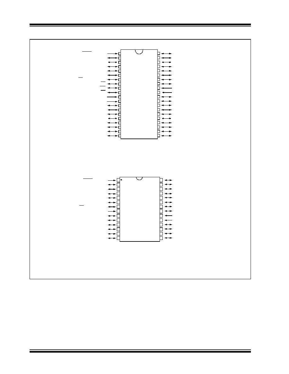
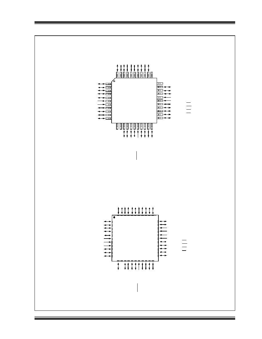
Pin Diagrams
RB7/KBI3/PGD
RB6/KBI2/PGC
RB5/KBI1/PGM
RB4/AN11/KBI0
RB3/AN9/CCP2*
RB2/AN8/INT2
RB1/AN10/INT1
RB0/AN12/INT0
V
DD
V
SS
RD7/PSP7/P1D
RD6/PSP6/P1C
RD5/PSP5/P1B
RD4/PSP4
RC7/RX/DT
RC6/TX/CK
RC5/SDO
RC4/SDI/SDA
RD3/PSP3
RD2/PSP2
MCLR/V
PP
/RE3
RA0/AN0
RA1/AN1
RA2/AN2/V
REF
-/CV
REF
RA3/AN3/V
REF
+
RA4/T0CKI/C1OUT
RA5/AN4/SS/LVDIN/C2OUT
RE0/AN5/RD
RE1/AN6/WR
RE2/AN7/CS
V
DD
V
SS
OSC1/CLKI/RA7
OSC2/CLKO/RA6
RC0/T1OSO/T1CKI
RC1/T1OSI/CCP2*
RC2/CCP1/P1A
RC3/SCK/SCL
RD0/PSP0
RD1/PSP1
1
2
3
4
5
6
7
8
9
10
11
12
13
14
15
16
17
18
19
20
40
39
38
37
36
35
34
33
32
31
30
29
28
27
26
25
24
23
22
21
PIC
18F
43
20
PIC
18F
23
20
10
11
2
3
4
5
6
1
8
7
9
12
13
14
15
16
17
18
19
20
23
24
25
26
27
28
22
21
MCLR/V
PP
/RE3
RA0/AN0
RA1/AN1
RA2/AN2/V
REF
-/CV
REF
RA3/AN3/V
REF
+
RA4/T0CKI/C1OUT
RA5/AN4/SS/LVDIN/C2OUT
V
SS
OSC1/CLKI/RA7
OSC2/CLKO/RA6
RC0/T1OSO/T1CKI
RC1/T1OSI/CCP2
*
RC2/CCP1/P1A
RC3/SCK/SCL
RB7/KBI3/PGD
RB6//KBI2/PGC
RB5/KBI1/PGM
RB4/AN11/KBI0
RB3/AN9/CCP2
*
RB2/AN8/INT2
RB1/AN10/INT1
RB0/AN12/INT0
V
DD
V
SS
RC7/RX/DT
RC6/TX/CK
RC5/SDO
RC4/SDI/SDA
PDIP
SPDIP, SOIC
Note: Pin compatible with 40-pin PIC16C7X devices.
PIC
18F
42
20
PIC
18F
22
20
* RB3 is the alternate pin for the CCP2 pin multiplexing.
2003 Microchip Technology Inc.
DS39599C-page 3
PIC18F2220/2320/4220/4320
Pin Diagrams (Cont.'d)
10
11
2
3
4
5
6
1
18
19
20
21
22
12
13
14
15
38
8
7
44
43
42
41
40
39
16
17
29
30
31
32
33
23
24
25
26
27
28
36
34
35
9
PIC18F4220
37
RA3
/
AN3
/
V
RE
F
+
R
A
2/A
N
2/V
RE
F
-/
C
V
RE
F
RA1
/
A
N
1
RA0
/
A
N
0
MC
L
R
/V
PP
/R
E
3
NC
R
B
7/K
B
I
3/
P
G
D
R
B
6/K
B
I
2/
P
G
C
RB
5/
K
B
I
1
/P
GM
RB
4
/
AN1
1
/
K
BI
0
NC
RC6
/T
X
/
CK
RC5
/SDO
RC4
/SDI/SDA
RD3
/PSP
3
RD2
/PSP
2
RD1
/PSP
1
RD0
/PSP
0
RC3
/SCK/SCL
RC2
/CCP1
/
P1
A
RC1
/T
1
O
SI/CCP
2
*
NC
NC
RC0/T1OSO/T1CKI
OSC2/CLKO/RA6
OSC1/CLKI/RA7
V
SS
V
DD
RE2/AN7/CS
RE1/AN6/WR
RE0/AN5/RD
RA5/AN4/SS/LVDIN/C2OUT
RA4/T0CKI/C1OUT
RC7/RX/DT
RD4/PSP4
RD5/PSP5/P1B
RD6/PSP6/P1C
RD7/PSP7/P1D
V
SS
V
DD
RB0/AN12/INT0
RB1/AN10/INT1
RB2/AN8/INT2
RB3/AN9/CCP2*
TQFP
*
RB3 is the alternate pin for the CCP2 pin multiplexing.
PIC18F4320
10
11
2
3
4
5
6
1
18
19
20
21
22
12
13
14
15
38
8
7
44
43
42
41
40
39
16
17
29
30
31
32
33
23
24
25
26
27
28
36
34
35
9
PIC18F4220
37
RA3
/
A
N
3
/
V
RE
F
+
R
A
2/A
N
2/V
RE
F
-/
C
V
RE
F
RA1
/
A
N
1
RA0
/
A
N
0
MC
L
R
/V
PP
/R
E
3
RB3
/
AN9
/
CCP2
*
RB7
/
KBI
3
/
PG
D
RB6
/
KBI
2
/
PG
C
RB
5
/
K
B
I
1
/P
GM
RB
4
/
AN1
1
/
K
BI
0
NC
RC6
/T
X/CK
RC5
/SDO
RC4
/SDI/
S
DA
RD3
/
PSP3
RD2
/
PSP2
RD1
/
PSP1
RD0
/
PSP0
RC3
/SCK/SCL
RC2
/CCP1
/
P1
A
RC1
/T
1
O
S
I
/CCP2
*
RC
0
/
T
1
OS
O/T
1CK
I
OSC2/CLKO/RA6
OSC1/CLKI/RA7
V
SS
V
SS
V
DD
NC
RE2/AN7/CS
RE1/AN6/WR
RE0/AN5/RD
RA5/AN4/SS/LVDIN/C2OUT
RA4/T0CKI/C1OUT
RC7/RX/DT
RD4/PSP4
RD5/PSP5/P1B
RD6/PSP6/P1C
RD7/PSP7/P1D
V
SS
V
DD
V
DD
RB0/AN12/INT0
RB1/AN10/INT1
RB2/AN8/INT2
QFN
PIC18F4320
*
RB3 is the alternate pin for the CCP2 pin multiplexing.