
TC1044S
TC1044S-12 9/16/96
EVALUATION
KIT
AVAILABLE
© 2001 Microchip Technology Inc. DS21348A
Charge Pump DC-TO-DC Voltage Converter
FEATURES
s
Converts +5V Logic Supply to
±
5V System
s
Wide Input Voltage Range .................... 1.5V to 12V
s
Efficient Voltage Conversion ......................... 99.9%
s
Excellent Power Efficiency ............................... 98%
s
Low Power Consumption ............ 80
µ
A @ V
IN
= 5V
s
Low Cost and Easy to Use
-- Only Two External Capacitors Required
s
RS-232 Negative Power Supply
s
Available in 8-Pin Small Outline (SOIC) and 8-Pin
Plastic DIP Packages
s
Improved ESD Protection ..................... Up to 10kV
s
No External Diode Required for High Voltage
Operation
s
Frequency Boost Raises F
OSC
to 45kHz
GENERAL DESCRIPTION
The TC1044S is a pin-compatible upgrade to the Indus-
try standard TC7660 charge pump voltage converter. It
converts a +1.5V to +12V input to a corresponding ≠1.5V
to ≠12V output using only two low cost capacitors, eliminat-
ing inductors and their associated cost, size and EMI.
Added features include an extended supply range to 12V,
and a frequency boost pin for higher operating frequency,
allowing the use of smaller external capacitors.
The on-board oscillator operates at a nominal frequency
of 10kHz. Frequency is increased to 45kHz when pin 1 is
connected to V
+
. Operation below 10kHz (for lower supply
current applications) is possible by connecting an external
capacitor from OSC to ground (with pin 1 open).
The TC1044S is available in both 8-pin DIP and
8-pin small outline (SOIC) packages in commercial and
extended temperature ranges.
FUNCTIONAL BLOCK DIAGRAM
TC1044S
GND
INTERNAL
VOLTAGE
REGULATOR
RC
OSCILLATOR
VOLTAGE≠
LEVEL
TRANSLATOR
2
V +
CAP +
8
2
7
6
OSC
LV
3
LOGIC
NETWORK
VOUT
5
CAP ≠
4
1
BOOST
ORDERING INFORMATION
Part No.
Package
Temp. Range
TC1044SCOA
8-Pin SOIC
0
∞
C to +70
∞
C
TC1044SCPA
8-Pin Plastic DIP
0
∞
C to +70
∞
C
TC1044SEOA
8-Pin SOIC
≠ 40
∞
C to +85
∞
C
TC1044SEPA
8-Pin Plastic DIP
≠ 40
∞
C to +85
∞
C
TC1044SIJA
8-Pin CerDIP
≠ 25
∞
C to +85
∞
C
TC1044SMJA
8-Pin CerDIP
≠ 55
∞
C to +125
∞
C
TC7660EV
Charge Pump Family Evaluation Kit
PIN CONFIGURATION (DIP AND SOIC)
1
2
3
4
8
7
6
5
TC1044SCPA
TC1044SEPA
TC1044SIJA
TC1044SMJA
BOOST
CAP +
GND
CAP ≠
VOUT
LOW
VOLTAGE (LV)
OSC
+
V
1
2
3
4
8
7
6
5
TC1044SCOA
TC1044SEOA
BOOST
CAP +
GND
CAP ≠
VOUT
LOW
VOLTAGE (LV)
OSC
+
V

TC1044S-12 9/16/96
TC1044S
Charge Pump DC-TO-DC Voltage Converter
2
© 2001 Microchip Technology Inc. DS21348A
Package Power Dissipation (T
A
70
∞
C) (Note 2)
8-Pin CerDIP .................................................. 800mW
8-Pin Plastic DIP ............................................. 730mW
8-Pin SOIC ..................................................... 470mW
Operating Temperature Range
C Suffix .................................................. 0
∞
C to +70
∞
C
I Suffix ............................................... ≠ 25
∞
C to +85
∞
C
E Suffix ............................................. ≠ 40
∞
C to +85
∞
C
M Suffix ........................................... ≠ 55
∞
C to +125
∞
C
Storage Temperature Range ................ ≠ 65
∞
C to +150
∞
C
ELECTRICAL CHARACTERISTICS:
T
A
= +25
∞
C, V
+
= 5V, C
OSC
= 0, Test Circuit (Figure 1), unless otherwise
indicated.
Symbol
Parameter
Test Conditions
Min
Typ
Max
Unit
I
+
Supply Current
R
L
=
--
80
160
µ
A
0
∞
C < T
A
< +70
∞
C
--
--
180
≠ 40
∞
C < T
A
< +85
∞
C
--
--
180
≠ 55
∞
C < T
A
< +125
∞
C
--
--
200
I
+
Supply Current
0
∞
C < T
A
< +70
∞
C
--
--
300
µ
A
(Boost Pin = V
+
)
≠ 40
∞
C < T
A
< +85
∞
C
--
--
350
≠ 55
∞
C < T
A
< +125
∞
C
--
--
400
V
+
H2
Supply Voltage Range, High
Min
T
A
Max,
3
--
12
V
R
L
= 10 k
, LV Open
V
+
L2
Supply Voltage Range, Low
Min
T
A
Max,
1.5
--
3.5
V
R
L
= 10 k
, LV to GND
R
OUT
Output Source Resistance
I
OUT
= 20mA
--
60
100
I
OUT
= 20mA, 0
∞
C
T
A
+70
∞
C
--
70
120
I
OUT
= 20mA, ≠40
∞
C
T
A
+85
∞
C
--
70
120
I
OUT
= 20mA, ≠55
∞
C
T
A
+125
∞
C
--
105
150
V
+
= 2V, I
OUT
= 3 mA, LV to GND
0
∞
C
T
A
+70
∞
C
--
--
250
≠ 55
∞
C
T
A
+125
∞
C
--
--
400
F
OSC
Oscillator Frequency
Pin 7 open; Pin 1 open or GND
--
10
--
kHz
Boost Pin = V
+
--
45
--
P
EFF
Power Efficiency
R
L
= 5 k
; Boost Pin Open
96
98
--
%
T
MIN
< T
A
< T
MAX
; Boost Pin Open
95
97
--
Boost Pin = V
+
--
88
--
V
OUT
E
FF
Voltage Conversion Efficiency
R
L
=
99
99.9
--
%
Z
OSC
Oscillator Impedance
V
+
= 2V
--
1
--
M
V
+
= 5V
--
100
--
k
NOTES: 1. Connecting any input terminal to voltages greater than V
+
or less than GND may cause destructive latch-up. It is recommended that no
inputs from sources operating from external supplies be applied prior to "power up" of the TC1044S.
2. Derate linearly above 50
∞
C by 5.5mW/
∞
C.
ABSOLUTE MAXIMUM RATINGS*
Supply Voltage ......................................................... +13V
LV, Boost and OSC Inputs
Voltage (Note 1) ......................... ≠ 0.3V to (V
+
+ 0.3V)
for V
+
< 5.5V
(V
+
≠ 5.5V) to (V
+
+ 0.3V)
for V
+
> 5.5V
Current Into LV (Note 1) ...................... 20
µ
A for V
+
> 3.5V
Output Short Duration (V
SUPPLY
5.5V) ......... Continuous
Lead Temperature (Soldering, 10 sec) ................. +300
∞
C
*Static-sensitive device. Unused devices must be stored in conductive material. Protect devices from static discharge and static fields. Stresses above those
listed under "Absolute Maximum Ratings" may cause permanent damage to the device. These are stress ratings only and functional operation of the device
at these or any other conditions above those indicated in the operation sections of the specifications is not implied. Exposure to absolute maximum rating
conditions for extended periods may affect device reliability.
3
TC1044S
Charge Pump DC-TO-DC Voltage Converter
TC1044S-12 9/16/96
© 2001 Microchip Technology Inc. DS21348A
Circuit Description
The TC1044S contains all the necessary circuitry to
implement a voltage inverter, with the exception of two
external capacitors, which may be inexpensive 10
µ
F polar-
ized electrolytic capacitors. Operation is best understood by
considering Figure 2, which shows an idealized voltage
inverter. Capacitor C
1
is charged to a voltage, V
+
, for the half
cycle when switches S
1
and S
3
are closed. (Note: Switches
S
2
and S
4
are open during this half cycle.) During the second
half cycle of operation, switches S
2
and S
4
are closed, with
S
1
and S
3
open, thereby shifting capacitor C
1
negatively by
V
+
volts. Charge is then transferred from C
1
to C
2
, such that
the voltage on C
2
is exactly V
+
, assuming ideal switches and
no load on C
2
.
The four switches in Figure 2 are MOS power switches;
S
1
is a P-channel device, and S
2
, S
3
and S
4
are N-channel
devices. The main difficulty with this approach is that in
integrating the switches, the substrates of S
3
and S
4
must
always remain reverse-biased with respect to their sources,
but not so much as to degrade their ON resistances. In
addition, at circuit start-up, and under output short circuit
conditions (V
OUT
= V
+
), the output voltage must be sensed
and the substrate bias adjusted accordingly. Failure to
accomplish this will result in high power losses and probable
device latch-up.
This problem is eliminated in the TC1044S by a logic
network which senses the output voltage (V
OUT
) together
with the level translators, and switches the substrates of
S
3
and S
4
to the correct level to maintain necessary reverse
bias.
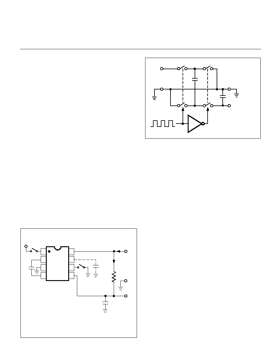
Figure 2. Idealized Charge Pump Inverter
V+
GND
S3
S1
S2
S4
C2
VOUT = ≠ VIN
C1
The voltage regulator portion of the TC1044S is an
integral part of the anti-latch-up circuitry. Its inherent voltage
drop can, however, degrade operation at low voltages. To
improve low-voltage operation, the "LV" pin should be
connected to GND, disabling the regulator. For supply
voltages greater than 3.5V, the LV terminal must be left
open to ensure latch-up-proof operation and prevent device
damage.
Theoretical Power Efficiency
Considerations
In theory, a capacitive charge pump can approach
100% efficiency if certain conditions are met:
(1) The drive circuitry consumes minimal power.
(2) The output switches have extremely low ON
resistance and virtually no offset.
(3) The impedances of the pump and reservoir
capacitors are negligible at the pump frequency.
The TC1044S approaches these conditions for nega-
tive voltage multiplication if large values of C
1
and C
2
are
used. Energy is lost only in the transfer of charge
between capacitors if a change in voltage occurs. The
energy lost is defined by:
E = 1/2 C
1
(V
1
2
≠ V
2
2
)
V
1
and V
2
are the voltages on C
1
during the pump and
transfer cycles. If the impedances of C
1
and C
2
are relatively
high at the pump frequency (refer to Figure 2) compared to
the value of R
L
, there will be a substantial difference in
voltages V
1
and V
2
. Therefore, it is desirable not only to
make C
2
as large as possible to eliminate output voltage
ripple, but also to employ a correspondingly large value for
C
1
in order to achieve maximum efficiency of operation.
1
2
3
4
8
7
6
5
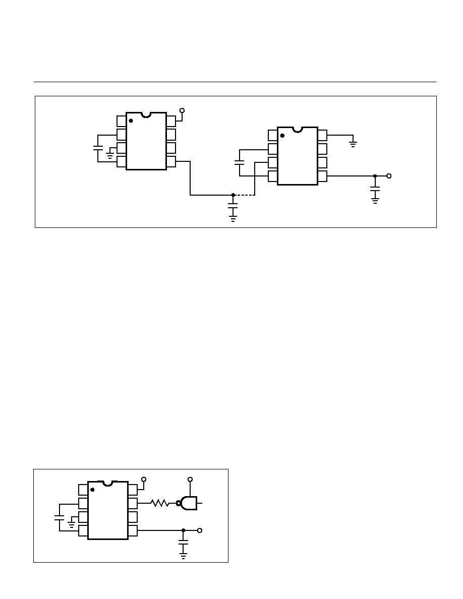
TC1044S
+
V+
(+5V)
VOUT
C1
1
µ
F
COSC
*
+
C2
10
µ
F
IL
RL
IS
V+
NOTE: For large values of C
OSC
(>1000pF), the values
of C
1
and C
2
should be increased to 100
µ
F.
Figure 1. TC1044S Test Circuit

TC1044S-12 9/16/96
TC1044S
Charge Pump DC-TO-DC Voltage Converter
4
© 2001 Microchip Technology Inc. DS21348A
The output characteristics of the circuit in Figure 3 are
those of a nearly ideal voltage source in series with 70
.
Thus, for a load current of ≠10mA and a supply voltage of
+5V, the output voltage would be ≠ 4.3V.
The dynamic output impedance of the TC1044S is due,
primarily, to capacitive reactance of the charge transfer
capacitor (C
1
). Since this capacitor is connected to the
output for only 1/2 of the cycle, the equation is:
Paralleling Devices
Any number of TC1044S voltage converters may be
paralleled to reduce output resistance (Figure 4). The reser-
voir capacitor, C
2
, serves all devices, while each device
requires its own pump capacitor, C
1
. The resultant output
resistance would be approximately:
2
2
f
C
1
X
C
= = 3.18
,
where f = 10 kHz and C
1
= 10
µ
F.
Figure 4. Paralleling Devices Lowers Output Impedance
1
2
3
4
8
7
6
5
TC1044S
V
+
1
2
3
4
8
7
6
5
TC1044S
C1
RL
C2
C1
"n"
"1"
+
Dos and Don'ts
∑ Do not exceed maximum supply voltages.
∑ Do not connect the LV terminal to GND for supply
voltages greater than 3.5V.
∑ Do not short circuit the output to V
+
supply for voltages
above 5.5V for extended periods; however, transient
conditions including start-up are okay.
∑ When using polarized capacitors in the inverting mode,
the + terminal of C
1
must be connected to pin 2 of the
TC1044S and the + terminal of C
2
must be connected
to GND.
Simple Negative Voltage Converter
Figure 3 shows typical connections to provide a nega-
tive supply where a positive supply is available. A similar
scheme may be employed for supply voltages anywhere in
the operating range of +1.5V to +12V, keeping in mind that
pin 6 (LV) is tied to the supply negative (GND) only for supply
voltages below 3.5V.
1
2
3
4
8
7
6
5
TC1044S
10
µ
F
+
V
+
10
µ
F
+
VOUT
*
NOTES:
*
C1
C2
Figure 3. Simple Negative Converter
R
OUT
(of TC1044S)
n (number of devices)
R
OUT
=
5
TC1044S
Charge Pump DC-TO-DC Voltage Converter
TC1044S-12 9/16/96
© 2001 Microchip Technology Inc. DS21348A
Figure 5. Increased Output Voltage by Cascading Devices
situation where the designer has generated the external
clock frequency using TTL logic, the addition of a 10k
pull-
up resistor to V
+
supply is required. Note that the pump
frequency with external clocking, as with internal clocking,
will be 1/2 of the clock frequency. Output transitions occur on
the positive-going edge of the clock.
It is also possible to increase the conversion efficiency
of the TC1044S at low load levels by lowering the oscillator
frequency. This reduces the switching losses, and is achieved
by connecting an additional capacitor, C
OSC
, as shown in
Figure 7. Lowering the oscillator frequency will cause an
undesirable increase in the impedance of the pump (C
1
) and
the reservoir (C
2
) capacitors. To overcome this, increase the
values of C
1
and C
2
by the same factor that the frequency
has been reduced. For example, the addition of a 100pF
capacitor between pin 7 (OSC) and pin 8 (V
+
) will lower the
oscillator frequency to 1kHz from its nominal frequency of
10kHz (a multiple of 10), and necessitate a corresponding
increase in the values of C
1
and C
2
(from 10
µ
F to 100
µ
F).
Positive Voltage Multiplication
The TC1044S may be employed to achieve positive
voltage multiplication using the circuit shown in Figure 8. In
this application, the pump inverter switches of the TC1044S
are used to charge C
1
to a voltage level of V
+
≠ V
F
(where V
+
is the supply voltage and V
F
is the forward voltage drop of
diode D
1
). On the transfer cycle, the voltage on C
1
plus the
supply voltage (V
+
) is applied through diode D
2
to capacitor
C
2
. The voltage thus created on C
2
becomes (2V
+
) ≠ (2V
F
),
or twice the supply voltage minus the combined forward
voltage drops of diodes D
1
and D
2
.
The source impedance of the output (V
OUT
) will depend
on the output current, but for V
+
= 5V and an output current
of 10mA, it will be approximately 60
.
Cascading Devices
The TC1044S may be cascaded as shown (Figure 5) to
produce larger negative multiplication of the initial supply
voltage. However, due to the finite efficiency of each device,
the practical limit is 10 devices for light loads. The output
voltage is defined by:
V
OUT
= ≠n(V
IN
)
where n is an integer representing the number of devices
cascaded. The resulting output resistance would be ap-
proximately the weighted sum of the individual TC1044S
R
OUT
values.
Changing the TC1044S Oscillator Frequency
It may be desirable in some applications (due to noise or
other considerations) to increase the oscillator frequency.
Pin 1, frequency boost pin may be connected to V
+
to
increase oscillator frequency to 45kHz from a nominal of
10kHz for an input supply voltage of 5.0 volts. The oscillator
may also be synchronized to an external clock as shown in
Figure 6. In order to prevent possible device latch-up, a 1k
resistor must be used in series with the clock output. In a
Figure 6. External Clocking
1
2
3
4
8
7
6
5
TC1044S
+
V +
+
CMOS
GATE
10
µ
F
VOUT
10
µ
F
1k
V +
1
2
3
4
8
7
6
5
V
+
1
2
3
4
8
7
6
5
10
µ
F
10
µ
F
"n"
"1"
10
µ
F
VOUT
NOTES:
*
*
+
+
+
TC1044S
TC1044S
1. V
OUT
= ≠n(V
+
) for 1.5V
V
+
12V
10
µ
F
+
TC1044S-12 9/16/96
TC1044S
Charge Pump DC-TO-DC Voltage Converter
6
© 2001 Microchip Technology Inc. DS21348A
Figure 8. Positive Voltage Multiplier
Combined Negative Voltage Conversion
and Positive Supply Multiplication
Figure 9 combines the functions shown in Figures 3 and
8 to provide negative voltage conversion and positive volt-
age multiplication simultaneously. This approach would be,
for example, suitable for generating +9V and ≠5V from an
existing +5V supply. In this instance, capacitors C
1
and C
3
perform the pump and reservoir functions, respectively, for
the generation of the negative voltage, while capacitors C
2
and C
4
are pump and reservoir, respectively, for the multi-
plied positive voltage. There is a penalty in this configuration
which combines both functions, however, in that the source
impedances of the generated supplies will be somewhat
higher due to the finite impedance of the common charge
pump driver at pin 2 of the device.
Efficient Positive Voltage
Multiplication/Conversion
Since the switches that allow the charge pumping op-
eration are bidirectional, the charge transfer can be per-
formed backwards as easily as forwards. Figure 10 shows
a TC1044S transforming ≠5V to +5V (or +5V to +10V, etc.).
The only problem here is that the internal clock and switch-
drive section will not operate until some positive voltage has
been generated. An initial inefficient pump, as shown in
Figure 9, could be used to start this circuit up, after which it
Figure 7. Lowering Oscillator Frequency
1
2
3
4
8
7
6
5
+
V
+
VOUT
C1
COSC
+
C2
TC1044S
will bypass the other (D
1
and D
2
in Figure 9 would never turn
on), or else the diode and resistor shown dotted in Figure 10
can be used to "force" the internal regulator on.
Voltage Splitting
The same bidirectional characteristics used in Figure 10
can also be used to split a higher supply in half, as shown in
Figure 11. The combined load will be evenly shared be-
tween the two sides. Once again, a high value resistor to the
LV pin ensures start-up. Because the switches share the
load in parallel, the output impedance is much lower than in
the standard circuits, and higher currents can be drawn from
the device. By using this circuit, and then the circuit of Figure
5, +15V can be converted (via +7.5V and ≠7.5V) to a nominal
≠15V, though with rather high series resistance (~250
).
1
2
3
4
8
7
6
5
V+
VOUT =
(2 V+) ≠ (2 VF)
+
C2
D1
D2
+
C1
TC1044S
1
2
3
4
8
7
6
5
+
V +
VOUT =
(2 V +) ≠ (2 VF)
C1
D1
+
+
C3
C4
VOUT = ≠V
+
C2
TC1044S
D2
+
Figure 9. Combined Negative Converter and Positive Multiplier
Negative Voltage Generation for
Display ADCs
The TC7106 is designed to work from a 9V battery. With
a fixed power supply system, the TC7106 will perform
conversions with input signal referenced to power supply
ground.
Negative Supply Generation for 4
π/
Digit
Data Acquisition System
The TC7135 is a 4
π/
digit ADC operating from
±
5V
supplies. The TC1044S provides an inexpensive ≠5V source.
(See AN16 and AN17 for TC7135 interface details and
software routines.)
7
TC1044S
Charge Pump DC-TO-DC Voltage Converter
TC1044S-12 9/16/96
© 2001 Microchip Technology Inc. DS21348A
Figure 10. Positive Voltage Conversion
1
2
3
4
8
7
6
5
+
VOUT = ≠V
≠
10
µ
F
+
1 M
V≠ INPUT
C1
10
µ
F
TC1044S
Figure 11. Splitting a Supply in Half
+
+
RL1
RL2
VOUT =
V + ≠V ≠
2
50
µ
F
100
k
100
k
50
µ
F
V +
V ≠
50
µ
F
+
1 M
1
2
8
7
TC1044S
3
4
6
5
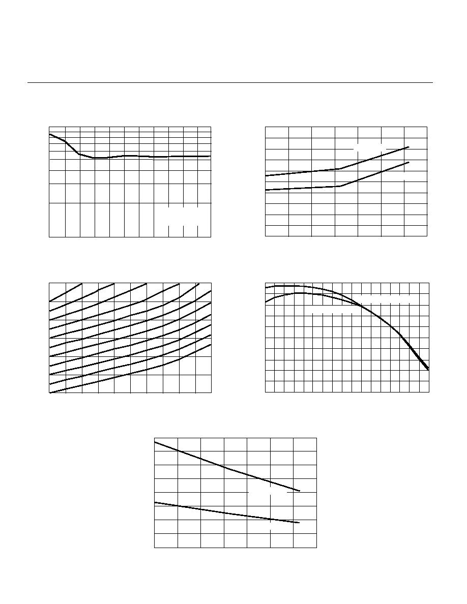
TYPICAL CHARACTERISTICS
Unloaded Osc Freq vs. Temperature
12
10
0
2
4
6
8
-40
-20
0
20
40
100
60
80
OSCILLATOR FREQUENCY (kHz)
TEMPERATURE (
∞
C)
V
IN
= 12V
V
IN
= 5V
Unloaded Osc Freq vs. Temperature
with Boost Pin = V
IN
60
50
0
10
20
30
40
-40
-20
0
20
40
100
60
80
OSCILLATOR FREQUENCY (kHz)
TEMPERATURE (
∞
C)
V
IN
= 12V
V
IN
= 5V
Supply Current vs. Temperature
(with Boost Pin = V
IN
)
1000
0
200
400
600
800
-40
-20
0
20
40
100
60
80
I
DD
(
µ
A)
TEMPERATURE (
∞
C)
V
IN
= 12V
Without Load
10K Load
Voltage Conversion
101.0
100.5
100.0
99.5
99.0
98.5
98.0
1
12
11
10
9
8
7
5
6
4
2
3
VOLTAGE CONVERSION EFFICIENCY (%)
INPUT VOLTAGE V
IN
(V)
T
A
= 25
∞
C
V
IN
= 5V
TC1044S-12 9/16/96
TC1044S
Charge Pump DC-TO-DC Voltage Converter
8
© 2001 Microchip Technology Inc. DS21348A
TYPICAL CHARACTERISTICS (Cont.)
Output Voltage vs. Output Current
0
-2
-4
-6
-8
-10
-12
OUTPUT VOLTAGE V
OUT
(V)
OUTPUT CURRENT (mA)
0
100
90
80
70
60
40
50
30
10
20
1.5
12
11.5
10.5
9.5
8.5
7.5
5.5 6.5
4.5
2.5 3.5
Output Source Resistance vs. Supply Voltage
100
10
30
50
70
OUTPUT SOURCE RESISTANCE (
)
SUPPLY VOLTAGE (V)
Output Source Resistance vs. Temperature
100
0
20
40
60
80
-40
-20
0
20
40
100
60
80
OUTPUT SOURCE RESISTANCE (
)
TEMPERATURE (
∞
C)
V
IN
= 2.5V
V
IN
= 5.5V
Power Conversion Efficiency vs. Load
POWER EFFICIENCY (%)
LOAD CURRENT (mA)
Boost Pin = Open
Boost Pin = V+
0
10
20
30
40
50
60
70
80
90
100
60.0
55.0
50.0
40.0
35.0
30.0
25.0
20.0
15.0
10.0
9.0
7.5
6.0
4.5
3.0
2.0
1.5
1.0
I
OUT
= 20mA
T
A
= 25
∞
C
Supply Current vs. Temperature
200
150
125
175
100
75
50
25
0
SUPPLY CURRENT I
DD
(
µ
A)
TEMPERATURE (
∞
C)
-40
-20
0
20
40
100
60
80
V
IN
= 12.5V
V
IN
= 5.5V
9
TC1044S
Charge Pump DC-TO-DC Voltage Converter
TC1044S-12 9/16/96
© 2001 Microchip Technology Inc. DS21348A
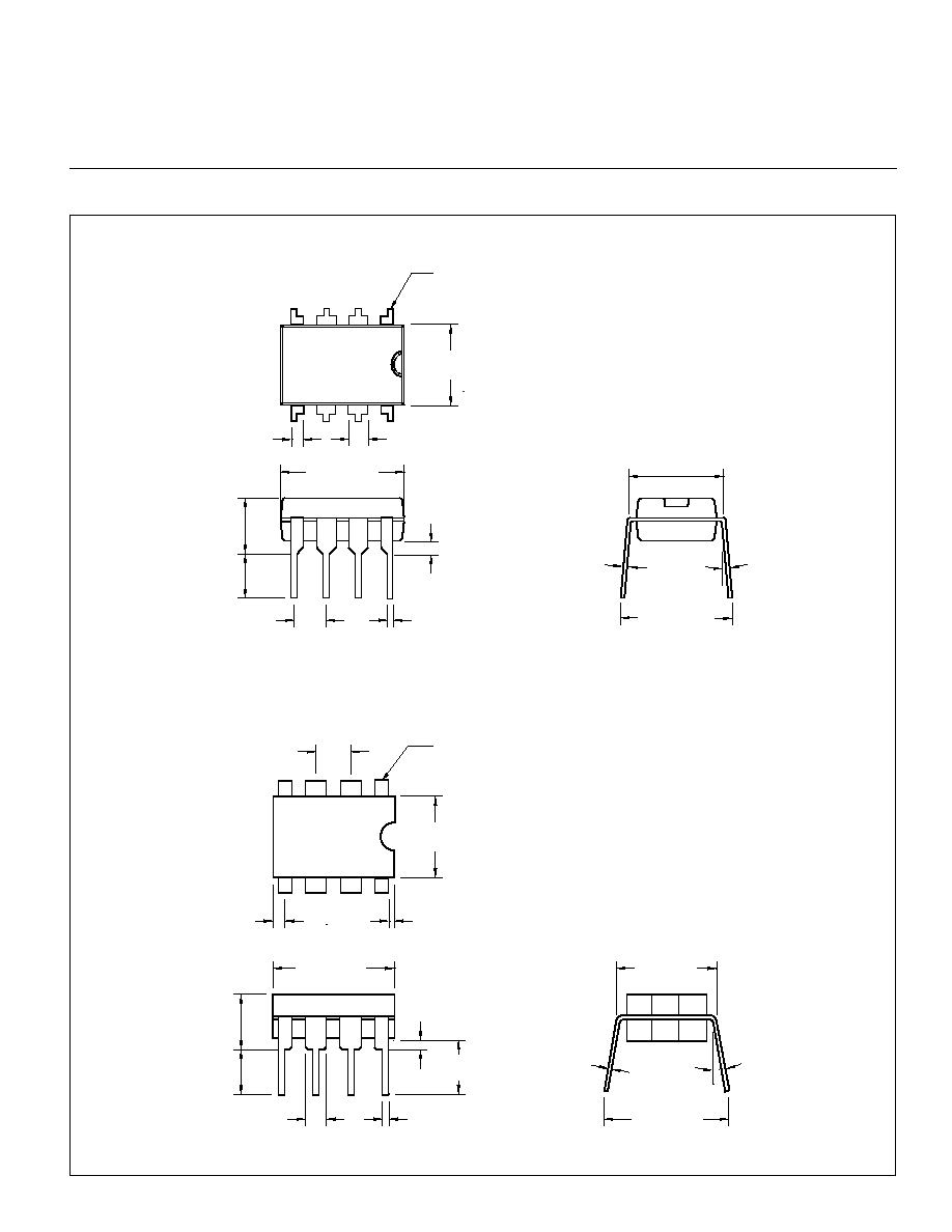
PACKAGE DIMENSIONS
Dimensions: inches (mm)
8-Pin Plastic DIP
3
∞
MIN.
PIN 1
.260 (6.60)
.240 (6.10)
.045 (1.14)
.030 (0.76)
.070 (1.78)
.040 (1.02)
.400 (10.16)
.348 (8.84)
.200 (5.08)
.140 (3.56)
.150 (3.81)
.115 (2.92)
.110 (2.79)
.090 (2.29)
.022 (0.56)
.015 (0.38)
.040 (1.02)
.020 (0.51)
.015 (0.38)
.008 (0.20)
.310 (7.87)
.290 (7.37)
.400 (10.16)
.310 (7.87)
.400 (10.16)
.370 (9.40)
.300 (7.62)
.230 (5.84)
.065 (1.65)
.045 (1.14)
.055 (1.40) MAX.
.020 (0.51) MIN.
PIN 1
.200 (5.08)
.160 (4.06)
.200 (5.08)
.125 (3.18)
.110 (2.79)
.090 (2.29)
.020 (0.51)
.016 (0.41)
.040 (1.02)
.020 (0.51)
.320 (8.13)
.290 (7.37)
.150 (3.81)
MIN.
3
∞
MIN.
.015 (0.38)
.008 (0.20)
.400 (10.16)
.320 (8.13)
8-Pin CerDIP
TC1044S-12 9/16/96
TC1044S
Charge Pump DC-TO-DC Voltage Converter
10
© 2001 Microchip Technology Inc. DS21348A
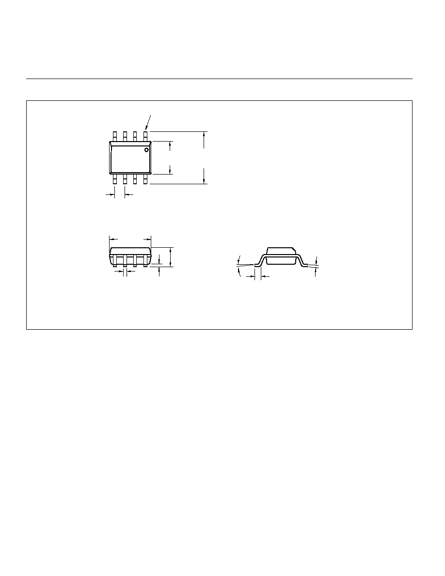
8-Pin SOIC
.050 (1.27) TYP.
8
∞
MAX.
.244 (6.20)
.228 (5.79)
.157 (3.99)
.150 (3.81)
.197 (5.00)
.189 (4.80)
.020 (0.51)
.013 (0.33)
.010 (0.25)
.004 (0.10)
.069 (1.75)
.053 (1.35)
.010 (0.25)
.007 (0.18)
.050 (1.27)
.016 (0.40)
PACKAGE DIMENSIONS (CONT.)
Dimensions: inches (mm)

11
TC1044S
Charge Pump DC-TO-DC Voltage Converter
TC1044S-12 9/16/96
© 2001 Microchip Technology Inc. DS21348A
Information contained in this publication regarding device applications and the like is intended through suggestion only and may be superseded by
updates. It is your responsibility to ensure that your application meets with your specifications. No representation or warranty is given and no liability is
assumed by Microchip Technology Incorporated with respect to the accuracy or use of such information, or infringement of patents or other intellectual
property rights arising from such use or otherwise. Use of MicrochipÌs products as critical components in life support systems is not authorized except with
express written approval by Microchip. No licenses are conveyed, implicitly or otherwise, except as maybe explicitly expressed herein, under any intellec-
tual property rights. The Microchip logo and name are registered trademarks of Microchip Technology Inc. in the U.S.A. and other countries. All rights
reserved. All other trademarks mentioned herein are the property of their respective companies.
All rights reserved. © 2001 Microchip Technology Incorporated. Printed in the USA. 1/01
Printed on recycled paper.
AMERICAS
Corporate Office
2355 West Chandler Blvd.
Chandler, AZ 85224-6199
Tel: 480-792-7200 Fax: 480-792-7277
Technical Support: 480-792-7627
Web Address: http://www.microchip.com
Rocky Mountain
2355 West Chandler Blvd.
Chandler, AZ 85224-6199
Tel: 480-792-7966 Fax: 480-792-7456
Atlanta
500 Sugar Mill Road, Suite 200B
Atlanta, GA 30350
Tel: 770-640-0034 Fax: 770-640-0307
Austin
Analog Product Sales
8303 MoPac Expressway North
Suite A-201
Austin, TX 78759
Tel: 512-345-2030 Fax: 512-345-6085
Boston
2 Lan Drive, Suite 120
Westford, MA 01886
Tel: 978-692-3848 Fax: 978-692-3821
Boston
Analog Product Sales
Unit A-8-1 Millbrook Tarry Condominium
97 Lowell Road
Concord, MA 01742
Tel: 978-371-6400 Fax: 978-371-0050
Chicago
333 Pierce Road, Suite 180
Itasca, IL 60143
Tel: 630-285-0071 Fax: 630-285-0075
Dallas
4570 Westgrove Drive, Suite 160
Addison, TX 75001
Tel: 972-818-7423 Fax: 972-818-2924
Dayton
Two Prestige Place, Suite 130
Miamisburg, OH 45342
Tel: 937-291-1654 Fax: 937-291-9175
Detroit
Tri-Atria Office Building
32255 Northwestern Highway, Suite 190
Farmington Hills, MI 48334
Tel: 248-538-2250 Fax: 248-538-2260
Los Angeles
18201 Von Karman, Suite 1090
Irvine, CA 92612
Tel: 949-263-1888 Fax: 949-263-1338
Mountain View
Analog Product Sales
1300 Terra Bella Avenue
Mountain View, CA 94043-1836
Tel: 650-968-9241 Fax: 650-967-1590
New York
150 Motor Parkway, Suite 202
Hauppauge, NY 11788
Tel: 631-273-5305 Fax: 631-273-5335
San Jose
Microchip Technology Inc.
2107 North First Street, Suite 590
San Jose, CA 95131
Tel: 408-436-7950 Fax: 408-436-7955
Toronto
6285 Northam Drive, Suite 108
Mississauga, Ontario L4V 1X5, Canada
Tel: 905-673-0699 Fax: 905-673-6509
ASIA/PACIFIC
China - Beijing
Microchip Technology Beijing Office
Unit 915
New China Hong Kong Manhattan Bldg.
No. 6 Chaoyangmen Beidajie
Beijing, 100027, No. China
Tel: 86-10-85282100 Fax: 86-10-85282104
China - Shanghai
Microchip Technology Shanghai Office
Room 701, Bldg. B
Far East International Plaza
No. 317 Xian Xia Road
Shanghai, 200051
Tel: 86-21-6275-5700 Fax: 86-21-6275-5060
Hong Kong
Microchip Asia Pacific
RM 2101, Tower 2, Metroplaza
223 Hing Fong Road
Kwai Fong, N.T., Hong Kong
Tel: 852-2401-1200 Fax: 852-2401-3431
India
Microchip Technology Inc.
India Liaison Office
Divyasree Chambers
1 Floor, Wing A (A3/A4)
No. 11, OÌShaugnessey Road
Bangalore, 560 025, India
Tel: 91-80-2290061 Fax: 91-80-2290062
Japan
Microchip Technology Intl. Inc.
Benex S-1 6F
3-18-20, Shinyokohama
Kohoku-Ku, Yokohama-shi
Kanagawa, 222-0033, Japan
Tel: 81-45-471- 6166 Fax: 81-45-471-6122
Korea
Microchip Technology Korea
168-1, Youngbo Bldg. 3 Floor
Samsung-Dong, Kangnam-Ku
Seoul, Korea
Tel: 82-2-554-7200 Fax: 82-2-558-5934
ASIA/PACIFIC
(continued)
Singapore
Microchip Technology Singapore Pte Ltd.
200 Middle Road
#07-02 Prime Centre
Singapore, 188980
Tel: 65-334-8870 Fax: 65-334-8850
Taiwan
Microchip Technology Taiwan
11F-3, No. 207
Tung Hua North Road
Taipei, 105, Taiwan
Tel: 886-2-2717-7175 Fax: 886-2-2545-0139
EUROPE
Australia
Microchip Technology Australia Pty Ltd
Suite 22, 41 Rawson Street
Epping 2121, NSW
Australia
Tel: 61-2-9868-6733 Fax: 61-2-9868-6755
Denmark
Microchip Technology Denmark ApS
Regus Business Centre
Lautrup hoj 1-3
Ballerup DK-2750 Denmark
Tel: 45 4420 9895 Fax: 45 4420 9910
France
Arizona Microchip Technology SARL
Parc dÌActivite du Moulin de Massy
43 Rue du Saule Trapu
Batiment A - ler Etage
91300 Massy, France
Tel: 33-1-69-53-63-20 Fax: 33-1-69-30-90-79
Germany
Arizona Microchip Technology GmbH
Gustav-Heinemann Ring 125
D-81739 Munich, Germany
Tel: 49-89-627-144 0 Fax: 49-89-627-144-44
Germany
Analog Product Sales
Lochhamer Strasse 13
D-82152 Martinsried, Germany
Tel: 49-89-895650-0 Fax: 49-89-895650-22
Italy
Arizona Microchip Technology SRL
Centro Direzionale Colleoni
Palazzo Taurus 1 V. Le Colleoni 1
20041 Agrate Brianza
Milan, Italy
Tel: 39-039-65791-1 Fax: 39-039-6899883
United Kingdom
Arizona Microchip Technology Ltd.
505 Eskdale Road
Winnersh Triangle
Wokingham
Berkshire, England RG41 5TU
Tel: 44 118 921 5869 Fax: 44-118 921-5820
01/09/01
W
ORLDWIDE
S
ALES
AND
S
ERVICE