 | –≠–ª–µ–∫—Ç—Ä–æ–Ω–Ω—ã–π –∫–æ–º–ø–æ–Ω–µ–Ω—Ç: TC1121CUA | –°–∫–∞—á–∞—Ç—å:  PDF PDF  ZIP ZIP |
2002 Microchip Technology Inc.
DS21358B-page 1
M
TC1121
Features
∑ Optional High-Frequency Operation Allows Use of
Small Capacitors
∑ Low Operating Current (FC = GND)
- 50
µ
A
∑ High Output Current (100mA)
∑ Converts a 2.4V to 5.5V Input Voltage to a
Corresponding Negative Output Voltage
(Inverter Mode)
∑ Uses Only 2 Capacitors; No Inductors Required
∑ Selectable Oscillator Frequency
- 10kHz to 200kHz
∑ Power-Saving Shutdown Input
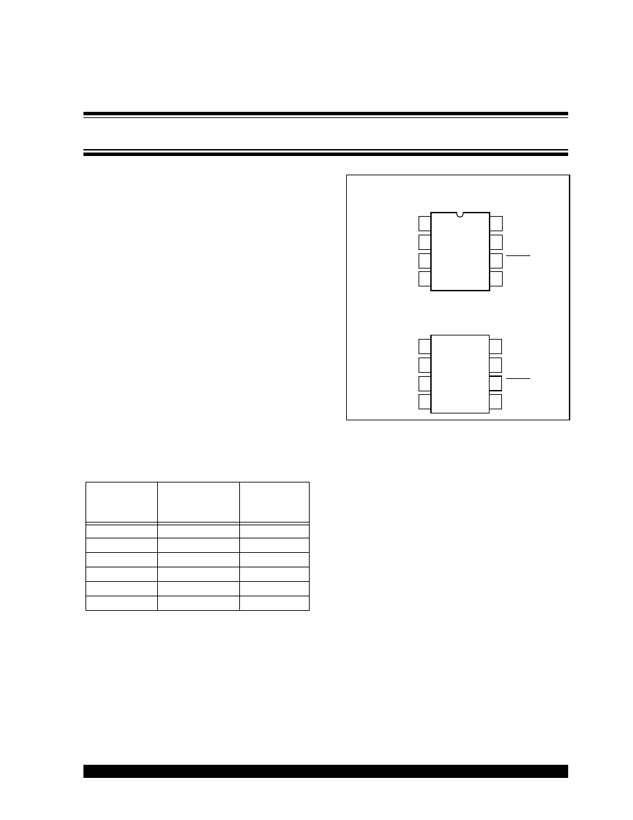
∑ Available in 8-Pin MSOP, 8-Pin PDIP and 8-Pin
Small Outline (SOIC) Packages
Applications
∑ Laptop Computers
∑ Medical Instruments
∑ Disk Drives
∑
µ
P-Based Controllers
∑ Process Instrumentation
Device Selection Table
Package Type
General Description
The TC1121 is a charge pump converter with 100mA
output current capability. It converts a 2.4V to 5.5V
input to a corresponding negative output voltage. As
with all charge pump converters, the TC1121 uses no
inductors saving cost, size and EMI.
An on-board oscillator operates at a typical frequency
of 10kHz (at V
+
= 5V) when the frequency control input
(FC) is connected to ground. The oscillator frequency
increases to 200kHz when FC is connected to V
+
,
allowing the use of smaller capacitors. Operation at
sub-10kHz frequencies results in lower quiescent
NScurrent and is accomplished with the addition of an
external capacitor from OSC (pin 7) to ground. The
TC1121 also can be driven from an external clock
NSconnected OSC. Typical supply current at 10kHz is
50
µ
A, and falls to less than 1
µ
A when the shutdown
input is brought low, whether the internal or an external
clock is used. The TC1121 is available in 8-pin SOIC,
MSOP and PDIP packages.
Part
Number
Package
Operating
Temp.
Range
TC1121COA
8-Pin SOIC
0∞C to +70∞C
TC1121CPA
8-Pin PDIP
0∞C to +70∞C
TC1121CUA
8-Pin MSOP
0∞C to +70∞C
TC1121EOA
8-Pin SOIC
-40∞C to +85∞C
TC1121EPA
8-Pin PDIP
-40∞C to +85∞C
TC1121EUA
8-Pin MSOP
-40∞C to +85∞C
TC1121COA
TC1121EOA
TC1121CUA
TC1121EUA
SHDN
FC
CAP
+
CAP
≠
1
2
3
4
8
7
6
5
GND
OSC
V+
8-Pin SOIC
8-Pin MSOP
V
OUT
TC1121CPA
TC1121EPA
SHDN
FC
CAP
+
CAP
≠
1
2
3
4
8
7
6
5
GND
OSC
V+
8-Pin PDIP
V
OUT
100mA Charge Pump Voltage Converter with Shutdown

TC1121
DS21358B-page 2
2002 Microchip Technology Inc.
Functional Block Diagram
HDN
C1121
SC
Control
C
SC
ND
UT
witch
atrix
RC
Oscillator
ogic
ircuits
2
AP
1
AP

2002 Microchip Technology Inc.
DS21358B-page 3
TC1121
1.0
ELECTRICAL
CHARACTERISTICS
Absolute Maximum Ratings*
Supply Voltage (V
DD
) ............................................... 6V
OSC, FC, SHDN Input Voltage ..... -0.3V to (V
+
+ 0.3V)
Output Short Circuit Duration ........................... 10 Sec.
Package Power Dissipation (T
A
70∞C)
8-Pin PDIP ............................................... 730mW
8-Pin SOIC ............................................... 470mW
8-Pin MSOP ............................................. 333mW
Operating Temperature Range
C Suffix............................................ 0∞C to +70∞C
E Suffix......................................... -40∞C to +85∞C
Storage Temperature Range .............. -65∞C to +150∞C
*Stresses above those listed under "Absolute Maximum
Ratings" may cause permanent damage to the device. These
are stress ratings only and functional operation of the device
at these or any other conditions above those indicated in the
operation sections of the specifications is not implied.
Exposure to Absolute Maximum Rating conditions for
extended periods may affect device reliability.
TC1121 ELECTRICAL SPECIFICATIONS
Electrical Characteristics: T
A
= 0∞C to 70∞C (C suffix), -40∞C to +85∞C (E suffix), V
+
= 5V ±10% C
OSC
= Open, C1, C2 = 10
µ
F,
FC = V
+
, SHDN = V
IH
, typical values are at T
A
= 25∞C unless otherwise noted.
Symbol
Parameter
Min
Typ
Max
Units
Test Conditions
I
DD
Active Supply Current
--
--
50
0.6
100
1
µ
A
mA
R
L
= Open, FC = Open or GND
R
L
= Open, FC = V
+
I
SHUTDOWN
Shutdown Supply Current
--
0.2
1.0
µ
A
SHDN = 0V
V
+
Supply Voltage
2.4
--
5.5
V
V
IH
SHDN Input Logic High
V
DD
x 0.8
--
--
V
V
IL
SHDN Input Logic Low
--
--
0.4
V
I
IN
Input Leakage Current
-1
-4
--
--
1
4
µ
A
SHDN, OSC
FC pin
R
OUT
Output Source Resistance
--
12
20
I
OUT
= 60mA
I
OUT
Output Current
60
100
V
OUT
= more negative than -3.75V
F
OSC
Oscillator Frequency
5
100
10
200
--
--
kHz
Pin 7 Open, Pin 1 Open or GND
SHDN = V
IH
, Pin 1 = V
+
P
EFF
Power Efficiency
--
93
94
--
--
97
97
92
--
--
--
%
FC = GND for all
R
L
= 2k between V
+
and V
OUT
R
L
= 1k
between V
OUT
and GND
I
L
= 60mA to GND
V
EFF
Voltage Conversion Efficiency
99
99.9
--
%
R
L
= Open
Note
1:
Connecting any input terminal to voltages greater than V
+
or less than GND may cause destructive latch-up. It is recommended that no
inputs from sources operating from external supplies be applied prior to "power up" of the TC1121.

TC1121
DS21358B-page 4
2002 Microchip Technology Inc.
2.0
PIN DESCRIPTIONS
The descriptions of the pins are listed in Table 2-1.
TABLE 2-1:
PIN FUNCTION TABLE
Pin No.
(8-Pin MSOP,
PDIP, SOIC)
Symbol
Description
1
FC
Frequency control for internal oscillator, FC = open, F
OSC
= 10kHz typ; FC = V
+
, F
OSC
= 200kHz
typ; FC has no effect when OSC pin is driven externally.
2
CAP
+
Charge-pump capacitor, positive terminal.
3
GND
Power-supply ground input.
4
CAP
≠
Charge-pump capacitor, negative terminal.
5
OUT
Output, negative voltage.
6
SHDN
Shutdown.
7
OSC
Oscillator control input. An external capacitor can be added to slow the oscillator. Take care to
minimize stray capacitance. An external oscillator also may be connected to overdrive OSC.
8
V
+
Power-supply positive voltage input.

2002 Microchip Technology Inc.
DS21358B-page 5
TC1121
3.0
APPLICATIONS
3.1
Negative Voltage Converter
The TC1121 is typically used as a charge-pump voltage
inverter. C1 and C2 are the only two external capacitors
used in the operating circuit (Figure 3-1).
FIGURE 3-1:
CHARGE PUMP
INVERTER
The TC1121 is not sensitive to load current changes,
although its output is not actively regulated. A typical
output source resistance of 11.8
means that an input
of +5V results in -5V output voltage under light load,
and only decreases to -3.8V typ with a 100mA load.
The supplied output current is from capacitor C2 during
one-half the charge-pump cycle. This results in a
peak-to-peak ripple of:
V
RIPPLE
= I
OUT
/2(f
PUMP
) (C2) + I
OUT
(ESR
C2
)
Where f
PUMP
is 5kHz (one half the nominal 10kHz
oscillator frequency), and C2 = 150
µ
F with an ESR of
0.2
, ripple is about 90mV with a 100mA load current.
If C2 is raised to 390
µ
F, the ripple drops to 45mV.
3.2
Changing Oscillator Frequency
The TC1121's clock frequency is controlled by four
modes:
TABLE 3-1:
OSCILLATOR FREQUENCY
MODES
The oscillator runs at 10kHz (typical) when FC and
OSC are not connected. The oscillator frequency is
lowered by connecting a capacitor between OSC and
GND, but FC can still multiply the frequency by 20
times in this mode.
An external clock source that swings within 100mV of
V
+
and GND may overdrive OSC in the inverter mode.
OSC can be driven by any CMOS logic output. When
OSC is overdriven, FC has no effect.
Note that the frequency of the signal appearing at
CAP
+
and CAP
≠
is half that of the oscillator. In addition,
by lowering the oscillator frequency, the effective
output resistance of the charge-pump increases. To
compensate for this, the value of the charge-pump
capacitors may be increased.
Because the 5kHz output ripple frequency may be low
enough to interfere with other circuitry, the oscillator
frequency can be increased with the use of the FC pin
or an external oscillator. The output ripple frequency is
half the selected oscillator frequency. Although the
TC1121's quiescent current will increase if the clock
frequency is increased, it allows smaller capacitance
values to be used for C1 and C2.
3.3
Capacitor Selection
In addition to load current, the following factors affect
the TC1121 output voltage drop from its ideal value 1)
output resistance, 2) pump (C1) and reservoir (C2)
capacitor ESRs and 3) C1 and C2 capacitance.
The voltage drop is the load current times the output
resistance. The loss in C2 is the load current times C2's
ESR; C1's loss is larger because it handles currents
greater than the load current during charge-pump
operation. Therefore, the voltage drop due to C1 is
about four times C1's ESR multiplied by the load
current, and a low (or high) ESR capacitor has a
greater impact on performance for C1 than for C2.
In general, as the TC1121's pump frequency increases,
capacitance values needed to maintain comparable
ripple and output resistance diminish proportionately.
1
2
.4V to 5.5V
UT
C1121
ND
SC
AP
AP
C
UT
N
HDN
SHDN should be tied to V
N
if not used.
SHDN*
FC
OSC
Oscillator Frequency
Open
Open
10kHz
FC = V
+
Open
200kHz
Open or
FC = V
+
External Capacitor
See Typical Operating
Characteristics
Open
External Clock
External Clock Frequency

TC1121
DS21358B-page 6
2002 Microchip Technology Inc.
3.4
Cascading Devices
To produce greater negative magnitudes of the initial
supply voltage, the TC1121 may be cascaded (see
Figure 3-2). Resulting output resistance is approxi-
mately equal to the sum of individual TC1121 R
OUT
values. The output voltage (where n is an integer
representing the number of devices cascaded) is
defined by V
OUT
= -n (V
IN
).
3.5
Paralleling Devices
To reduce output resistance, multiple TC1121s may be
paralleled (see Figure 3-3). Each device needs a pump
capacitor C1, but the reservoir capacitor C2 serves all
devices. The value of C2 should be increased by a
factor of n (the number of devices).
FIGURE 3-2:
CASCADING TC1121s TO INCREASE OUTPUT VOLTAGE
FIGURE 3-3:
PARALLELING TC1121s TO REDUCE OUTPUT RESISTANCE
1
1n
8
7
2
N
2n
C1121
C1121
ND
ND
SC
SC
AP
AP
AP
AP
C
C
HDN
UT
UT
N
UT
V
IN
HDN
HDN*
HDN*
SHDN should be tied to V
IN if
ot used.
1"
n"
C1
1n
2
2
N
C1121
C1121
ND
ND
SC
SC
CAP
+
AP
AP
AP
FC
C
HDN
UT
UT
N
HDN
HDN*
HDN*
IN if
not used.
1"
n"
SC
UT
= R
UT
of TC1121)/n(number of devices)

2002 Microchip Technology Inc.
DS21358B-page 7
TC1121
3.6
Combined Positive Supply
Multiplication and Negative
Voltage Conversion
Figure 3-4 shows this dual function circuit, in which
capacitors C1 and C2 perform pump and reservoir
functions to generate negative voltage. Capacitors C3
and C4 are the respective capacitors for multiplied
positive voltage. This particular configuration leads to
higher source impedances of the generated supplies
due to the finite impedance of the common
charge-pump driver.
FIGURE 3-4:
COMBINED POSITIVE MULTIPLER AND NEGATIVE CONVERTER
1
1
2
1, D2 = 1N4148
2
4
3
V
IN
+
UT
= (
2V
IN
)
≠
V
)
≠
(V
FD2
)
C1121
ND
SC
AP
AP
C
HDN
UT
N
HDN*
UT
=
V
IN
≠
SHDN should be tied to V
IN
if
not used.

TC1121
DS21358B-page 8
2002 Microchip Technology Inc.
4.0
PACKAGING INFORMATION
4.1
Package Marking Information
Package marking data not available at this time.
4.2
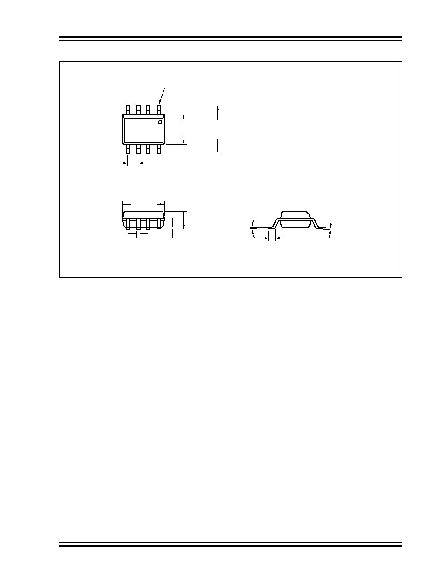
Package Dimensions
8-Pin MSOP
.122 (3.10)
.114 (2.90)
.122 (3.10)
.114 (2.90)
.043 (1.10)
MAX.
.006 (0.15)
.002 (0.05)
.016 (0.40)
.010 (0.25)
.197 (5.00)
.189 (4.80)
.008 (0.20)
.005 (0.13)
.028 (0.70)
.016 (0.40)
6
∞ MAX.
.026 (0.65) TYP.
PIN 1
Dimensions: inches (mm)
3
∞ MIN.
PIN 1
.260 (6.60)
.240 (6.10)
.045 (1.14)
.030 (0.76)
.070 (1.78)
.040 (1.02)
.400 (10.16)
.348 (8.84)
.200 (5.08)
.140 (3.56)
.150 (3.81)
.115 (2.92)
.110 (2.79)
.090 (2.29)
.022 (0.56)
.015 (0.38)
.040 (1.02)
.020 (0.51)
.015 (0.38)
.008 (0.20)
.310 (7.87)
.290 (7.37)
.400 (10.16)
.310 (7.87)
8-Pin Plastic DIP
Dimensions: inches (mm)
2002 Microchip Technology Inc.
DS21358B-page 9
TC1121
Package Dimensions (Continued)
.050 (1.27) TYP.
8
∞
MAX.
PIN 1
.244 (6.20)
.228 (5.79)
.157 (3.99)
.150 (3.81)
.197 (5.00)
.189 (4.80)
.020 (0.51)
.013 (0.33)
.010 (0.25)
.004 (0.10)
.069 (1.75)
.053 (1.35)
.010 (0.25)
.007 (0.18)
.050 (1.27)
.016 (0.40)
.
8-Pin SOIC
Dimensions: inches (mm)

TC1121
DS21358B-page 10
2002 Microchip Technology Inc.
NOTES:

2002 Microchip Technology Inc.
DS21358B-page 11
TC1121
Sales and Support
Data Sheets
Products supported by a preliminary Data Sheet may have an errata sheet describing minor operational differences and recom-
mended workarounds. To determine if an errata sheet exists for a particular device, please contact one of the following:
1.
Your local Microchip sales office
2.
The Microchip Corporate Literature Center U.S. FAX: (480) 792-7277
3.
The Microchip Worldwide Site (www.microchip.com)
Please specify which device, revision of silicon and Data Sheet (include Literature #) you are using.
New Customer Notification System
Register on our web site (www.microchip.com/cn) to receive the most current information on our products.

TC1121
DS21358B-page 12
2002 Microchip Technology Inc.
NOTES:

2002 Microchip Technology Inc.
DS21358B-page 13
TC1121
Information contained in this publication regarding device
applications and the like is intended through suggestion only
and may be superseded by updates. It is your responsibility to
ensure that your application meets with your specifications.
No representation or warranty is given and no liability is
assumed by Microchip Technology Incorporated with respect
to the accuracy or use of such information, or infringement of
patents or other intellectual property rights arising from such
use or otherwise. Use of Microchip's products as critical com-
ponents in life support systems is not authorized except with
express written approval by Microchip. No licenses are con-
veyed, implicitly or otherwise, under any intellectual property
rights.
Trademarks
The Microchip name and logo, the Microchip logo, FilterLab,
K
EE
L
OQ
, microID, MPLAB, PIC, PICmicro, PICMASTER,
PICSTART, PRO MATE, SEEVAL and The Embedded Control
Solutions Company are registered trademarks of Microchip Tech-
nology Incorporated in the U.S.A. and other countries.
dsPIC, ECONOMONITOR, FanSense, FlexROM, fuzzyLAB,
In-Circuit Serial Programming, ICSP, ICEPIC, microPort,
Migratable Memory, MPASM, MPLIB, MPLINK, MPSIM,
MXDEV, PICC, PICDEM, PICDEM.net, rfPIC, Select Mode
and Total Endurance are trademarks of Microchip Technology
Incorporated in the U.S.A.
Serialized Quick Turn Programming (SQTP) is a service mark
of Microchip Technology Incorporated in the U.S.A.
All other trademarks mentioned herein are property of their
respective companies.
© 2002, Microchip Technology Incorporated, Printed in the
U.S.A., All Rights Reserved.
Printed on recycled paper.
Microchip received QS-9000 quality system
certification for its worldwide headquarters,
design and wafer fabrication facilities in
Chandler and Tempe, Arizona in July 1999
and Mountain View, California in March 2002.
The Company's quality system processes and
procedures are QS-9000 compliant for its
PICmicro
Æ
8-bit MCUs, K
EE
L
OQ
Æ
code hopping
devices, Serial EEPROMs, microperipherals,
non-volatile memory and analog products. In
addition, Microchip's quality system for the
design and manufacture of development
systems is ISO 9001 certified.

DS21358B-page 14
2002 Microchip Technology Inc.
M
AMERICAS
Corporate Office
2355 West Chandler Blvd.
Chandler, AZ 85224-6199
Tel: 480-792-7200 Fax: 480-792-7277
Technical Support: 480-792-7627
Web Address: http://www.microchip.com
Rocky Mountain
2355 West Chandler Blvd.
Chandler, AZ 85224-6199
Tel: 480-792-7966 Fax: 480-792-7456
Atlanta
500 Sugar Mill Road, Suite 200B
Atlanta, GA 30350
Tel: 770-640-0034 Fax: 770-640-0307
Boston
2 Lan Drive, Suite 120
Westford, MA 01886
Tel: 978-692-3848 Fax: 978-692-3821
Chicago
333 Pierce Road, Suite 180
Itasca, IL 60143
Tel: 630-285-0071 Fax: 630-285-0075
Dallas
4570 Westgrove Drive, Suite 160
Addison, TX 75001
Tel: 972-818-7423 Fax: 972-818-2924
Detroit
Tri-Atria Office Building
32255 Northwestern Highway, Suite 190
Farmington Hills, MI 48334
Tel: 248-538-2250 Fax: 248-538-2260
Kokomo
2767 S. Albright Road
Kokomo, Indiana 46902
Tel: 765-864-8360 Fax: 765-864-8387
Los Angeles
18201 Von Karman, Suite 1090
Irvine, CA 92612
Tel: 949-263-1888 Fax: 949-263-1338
New York
150 Motor Parkway, Suite 202
Hauppauge, NY 11788
Tel: 631-273-5305 Fax: 631-273-5335
San Jose
Microchip Technology Inc.
2107 North First Street, Suite 590
San Jose, CA 95131
Tel: 408-436-7950 Fax: 408-436-7955
Toronto
6285 Northam Drive, Suite 108
Mississauga, Ontario L4V 1X5, Canada
Tel: 905-673-0699 Fax: 905-673-6509
ASIA/PACIFIC
Australia
Microchip Technology Australia Pty Ltd
Suite 22, 41 Rawson Street
Epping 2121, NSW
Australia
Tel: 61-2-9868-6733 Fax: 61-2-9868-6755
China - Beijing
Microchip Technology Consulting (Shanghai)
Co., Ltd., Beijing Liaison Office
Unit 915
Bei Hai Wan Tai Bldg.
No. 6 Chaoyangmen Beidajie
Beijing, 100027, No. China
Tel: 86-10-85282100 Fax: 86-10-85282104
China - Chengdu
Microchip Technology Consulting (Shanghai)
Co., Ltd., Chengdu Liaison Office
Rm. 2401, 24th Floor,
Ming Xing Financial Tower
No. 88 TIDU Street
Chengdu 610016, China
Tel: 86-28-6766200 Fax: 86-28-6766599
China - Fuzhou
Microchip Technology Consulting (Shanghai)
Co., Ltd., Fuzhou Liaison Office
Unit 28F, World Trade Plaza
No. 71 Wusi Road
Fuzhou 350001, China
Tel: 86-591-7503506 Fax: 86-591-7503521
China - Shanghai
Microchip Technology Consulting (Shanghai)
Co., Ltd.
Room 701, Bldg. B
Far East International Plaza
No. 317 Xian Xia Road
Shanghai, 200051
Tel: 86-21-6275-5700 Fax: 86-21-6275-5060
China - Shenzhen
Microchip Technology Consulting (Shanghai)
Co., Ltd., Shenzhen Liaison Office
Rm. 1315, 13/F, Shenzhen Kerry Centre,
Renminnan Lu
Shenzhen 518001, China
Tel: 86-755-2350361 Fax: 86-755-2366086
Hong Kong
Microchip Technology Hongkong Ltd.
Unit 901-6, Tower 2, Metroplaza
223 Hing Fong Road
Kwai Fong, N.T., Hong Kong
Tel: 852-2401-1200 Fax: 852-2401-3431
India
Microchip Technology Inc.
India Liaison Office
Divyasree Chambers
1 Floor, Wing A (A3/A4)
No. 11, O'Shaugnessey Road
Bangalore, 560 025, India
Tel: 91-80-2290061 Fax: 91-80-2290062
Japan
Microchip Technology Japan K.K.
Benex S-1 6F
3-18-20, Shinyokohama
Kohoku-Ku, Yokohama-shi
Kanagawa, 222-0033, Japan
Tel: 81-45-471- 6166 Fax: 81-45-471-6122
Korea
Microchip Technology Korea
168-1, Youngbo Bldg. 3 Floor
Samsung-Dong, Kangnam-Ku
Seoul, Korea 135-882
Tel: 82-2-554-7200 Fax: 82-2-558-5934
Singapore
Microchip Technology Singapore Pte Ltd.
200 Middle Road
#07-02 Prime Centre
Singapore, 188980
Tel: 65-6334-8870 Fax: 65-6334-8850
Taiwan
Microchip Technology Taiwan
11F-3, No. 207
Tung Hua North Road
Taipei, 105, Taiwan
Tel: 886-2-2717-7175 Fax: 886-2-2545-0139
EUROPE
Denmark
Microchip Technology Nordic ApS
Regus Business Centre
Lautrup hoj 1-3
Ballerup DK-2750 Denmark
Tel: 45 4420 9895 Fax: 45 4420 9910
France
Microchip Technology SARL
Parc d'Activite du Moulin de Massy
43 Rue du Saule Trapu
Batiment A - ler Etage
91300 Massy, France
Tel: 33-1-69-53-63-20 Fax: 33-1-69-30-90-79
Germany
Microchip Technology GmbH
Gustav-Heinemann Ring 125
D-81739 Munich, Germany
Tel: 49-89-627-144 0 Fax: 49-89-627-144-44
Italy
Microchip Technology SRL
Centro Direzionale Colleoni
Palazzo Taurus 1 V. Le Colleoni 1
20041 Agrate Brianza
Milan, Italy
Tel: 39-039-65791-1 Fax: 39-039-6899883
United Kingdom
Arizona Microchip Technology Ltd.
505 Eskdale Road
Winnersh Triangle
Wokingham
Berkshire, England RG41 5TU
Tel: 44 118 921 5869 Fax: 44-118 921-5820
03/01/02
' "% '
W
ORLDWIDE
S
ALES
AND
S
ERVICE