2002 Microchip Technology Inc.
DS21360B-page 1
M
TC1142
Features
∑ Input Range 2.5V to 5.5V
∑ Regulated Output Options from -3.0 to -5.0V
∑ Output Current 20mA (max)
∑ 200kHz Internal Oscillator Frequency
∑ External Synchronizing Clock Input
∑ Logic Level Shutdown
- 1
µ
A (max) Supply Current
∑ Available in 8-Pin MSOP Package
Applications
∑ Cellular Phones
∑ Battery Powered/Portable Equipment
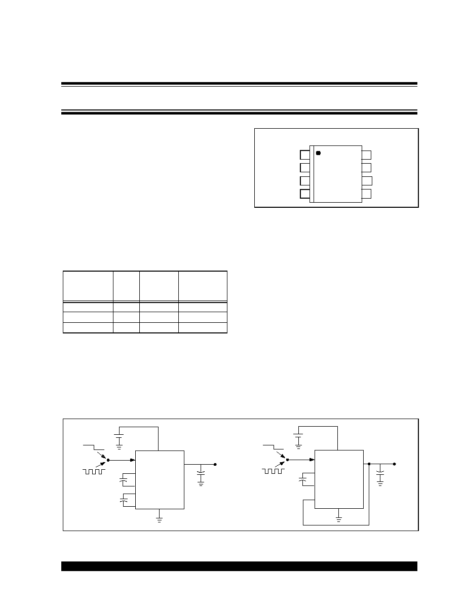
Device Selection Table
*Other output voltages are available (-3.5V and -4.5V). Please
contact Microchip Technology Inc. for details.
Package Type
General Description
The TC1142 generates a regulated negative voltage
from -3V to -5V at 20mA from an input of 2.5V to 5.5V,
using only three external capacitors. Other boost/buck
switching regulators must use an inductor, which is
larger and radiates EMI. An internal voltage
comparator inhibits the charge pump when V
OUT
is
more negative than the regulated value (per the
ordering option). The values of flying capacitors C1 and
C2 are chosen to be less than C
OUT
in order to reduce
the ripple generated from regulating V
OUT
in this
manner. The TC1142 also can be used as a -1x buck
regulator by omitting C2, and connecting the C2 pin to
V
OUT
.
The part goes into shutdown when the CCLK input is
driven low. When in shutdown mode, the part draws a
maximum of 1
µ
A. When CCLK is pulled high, the part
runs from the internal 200kHz oscillator. The device
may be run with an external clock, provided the
frequency is greater than 3kHz and less than 500kHz.
The TC1142 comes in a space-saving MSOP package.
Functional Block Diagram
Part
Number
Output
Voltage
(V)*
Package
Operating
Temp.
Range
TC1142-3.0EUA
3.0
8-Pin MSOP -40∞C to +85∞C
TC1142-4.0EUA
4.0
8-Pin MSOP -40∞C to +85∞C
TC1142-5.0EUA
5.0
8-Pin MSOP -40∞C to +85∞C
GND
C2≠
1
2
3
4
8
7
6
5
TC1142
8-Pin MSOP
C2+
V
OUT
C1≠
V
IN
C1+
CCLK
TC1142-50
CCLK
V
OUT
= -5.0V
GND
V
IN
5.5V to 2.5V
0.47
µF
0.47
µF
C1
C2
4.7
µF
V
OUT
ON
OSC
OVERRIDE
OFF
≠2x Boost/Buck
C
OUT
+
≠
TC1142-30
CCLK
V
OUT
= ≠3.0V
GND
V
IN
5.5V to 3V
0.47
µF
C1
C2≠
4.7
µF
V
OUT
OSC
OVERRIDE
≠1x Buck
C
OUT
ON OFF
+
≠
Inductorless -2x Boost/Buck Regulator

TC1142
DS21360B-page 2
2002 Microchip Technology Inc.
1.0
ELECTRICAL
CHARACTERISTICS
Absolute Maximum Ratings*
Supply Voltage (V
IN
) with C
OUT
Connected ..........6.5V
CCLK Voltage................................-0.3V to (V
+
+ 0.3V)
Power Dissipation.............................................320mW
Operating Temperature Range
8-Pin MSOP ................................. -40∞C to +85∞C
Storage Temperature Range ..............-65∞C to +160∞C
*Stresses above those listed under "Absolute Maximum
Ratings" may cause permanent damage to the device. These
are stress ratings only and functional operation of the device
at these or any other conditions above those indicated in the
operation sections of the specifications is not implied.
Exposure to Absolute Maximum Rating conditions for
extended periods may affect device reliability.
TC1142 ELECTRICAL SPECIFICATIONS
Electrical Characteristics: R
L
=
, V
IN
= 3.2V, Mode = -2x, C1 = C2 = 0.47
µ
F (Note 1), CCLK = V
IH
, C
OUT
= 4.7
µ
F, for V
R
= 3V,
V
IN
= 3.5V, T
A
= T
MIN
to T
MAX
, unless otherwise noted.
Symbol
Parameter
Min
Typ
Max
Units
Test Conditions
V
IN
Supply Voltage
2.5
--
5.5
V
V
OUT
Output Voltage
-(V
R
+ 0.2)
-V
R
-(V
R
≠ 0.2)
V
I
L
= 0mA (Note 2)
V
P-P
Output Ripple
--
100
--
mV
I
L
= 10mA
I
SUPPLY
Supply Current
--
200
400
µ
A
I
SUPPLY1
--
0.1
1
µ
A
CCLK = 0V
R
OUTCL
Closed-Loop Output Resistance
--
2
6
R
OUT
Open-Loop Output Resistance
--
30
--
(Note 3)
f
OSC
Internal Oscillator Frequency
150
200
275
kHz
f
CCLK
External Clock Frequency, Typical
3
--
500
kHz
(Note 4)
P
EFF
Power Efficiency
70
76
--
%
I
L
= 10mA, V
R
= 5V; (See Equation 3-5)
V
IH
CCLK Input High Threshold
2.2
--
--
V
V
IL
CCLK Input Low Threshold
--
--
1.0
V
Note
1:
Assume C1 and C2 have an ESR of 1
.
2:
V
R
is the voltage output specified in the ordering option.
3:
Measured in -1x Mode. For V
R
= 3V, V
IN
= 2.5V.
4:
CCLK is driven with an external clock. Minimum frequency = 1/2t
0
at 50% duty cycle, where t
0
is the counter timeout period.

2002 Microchip Technology Inc.
DS21360B-page 3
TC1142
2.0
PIN DESCRIPTIONS
The descriptions of the pins are listed in Table 2-1.
TABLE 2-1:
PIN FUNCTION TABLE
Pin No.
(8-Pin MSOP)
Symbol
Description
1
V
OUT
Regulated negative output voltage.
2
C2≠
Negative terminal of flying capacitor C2.
3
C2+
Positive terminal of flying capacitor C2.
4
C1≠
Negative terminal of flying capacitor C1.
5
GND
Power supply ground.
6
C1+
Positive terminal of flying capacitor C1.
7
V
IN
Power supply positive voltage input (2.5V to 5.5V).
8
CCLK
Clock control input:
If low, the TC1142 is in Shutdown mode (1
µ
A, max).
If high, the TC1142 runs off the internal oscillator (200kHz, typ.).
CCLK can be overridden by an external oscillator from 3kHz to 500kHz.

TC1142
DS21360B-page 4
2002 Microchip Technology Inc.
3.0
DETAILED DESCRIPTION
The TC1142 inductorless -2x boost/buck regulator is an
inverting charge pump that uses a pulse-frequency
modulation (PFM) control scheme to produce a
regulated negative output voltage, -V
R
, between -3V
and -5V (depending on the output voltage option) at
20mA maximum load. Output voltage regulation is
achieved by gating ON the clock to the charge pump for
a single half-clock period whenever the output is more
positive than V
R
, and gating it OFF when the output is
more negative than -V
R
. The resulting PFM of the clock
applied to the charge pump has a high frequency
spectral content consisting only of clock harmonics.
When using an external clock, the transient noise is
then synchronized to the clock and is easier to filter in
sensitive applications.
The TC1142 also can be used as a -1x boost/buck
regulator by omitting the C2 capacitor and connecting
the C2≠ pin to V
OUT
.
The PFM control scheme minimizes supply current at
small loads and permits the use of low value flying
capacitors, which saves on printed circuit board space
and cost. Due to the TC1142's doubling and inverting
charge pump mechanism, the output voltage is limited
to -2V
IN
. To produce a -5V regulated output, for
example, a minimum input voltage of 2.5V is required
at V
IN
.
The CCLK pin of the TC1142 has three functions: It can
select the internal 200kHz oscillator (when held HIGH),
put the TC1142 into shutdown (when held LOW), or
provide an external clock input. To achieve this
functionality, an internal counter is reset by any positive
transition at the CCLK pin, but will time out in typically
160
µ
sec (i.e., a frequency higher than about 3kHz). If
the counter times out following the last positive
transition, then the internal clock will be gated through
to the charge pump if CCLK is HIGH, or the device will
enter shutdown mode if it is LOW. To enter shutdown,
CCLK must be LOW and the counter must have timed
out. These timing diagrams are shown in Figure 3-4.
A functional circuit diagram of the TC1142 is shown in
Figure 3-1. The output voltage V
OUT
is compared to an
on-chip reference voltage, and the comparator output
is used to gate the charge pump clock. The charge
pump is a negative voltage doubler and has two
phases of operation which are further illustrated in
Figure 3-2 and Figure 3-3. In phase 1, shown in
Figure 3-2, the flying capacitor C1 charges the flying
capacitor C2 while the device load is totally serviced by
the charge stored on the reservoir capacitor C
OUT
. In
phase 2, shown in Figure 3-3, the capacitor C1 is
recharged to V
IN
while the capacitor C2 transfers its
charge to the reservoir capacitor C
OUT
.
In normal operation, the TC1142 charge pump stays in
phase 2 and only switches to phase 1 as required to
maintain output voltage regulation.
FIGURE 3-1:
FUNCTIONAL CIRCUIT DIAGRAM
V
IN
C1+
C1≠
C2+
C2≠
+
C
OUT
V
OUT
+
≠
1.2V
+
Clock
Circuit
OSC
Override
Shutdown
V
IN

2002 Microchip Technology Inc.
DS21360B-page 5
TC1142
FIGURE 3-2:
TC1142 PHASE 1
FIGURE 3-3:
TC1142 PHASE 2
V
IN
C1+
C1+
C2+
C1≠
C2≠
V
IN
C1+
C1≠
C2+
C2≠
+
+
C
OUT
C
OUT
V
OUT
V
OUT
(a)
(b)
(a) Switch positions during phase 1.
(b) The equivalent circuit of the charging phase of operation.
V
IN
V
IN
C1+
C1+
C1≠
C1≠
C2+
C2≠
+
+
C
OUT
C
OUT
V
OUT
V
OUT
(a)
(b)
(a) Switch positions during phase 2.
(b) The equivalent circuit of the discharging phase of operation.
V
IN
V
IN
C2+
C2≠
TC1142
DS21360B-page 6
2002 Microchip Technology Inc.
3.1
Output Voltage and Ripple
For a -2x boost:
In this case, the output voltage is given by:
EQUATION 3-1:
Here, f is the clock frequency and R
S
is the total ON
resistance of the switches connecting C2 to GND and
V
OUT
in phase 2 of the charge pump operating cycle
with the equivalent series resistance (ESR) of C2.
The output ripple voltage is given by:
EQUATION 3-2:
Here, ESR is the equivalent series resistance of C
OUT
.
In this case, the TC1142 is held in phase 2 until the
output voltage drops below V
R
. When this occurs, the
TC1142 reverts to phase 1 for a half period of the clock,
during which C2 is charged from C1. At the end of this
half-period, C2 is reconnected to C
OUT
to boost the
output voltage. During the phase 1 time period, the
output voltage will drop below V
R
before it is boosted
back, so the minimum output voltage is approximated
by:
EQUATION 3-3:
The output ripple voltage is given approximately by:
EQUATION 3-4:
For values of V
IN
higher than |V
R
/2| by several hundred
mV, the effect on ripple of the ESR of C
OUT
can be
neglected compared to the "overdrive" effect of V
IN
.
Here, it can be seen that V
RIPPLE
increases with
increasing V
IN
, but can be minimized by choosing small
C1 and C2 values and a large C
OUT
value.
3.2
Capacitor Selection
To maintain low output impedance and ripple, it is
recommended that capacitors with low equivalent
series resistance (ESR) be used. Additionally, larger
values of the output capacitor and smaller values of the
flying capacitors will reduce output ripple. For a
capacitor value of 4.7
µ
F for C
OUT
, and values of
0.47
µ
F for C1 and C2, the typical output impedance of
the TC1142 in regulation is 0.5
. For the capacitor ESR
not to have a noticeable effect on output impedance, it
should not be larger than 1/2fC
OUT
. This also makes its
effect on ripple voltage negligible. For V
IN
= 3.2V and
V
R
= -5V, the output ripple voltage is less than 70
mV
PP
. Table 3-1 summarizes output ripple versus
capacitor size for an input voltage of 3.2V and a
regulated output voltage of -5V.
Surface mount ceramic capacitors are preferred for
their small size, low cost and low ESR. Low ESR
tantalum capacitors also are acceptable. See Table 3-2
for a list of suggested capacitor suppliers.
TABLE 3-1:
VOLTAGE RIPPLE VS. C1/C2
FLYING CAPACITORS AND
OUTPUT CAPACITOR C
OUT
ESR = 0.1
, I
OUT
= 20mA
a.) For unregulated operation when V
IN
|
|
.
2
V
R
V
OUT
= -|2V
IN
| + I
O
R
OUT
1 1 1 R
S
C2
f C1 C2 (C2 + C
OUT
)
)
(
+
+
where R
OUT
=
V
RIPPLE
= I
O
R
RIPPLE
1 1 ESR C2
2f(C2 + C
OUT)
2fC
OUT
(C2 + C
OUT
)
+
+
where R
RIPPLE
=
b.) For regulated operation when V
IN
>
|
|
.
2
V
R
V
OUT
MIN
= -|V
R
| + I
O
R
OUT
where R
OUT
=
1 ESR C2
2fC
OUT
(C2 + C
OUT
)
+
V
RIPPLE
=
(2
VIN
≠ |V
R
| + ESR I
O
C2 )
N
+
(
)
C1
C2
1 1
1 1
C1 C2
)
(
+
where N =
(C2 + C
OUT
)
C1, C2
(
µ
F)
C
OUT
(
µ
F)
V
IN
(V)
V
OUT
(V)
V
RIPPLE
(mV)
0.1
4.7
3.2
-5
14.6
0.22
4.7
3.2
-5
31.4
0.33
4.7
3.2
-5
46.1
0.47
4.7
3.2
-5
63.9
0.68
4.7
3.2
-5
88.7
1.0
4.7
3.2
-5
123.2
0.1
10
3.2
-5
7.0
0.22
10
3.2
-5
15.1
0.33
10
3.2
-5
22.4
0.47
10
3.2
-5
31.5
0.68
10
3.2
-5
44.7
1.0
10
3.2
-5
63.8

2002 Microchip Technology Inc.
DS21360B-page 7
TC1142
TABLE 3-2:
LOW ESR SURFACE-MOUNT
CAPACITOR
MANUFACTURERS
3.3
Power Efficiency
Assuming the output is loaded with at least 20% of the
maximum available output current, the power efficiency
of the TC1142 can be estimated using the following
equation:
EQUATION 3-5:
For example, a 3.2 Volt V
IN
, and a -5 Volt V
R
will have
an efficiency of approximately 78%. For loads less than
20% of the maximum available output current, the
power efficiency will be substantially reduced. Other
factors that affect the actual efficiency include:
1.
Losses from power consumed by the internal
oscillator (if used).
2.
I
2
R losses due to the on-resistance of the
MOSFET charge pump switches.
3.
Charge pump capacitor losses due to ESR.
4.
Losses that occur during charge transfer (from
the flying capacitors to the output capacitor)
when a voltage difference exists between these
capacitors.
3.4
Choice of -2x or -1x Connections
If required output voltage can be achieved using a -1x
configuration then this is preferred for the following
reasons:
1.
Power efficiency is improved from V
R
/2V
IN
to
V
R
/V
IN
2.
Only one flying capacitor needed
3.
The output ripple becomes proportional to
V
IN
≠ V
R
rather than 2 V
IN
≠ V
R
.
3.5
Layout Considerations
Proper layout is important to obtain optimal perfor-
mance. Mount capacitors as close to their connecting
device pins as possible to minimize stray inductance
and capacitance. It is recommended that a large
ground plane be used to reduce noise leakage into
other circuitry.
FIGURE 3-4:
TIMING DIAGRAM
Manufacturer
Type
Phone
AVX Corp.
TPS series surface-mount
tantalum
X7R type surface-mount
ceramic
803-448-9411
Matsuo
267 series surface-mount
tantalum
X7R type surface-mount
ceramic
714-969-2491
Sprague
593D, 594D, 595D series
surface-mount tantalum
207-324-4140
Murata
Ceramic chip capacitors
800-831-9172
Taiyo Yuden
Ceramic chip capacitors
800-348-2496
Tokin
Ceramic chip capacitors
408-432-8020
= |V
R
|
2(V
IN
)
CCLK
V
OUT
≠V
R
Internal
Oscillator
Shutdown
External
Clock
Shutdown
t
0
= counter timeout (~160
µsec)
t
0
V
IL
GND
V
IH
t
0

TC1142
DS21360B-page 8
2002 Microchip Technology Inc.
4.0
PACKAGING INFORMATION
4.1
Package Marking Information
Package marking data not available at this time.
4.2
Taping Form
4.3
Package Dimensions
Component Taping Orientation for 8-Pin MSOP Devices
Package
Carrier Width (W)
Pitch (P)
Part Per Full Reel
Reel Size
8-Pin MSOP
12 mm
8 mm
2500
13 in
Carrier Tape, Number of Components Per Reel and Reel Size
User Direction of Feed
PIN 1
Standard Reel Component Orientation
for TR Suffix Device
P
8-Pin MSOP
.122 (3.10)
.114 (2.90)
.122 (3.10)
.114 (2.90)
.043 (1.10)
MAX.
.006 (0.15)
.002 (0.05)
.016 (0.40)
.010 (0.25)
.197 (5.00)
.189 (4.80)
.008 (0.20)
.005 (0.13)
.028 (0.70)
.016 (0.40)
6
∞ MAX.
.026 (0.65) TYP.
PIN 1
Dimensions: inches (mm)

2002 Microchip Technology Inc.
DS21360B-page 9
TC1142
Sales and Support
Data Sheets
Products supported by a preliminary Data Sheet may have an errata sheet describing minor operational differences and recom-
mended workarounds. To determine if an errata sheet exists for a particular device, please contact one of the following:
1.
Your local Microchip sales office
2.
The Microchip Corporate Literature Center U.S. FAX: (480) 792-7277
3.
The Microchip Worldwide Site (www.microchip.com)
Please specify which device, revision of silicon and Data Sheet (include Literature #) you are using.
New Customer Notification System
Register on our web site (www.microchip.com/cn) to receive the most current information on our products.

TC1142
DS21360B-page 10
2002 Microchip Technology Inc.
NOTES:

2002 Microchip Technology Inc.
DS21360B-page 11
TC1142
Information contained in this publication regarding device
applications and the like is intended through suggestion only
and may be superseded by updates. It is your responsibility to
ensure that your application meets with your specifications.
No representation or warranty is given and no liability is
assumed by Microchip Technology Incorporated with respect
to the accuracy or use of such information, or infringement of
patents or other intellectual property rights arising from such
use or otherwise. Use of Microchip's products as critical com-
ponents in life support systems is not authorized except with
express written approval by Microchip. No licenses are con-
veyed, implicitly or otherwise, under any intellectual property
rights.
Trademarks
The Microchip name and logo, the Microchip logo, FilterLab,
K
EE
L
OQ
, microID, MPLAB, PIC, PICmicro, PICMASTER,
PICSTART, PRO MATE, SEEVAL and The Embedded Control
Solutions Company are registered trademarks of Microchip Tech-
nology Incorporated in the U.S.A. and other countries.
dsPIC, ECONOMONITOR, FanSense, FlexROM, fuzzyLAB,
In-Circuit Serial Programming, ICSP, ICEPIC, microPort,
Migratable Memory, MPASM, MPLIB, MPLINK, MPSIM,
MXDEV, PICC, PICDEM, PICDEM.net, rfPIC, Select Mode
and Total Endurance are trademarks of Microchip Technology
Incorporated in the U.S.A.
Serialized Quick Turn Programming (SQTP) is a service mark
of Microchip Technology Incorporated in the U.S.A.
All other trademarks mentioned herein are property of their
respective companies.
© 2002, Microchip Technology Incorporated, Printed in the
U.S.A., All Rights Reserved.
Printed on recycled paper.
Microchip received QS-9000 quality system
certification for its worldwide headquarters,
design and wafer fabrication facilities in
Chandler and Tempe, Arizona in July 1999
and Mountain View, California in March 2002.
The Company's quality system processes and
procedures are QS-9000 compliant for its
PICmicro
Æ
8-bit MCUs, K
EE
L
OQ
Æ
code hopping
devices, Serial EEPROMs, microperipherals,
non-volatile memory and analog products. In
addition, Microchip's quality system for the
design and manufacture of development
systems is ISO 9001 certified.

DS21360B-page 12
2002 Microchip Technology Inc.
M
AMERICAS
Corporate Office
2355 West Chandler Blvd.
Chandler, AZ 85224-6199
Tel: 480-792-7200 Fax: 480-792-7277
Technical Support: 480-792-7627
Web Address: http://www.microchip.com
Rocky Mountain
2355 West Chandler Blvd.
Chandler, AZ 85224-6199
Tel: 480-792-7966 Fax: 480-792-7456
Atlanta
500 Sugar Mill Road, Suite 200B
Atlanta, GA 30350
Tel: 770-640-0034 Fax: 770-640-0307
Boston
2 Lan Drive, Suite 120
Westford, MA 01886
Tel: 978-692-3848 Fax: 978-692-3821
Chicago
333 Pierce Road, Suite 180
Itasca, IL 60143
Tel: 630-285-0071 Fax: 630-285-0075
Dallas
4570 Westgrove Drive, Suite 160
Addison, TX 75001
Tel: 972-818-7423 Fax: 972-818-2924
Detroit
Tri-Atria Office Building
32255 Northwestern Highway, Suite 190
Farmington Hills, MI 48334
Tel: 248-538-2250 Fax: 248-538-2260
Kokomo
2767 S. Albright Road
Kokomo, Indiana 46902
Tel: 765-864-8360 Fax: 765-864-8387
Los Angeles
18201 Von Karman, Suite 1090
Irvine, CA 92612
Tel: 949-263-1888 Fax: 949-263-1338
New York
150 Motor Parkway, Suite 202
Hauppauge, NY 11788
Tel: 631-273-5305 Fax: 631-273-5335
San Jose
Microchip Technology Inc.
2107 North First Street, Suite 590
San Jose, CA 95131
Tel: 408-436-7950 Fax: 408-436-7955
Toronto
6285 Northam Drive, Suite 108
Mississauga, Ontario L4V 1X5, Canada
Tel: 905-673-0699 Fax: 905-673-6509
ASIA/PACIFIC
Australia
Microchip Technology Australia Pty Ltd
Suite 22, 41 Rawson Street
Epping 2121, NSW
Australia
Tel: 61-2-9868-6733 Fax: 61-2-9868-6755
China - Beijing
Microchip Technology Consulting (Shanghai)
Co., Ltd., Beijing Liaison Office
Unit 915
Bei Hai Wan Tai Bldg.
No. 6 Chaoyangmen Beidajie
Beijing, 100027, No. China
Tel: 86-10-85282100 Fax: 86-10-85282104
China - Chengdu
Microchip Technology Consulting (Shanghai)
Co., Ltd., Chengdu Liaison Office
Rm. 2401, 24th Floor,
Ming Xing Financial Tower
No. 88 TIDU Street
Chengdu 610016, China
Tel: 86-28-6766200 Fax: 86-28-6766599
China - Fuzhou
Microchip Technology Consulting (Shanghai)
Co., Ltd., Fuzhou Liaison Office
Unit 28F, World Trade Plaza
No. 71 Wusi Road
Fuzhou 350001, China
Tel: 86-591-7503506 Fax: 86-591-7503521
China - Shanghai
Microchip Technology Consulting (Shanghai)
Co., Ltd.
Room 701, Bldg. B
Far East International Plaza
No. 317 Xian Xia Road
Shanghai, 200051
Tel: 86-21-6275-5700 Fax: 86-21-6275-5060
China - Shenzhen
Microchip Technology Consulting (Shanghai)
Co., Ltd., Shenzhen Liaison Office
Rm. 1315, 13/F, Shenzhen Kerry Centre,
Renminnan Lu
Shenzhen 518001, China
Tel: 86-755-2350361 Fax: 86-755-2366086
Hong Kong
Microchip Technology Hongkong Ltd.
Unit 901-6, Tower 2, Metroplaza
223 Hing Fong Road
Kwai Fong, N.T., Hong Kong
Tel: 852-2401-1200 Fax: 852-2401-3431
India
Microchip Technology Inc.
India Liaison Office
Divyasree Chambers
1 Floor, Wing A (A3/A4)
No. 11, O'Shaugnessey Road
Bangalore, 560 025, India
Tel: 91-80-2290061 Fax: 91-80-2290062
Japan
Microchip Technology Japan K.K.
Benex S-1 6F
3-18-20, Shinyokohama
Kohoku-Ku, Yokohama-shi
Kanagawa, 222-0033, Japan
Tel: 81-45-471- 6166 Fax: 81-45-471-6122
Korea
Microchip Technology Korea
168-1, Youngbo Bldg. 3 Floor
Samsung-Dong, Kangnam-Ku
Seoul, Korea 135-882
Tel: 82-2-554-7200 Fax: 82-2-558-5934
Singapore
Microchip Technology Singapore Pte Ltd.
200 Middle Road
#07-02 Prime Centre
Singapore, 188980
Tel: 65-6334-8870 Fax: 65-6334-8850
Taiwan
Microchip Technology Taiwan
11F-3, No. 207
Tung Hua North Road
Taipei, 105, Taiwan
Tel: 886-2-2717-7175 Fax: 886-2-2545-0139
EUROPE
Denmark
Microchip Technology Nordic ApS
Regus Business Centre
Lautrup hoj 1-3
Ballerup DK-2750 Denmark
Tel: 45 4420 9895 Fax: 45 4420 9910
France
Microchip Technology SARL
Parc d'Activite du Moulin de Massy
43 Rue du Saule Trapu
Batiment A - ler Etage
91300 Massy, France
Tel: 33-1-69-53-63-20 Fax: 33-1-69-30-90-79
Germany
Microchip Technology GmbH
Gustav-Heinemann Ring 125
D-81739 Munich, Germany
Tel: 49-89-627-144 0 Fax: 49-89-627-144-44
Italy
Microchip Technology SRL
Centro Direzionale Colleoni
Palazzo Taurus 1 V. Le Colleoni 1
20041 Agrate Brianza
Milan, Italy
Tel: 39-039-65791-1 Fax: 39-039-6899883
United Kingdom
Arizona Microchip Technology Ltd.
505 Eskdale Road
Winnersh Triangle
Wokingham
Berkshire, England RG41 5TU
Tel: 44 118 921 5869 Fax: 44-118 921-5820
03/01/02
' # '
W
ORLDWIDE
S
ALES
AND
S
ERVICE