 | –≠–ª–µ–∫—Ç—Ä–æ–Ω–Ω—ã–π –∫–æ–º–ø–æ–Ω–µ–Ω—Ç: TC1189 | –°–∫–∞—á–∞—Ç—å:  PDF PDF  ZIP ZIP |

2002 Microchip Technology Inc.
DS21364B-page 1
M
TC1188/TC1189
Features
∑ Input Voltage Range: 2.7 V to 6.0 V
∑ 120 mA Output Current
∑ Low Supply Current: 50 µA, (typical)
∑ Low Dropout Voltage: 110 mV, (typical at 100 mA)
∑ Fast Turn-On from Shutdown: 140 µsec (typical)
∑ Low Output Noise
∑ Over-Current and Over-Temperature Protection
∑ Low Power Shutdown Mode
∑ Auto Discharge of Output Capacitor (TC1189)
Applications
∑ Battery Powered Systems
∑ Portable Computers
∑ Medical Instruments
∑ Cellular, Cordless Phones
∑ PDAs
∑ Pagers
Package Type
General Description
The TC1188 and TC1189 are fixed output, low dropout
linear regulators that operate from a 2.7V to 6.0V input
voltage source. The output is capable of delivering up
to 120 mA while consuming only 50 µA of quiescent
current. The low dropout voltage, 120 mV, make the
TC1188 and TC1189 good choices for battery powered
applications. Integrated over-current and over-temper-
ature protection features provide for a fault tolerant
solution.
The TC1189 includes an output voltage auto discharge
feature. When shutdown, the TC1189 will automatically
discharge the output voltage using an internal N-Chan-
nel MOSFET switch.
Fixed output voltage options for the TC1188/TC1189
are: 1.80V, 2.80V, 2.84V and 3.15V. Both the TC1188
and TC1189 are available in SOT23-5 packages.
Typical Application Circuit
GND
SHDN GND
5
1
4
2
3
TC1188
TC1189
5-Pin SOT-23A
NOTE: 5-Pin SOT-23A is equivalent to the EIAJ (SC-74A)
V
IN
V
OUT
V
OUT
V
IN
Output
GND
SHDN
TC1188
TC1189
+
1 µF
≠
C
OUT
GND
Voltage
1 µF
C
IN
Battery
MAX8863/64 Pin Compatible, Low Dropout,
120 mA Linear Regulators

TC1188/TC1189
DS21364B-page 2
2002 Microchip Technology Inc.
1.0
ELECTRICAL
CHARACTERISTICS
Absolute Maximum Ratings*
Input Voltage .........................................................6.5V
Output Short-Circuit Duration .............................Infinite
Output Voltage .......................... (-0.3V) to (V
IN
+ 0.3V)
Maximum Voltage On Any Pin.... (-0.3V) to (V
IN
+0.3V)
Continuous Power Dissipation (T
A
= +70∞C)
SOT-23-5 (derate 7.1 mW/∞C above +70∞C)
..................................................................571 mW
Operating Temperature Range............... -40∞C to 85∞C
Storage Temperature .........................-65∞C to +160∞C
Lead Temperature (Soldering, 10 Sec.) ........... +300∞C
*Notice: *Stresses above those listed under "Absolute
Maximum Ratings" may cause permanent damage to
the device. These are stress ratings only and functional
operation of the device at these or any other conditions
above those indicated in the operation sections of the
specifications is not implied. Exposure to Absolute
Maximum Rating conditions for extended periods may
affect device reliability.
DC SPECIFICATIONS
Electrical Characteristics: V
IN
= +3.6V, GND = 0V, T
A
= T
MIN
to T
MAX
, unless otherwise noted. Typical values are at T
A
= +25∞C.
(Note 1)
Parameters
Symbol
Min
Typ
Max
Units
Conditions
Input Voltage
V
IN
V
OUT
+0.5V
2.7
--
--
6.0
6.0
V
V
OUT
2.5V
V
OUT
= 1.8V (Note 2)
Output Voltage
V
OUT
3.05
3.15
3.25
V
0 mA
I
OUT
50 mA
T
2.75
2.84
2.93
V
0 mA
I
OUT
50 mA
S
2.70
2.80
2.88
V
0 mA
I
OUT
50 mA
R
1.745
1.80
1.85
V
0 mA
I
OUT
50 mA
Q
Maximum Output Current
I
OUT
120
--
--
mA
Current Limit
I
LIM
--
280
--
mA
Note 3
Input Current
I
IN
--
50
90
µA
I
OUT
= 0
Dropout Voltage
--
1.1
--
mV
I
OUT
= 1 mA
--
55
120
mV
I
OUT
= 50 mA
--
110
240
mV
I
OUT
= 100 mA (Note 4)
Line Regulation
V
LNR
-0.10
0.001
0.10
%/V
V
IN
= V
OUT
+
0.5V to 6.0V
--
--
--
%/V
I
OUT
= 1 mA
Load Regulation
V
LDR
--
0.01
0.040
%/mA I
OUT
= 0 mA to 50 mA
Output Voltage Noise
--
350
--
µV
RMS
10 Hz to 1 MHz, C
OUT
= 1 µF
--
220
--
µV
RMS
10 Hz to 1 MHz C
OUT
= 100 µF
Wake Up Time
(from Shutdown Mode)
t
WK
--
10
--
µsec
V
IN
= 3.6V
C
IN
= 1 µF, C
OUT
= 1 µF
I
L
= 30 mA, (See Figure 3-1)
Setting Time
(from Shutdown Mode)
t
S
--
140
--
µsec
V
IN
= 3.6V
C
IN
= 1 µF, C
OUT
= 1 µF
I
L
= 30 mA, (See Figure 3-1)
Note 1: Limits are 100% production tested at T
A
= +25∞C. Limits over the operating temperature range are ensured through cor-
relation using Statistical Quality Control (SQC) methods.
2: Validated by line regulation test.
3: Not tested. For design purposes, the current limit should be considered 150 mA minimum to 410 mA maximum.
4: The dropout voltage is defined as (V
IN
≠ V
OUT
) when V
OUT
is 100 mV below the value of V
OUT
for
V
IN
= V
OUT
+2V.

2002 Microchip Technology Inc.
DS21364B-page 3
TC1188/TC1189
Shutdown:
SHDN Input Threshold
V
IH
2.0
--
--
V
V
IL
--
--
0.4
V
SHDN Input Bias Current
I
shdn
--
0.1
100
nA
V
SHDN
= V
IN
, T
A
= +25∞C, T
A
= T
MAX
--
50
--
nA
V
SHDN
= V
IN
, T
A
= +25∞C, T
A
= T
MAX
Shutdown Supply Current
I
qshdn
--
0.002
1
µ
A
V
OUT
= 0V, T
A
= +25∞C, T
A
= T
MAX
--
0.02
--
µ
A
V
OUT
= 0V, T
A
= +25∞C, T
A
= T
MAX
Shutdown to Output Discharge
Delay (TC1189)
--
1
--
msec
C
OUT
= 1
µ
F, no load at 10% of V
OUT
Thermal Protection
Thermal Shutdown Temperature
T
SHDN
--
170
--
∞C
Thermal Shutdown Hysteresis
T
SHDN
--
20
--
∞C
DC SPECIFICATIONS (CONTINUED)
Electrical Characteristics: V
IN
= +3.6V, GND = 0V, T
A
= T
MIN
to T
MAX
, unless otherwise noted. Typical values are at T
A
= +25∞C.
(Note 1)
Parameters
Symbol
Min
Typ
Max
Units
Conditions
Note 1: Limits are 100% production tested at T
A
= +25∞C. Limits over the operating temperature range are ensured through cor-
relation using Statistical Quality Control (SQC) methods.
2: Validated by line regulation test.
3: Not tested. For design purposes, the current limit should be considered 150 mA minimum to 410 mA maximum.
4: The dropout voltage is defined as (V
IN
≠ V
OUT
) when V
OUT
is 100 mV below the value of V
OUT
for
V
IN
= V
OUT
+2V.

TC1188/TC1189
DS21364B-page 4
2002 Microchip Technology Inc.
2.0
TYPICAL PERFORMANCE CURVES
FIGURE 2-1:
Line Regulation vs.
Temperature. (TC1188)
FIGURE 2-2:
Output Voltage vs.
Temperature. (TC1188)
FIGURE 2-3:
Load Regulation vs.
Temperature. (TC1188)
FIGURE 2-4:
Load Regulation vs.
Temperature. (TC1188)
FIGURE 2-5:
Dropout Voltage vs.
Temperature. (TC1188)
FIGURE 2-6:
Output Noise vs. Frequency.
(TC1188)
Note:
The graphs and tables provided following this note are a statistical summary based on a limited number of
samples and are provided for informational purposes only. The performance characteristics listed herein are
not tested or guaranteed. In some graphs or tables, the data presented may be outside the specified
operating range (e.g., outside specified power supply range) and therefore outside the warranted range.
0.10
0.08
0.06
0.04
0.00
≠0.02
≠0.04
≠0.06
≠0.08
≠0.10
0.02
≠40
∞
C
0
∞
C
25
∞
C
70
∞
C
85
∞
C
TEMPERATURE (
∞
C)
LINE REGULATION (%)
Line Reg. @ 3.50 V
to 5.50V(%)
2.930
2.910
2.890
2.870
2.850
2.830
2.810
2.790
2.770
2.750
≠40
∞
C
0
∞
C
25
∞
C
70
∞
C
85
∞
C
TEMPERATURE (
∞
C)
V
OUT
(V)
V
OUT
- SET/1.0mA
@ 3.5V (V)
0.040
0.035
0.030
0.025
0.020
0.015
0.010
0.005
0.000
≠40
∞
C
0
∞
C
25
∞
C
70
∞
C
85
∞
C
TEMPERATURE (
∞
C)
LOAD REGULATION (%)
Load Reg. 0 to 50mA (%)
0.040
0.035
0.030
0.025
0.020
0.015
0.010
0.005
0.000
≠40
∞
C
0
∞
C
25
∞
C
70
∞
C
85
∞
C
TEMPERATURE (
∞
C)
LOAD REGULATION (%)
Load Reg. 0 to 50mA (%)
Load Reg. 0 to 100mA (%)
0.120
0.100
0.080
0.060
0.040
0.020
0.000
≠40
∞
C
0
∞
C
25
∞
C
70
∞
C
85
∞
C
TEMPERATURE (
∞
C)
(V)
50mA, Dropout V (V)
FREQUENCY (kHz)
Noise (
µ
V/
HZ)
10.0
1.0
0.01
0.01
1
10
100
1000
0.1
0.0
R
LOAD
= 50
µ
C
OUT
= 1
µ
F

2002 Microchip Technology Inc.
DS21364B-page 5
TC1188/TC1189
FIGURE 2-7:
Power Supply Rejection
Ratio vs. Frequency. (TC1188)
FIGURE 2-8:
TC1189 Shutdown Transient
Response.
FIGURE 2-9:
TC1189 Shutdown Transient
Response.
FIGURE 2-10:
TC1189 Line Response.
FIGURE 2-11:
Wake-Up Response Time.
FREQUENCY (kHz)
(dB)
10
100 1K
10K
1M
10M
100K
C
OUT
= 1
µ
F
-10
-20
-30
-40
-60
-70
-50
-80
-90
-100
V
OUT
= 2.84V
R
LOAD
= 50
100mV p-p
CH2 GND
CH1 GND
200
µ
sec/Div
SHDN
SHDN = 0V
V
OUT
= 0.5V/DIV
T = 25
∞
C
IN
= 1
µ
F
C
L
=1
µ
F
R
L
=
CH2 GND
CH1 GND
CH1
CH2
200
µ
sec/Div
C
IN
= 1
µ
F
C
OUT
=1
µ
F
R
L
=
100
V
IN
= 3.5V
T
T
XSHDN = 3V
Turn On
Time = 150
µ
S
No Overshoot
V
OUT
= 2.7V
XSHDN = 0V
V
OUT
= 0V
CH2 GND
CH2
CH1 GND
CH1
100
µ
sec/Div
C
IN
= C
OUT
= 1
µ
F, R
L
= 470
, XSHDN = 3.5V
T
T
V
OUT
AC
20
µ
V/DIV
V
IN
= 4.5V
V
IN
= 3.5V
TIME (100
µ
s/Div)
OUTPUT, SHUTDOWN VOLTAGE (V
)
SHDN
VOUT
0V
2.8V
0V
3V
V
IN
= 3.6V
I
LOAD
= 30mA
C
IN
=
1
µ
F
C
LOAD
= 1
µ
F

TC1188/TC1189
DS21364B-page 6
2002 Microchip Technology Inc.
3.0
PIN DESCRIPTIONS
The descriptions of the pins are listed in Table 3-1.
TABLE 3-1: PIN FUNCTION TABLE
3.1
Detailed Description
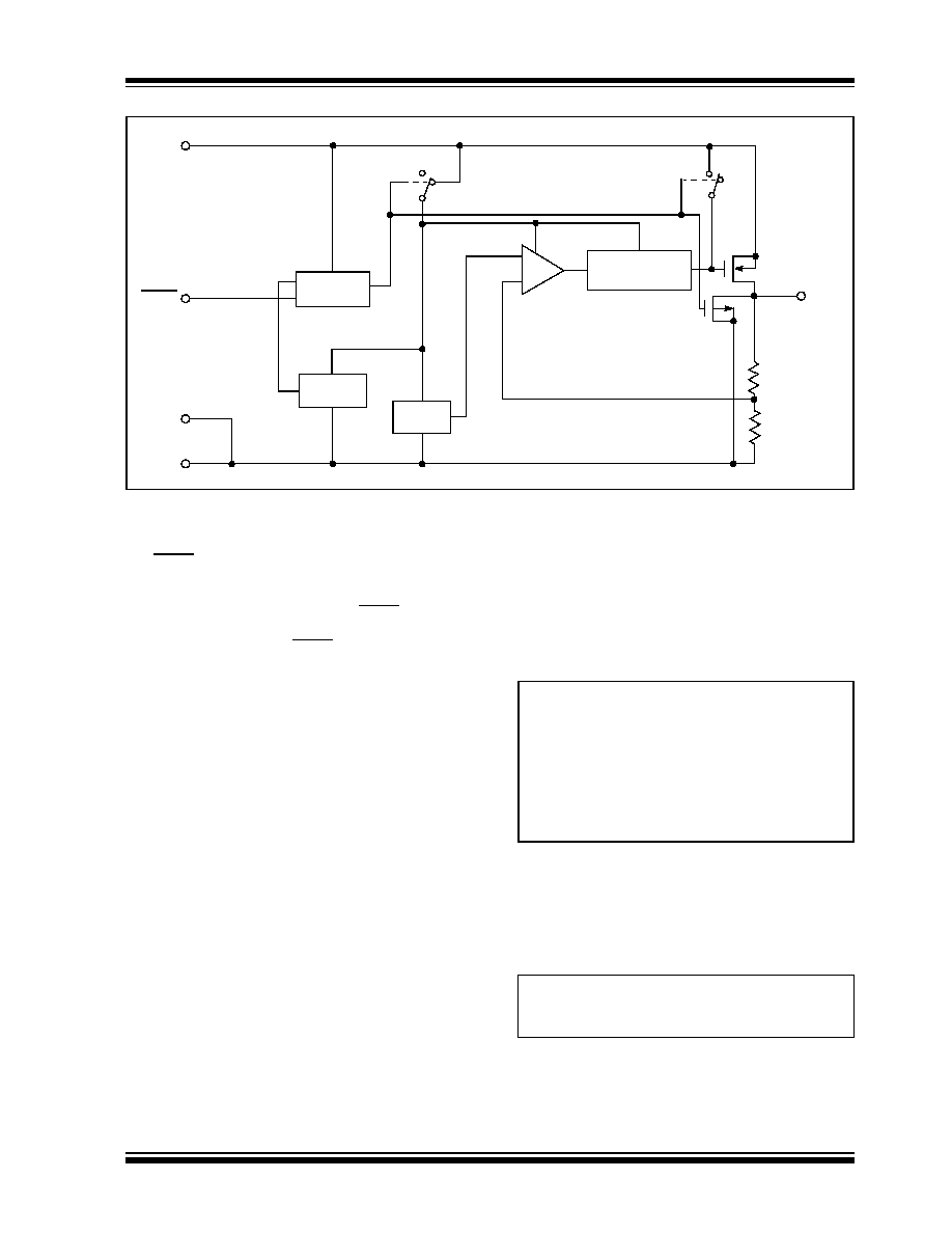
The TC1188/TC1189 devices are fixed output, low
dropout linear regulators. Utilizing CMOS construction,
the internal quiescent current consumed by the regula-
tor is minimized when compared to older bipolar low
dropout regulators.
The LDO output voltage is sensed at the non-inverting
pin of the internal error amplifier. The internal voltage
reference is sensed at the inverting pin of the internal
error amplifier. The error amplifier adjusts the gate
source voltage of the internal P-channel pass device
until the divided down output voltage matches the inter-
nal reference voltage. When it does, the LDO output
voltage is in regulation.
The SHDN, when pulled low, is used to turn off the P-
Channel MOSFET and lower the internal quiescent
current to less than 1 µA maximum. For normal opera-
tion, the SHDN pin is pulled to a high level. (> 2.0V).
The TC1189 incorporates an internal N-Channel MOS-
FET, which is used to discharge the output capacitor
when shutdown. The TC1188 does not have the inter-
nal N-Channel MOSFET, therefore, when the device is
shutdown, the output voltage will decrease at a rate
which is dependant on the load current.
3.2
Turn-On Response
The turn-on response is defined as two separate
response categories: Wake-Up Time (t
WK
) and Settling
Time (t
S
).
The TC1188/TC1189 have fast wake-up times (10 µsec
typical) when released from shutdown. See Figure 3-1
for the wake-up time, designated as t
WK
. The wake-up
time is defined as the time it takes for the output to rise
to 2% of the V
OUT
value after being released from shut-
down.
The total turn on response is defined as the Settling
Time (t
S
) (Figure 3-1). Settling Time (inclusive with t
WK
)
is defined as the condition when the output is within 2%
of its fully enabled value (140 µsec typical) when
released from shutdown. The settling time of the output
voltage is dependent on load conditions and output
capacitance on V
OUT
(RC response).
FIGURE 3-1:
Wake-Up Response Time.
3.3
Internal P-Channel Pass
Transistor
The Internal P-Channel MOSFET is operated in the lin-
ear region to regulate the LDO output voltage. The
RDSon of the P-Channel MOSFET is approximately
1.1
,
making the LDO able to regulate with little input
to output voltage differential, "Low Dropout". Another
benefit of using CMOS construction is that the P-Chan-
nel MOSFET is a voltage controlled device, so it
doesn't consume a fraction of the bias current required
of bipolar PNP LDOs.
Symbol
Description
SHDN
Active Low Shutdown Input. When the SHDN input is low (< 0.2V), the quiscent current for the
TC1188/TC1189 is reduced to 0.1 nA. When the input voltage to the SHDN pin is high (> 2.0V) the
output of the TC1188/TC1189 is enabled. For the TC1189 only, the output capacitor is discharged by
an internal switch when the SHDN is low.
GND
Ground. Connect to ground.
V
IN
Unregulated Input Voltage. The input voltage can range from 2.7V to 6.0V.
V
OUT
Regulator Output. Sources up to 120 mA. Bypass with a 1 µF, <1
typical ESR capacitor to GND.
GND
Connect to GND.
V
IH
t
S
t
WK
V
OUT
98%
2%
V
IL
SHDN
2002 Microchip Technology Inc.
DS21364B-page 7
TC1188/TC1189
FIGURE 3-2:
Functional Block Diagram.
3.4
Shutdown
The SHDN input is used to turn off the LDO P-Channel
pass MOSFET and internal bias. When shutdown, the
typical quiescent current consumed by the LDO is
0.1 nA. A logic low (< 0.4V) at the SHDN input will
cause the device to operate in the shutdown mode. A
logic high (> 2.0V) at the SHDN input will cause the
device to operate in the normal mode.
3.5
Current Limit
The LDO output current is monitored internal to the
TC1188/TC1189. The internal current sense will limit
the LDO output current to a typical value of 280 mA.
The current limit can range from approximately 50 mA
to 410 mA from device to device. The internal current
limit protects the device from a continuous output short
circuit.
3.6
Thermal Overload Protection
Integrated thermal protection circuitry shuts the
TC1188/TC1189 off when the internal die temperature
exceeds approximately 170∞C. The regulator output
remains off until the internal die temperature drops to
approximately 150∞C.
3.7
Operating Region and Power
Dissipation
The internal power dissipation to the LDO is primarily
determined by the input voltage, output voltage and
output current. The following equation is used to
approximate the worst case for power dissipation:
EQUATION
The maximum power dissipation is a function of the
maximum ambient temperature, T
A(MAX)
, the maximum
junction temperature, T
J(MAX)
, and the package thermal
resistance from junction to air,
JA
. The 5-Pin SOT23A
package has a
JA
of approximately 220∞C/Watt.
EQUATION
Bandgap
Reference
MOS Driver
W
ith
I
LIMIT
Thermal
Sensor
Shutdown
Logic
Error
+
≠
V
IN
SHDN
GND
V
OUT
PMOS Pass
GND
N
(TC1189 Only)
Amplifier
Transistor
P
D
= V
IN(MAX)
- V
OUT(MIN)
x I
LOAD(MAX)
Where:
P
D
= Worst case internal power dissipation.
V
IN
(
MAX
)
= Maximum input voltage.
V
OUT
(
MIN
)
= Minimum output voltage.
I
LOAD
(
MAX
)
= Maximum output current.
P
D
= (T
J(MAX)
- T
A(MAX)
)/
JA
Where all terms are previously defined.

TC1188/TC1189
DS21364B-page 8
2002 Microchip Technology Inc.
EXAMPLE 3-1:
The previously defined power dissipation equations
can be used to ensure that the regulator thermal
operation is within limits.
Given:
V
IN(MAX)
= 3.0V +10%
V
OUT(MAX)
= 2.7V - 2.5%
I
LOAD(MAX)
= 40
M
A
T
J(MAX)
= 125∞C
T
A(MAX)
= 55∞C
Find:
1.
Actual power dissipation.
2.
Maximum allowable dissipation.
Actual power dissipation:
Maximum allowable power dissipation:
In this example, the TC1188/TC1189 dissipates a max-
imum of 26.7 mW below the allowable limit of 318 mW.
In a similar manner, the power dissipation equation, as
a function of V
IN
, V
OUT
and I
LOAD,
along with the power
dissipation equation, as a function of maximum junction
temperature, maximum ambient temperature and junc-
tion to air thermal resistance, can be used to calculate
maximum current and/or maximum input voltage limits.
4.0
APPLICATIONS INFORMATION
4.1
Input Capacitor
A 1 µF (or larger) capacitor is recommended to bypass
the LDO input and lower input impedance for circuit
stability when operating from batteries or high imped-
ance sources. The input capacitor can be ceramic, tan-
talum or aluminum electrolytic. For applications that
require low noise and input power supply rejection, low
effective series resistance (ESR) ceramic capacitors
are recommended over higher ESR electrolytic capac-
itors. Larger value input capacitors can be used to
improve circuit performance.
4.2
Output Capacitor
A 1 µF (minimum) capacitor is required from V
OUT
to
ground to ensure circuit stability. The output capacitor
should have an ESR greater than 0.1 ohms and less
than 2 ohm. Tantalum or aluminum electrolytic capaci-
tors are recommended. Since many aluminum electro-
lytic capacitors freeze at approximately -30∞C, solid
tantalums are recommended for applications operating
below 25∞C.
P
D
= V
IN(MAX)
- V
OUT(MIN)
x I
LOAD(MAX)
P
D
= ((3.0 * 1.1) - (2.7 * 0.975)) * 40 mA
P
D
= 26.7 mWatts
P
D
= (T
J(MAX)
- T
A(MAX)
)/
JA
P
D(MAX)
= (125 - 55) / 220
P
D(MAX)
= 318 mWatts.

2002 Microchip Technology Inc.
DS21364B-page 9
TC1188/TC1189
5.0
PACKAGING INFORMATION
5.1
Package Marking Information
2
4
5
3
1
Part Number
(V)
Code
TC1188-XECT
1.80
G4
TC1188-XECT
2.80
G3
TC1188-XECT
2.84
G2
TC1188-XECT
3.15
G1
TC1189-XECT
1.80
H4
TC1189-XECT
2.80
H3
TC1189-XECT
2.84
H2
TC1189-XECT
3.15
H1
Legend: 1-2 Part Number code + temperature range and voltage*
3
Year and two-month period code
4
Lot ID
Note: In the event the full Microchip part number cannot be marked on one line, it will
be carried over to the next line thus limiting the number of available characters
for customer specific information.
*
Standard OTP marking consists of Microchip part number, year code, week code, and traceability code.

TC1188/TC1189
DS21364B-page 10
2002 Microchip Technology Inc.
5-Lead Plastic Small Outline Transistor (OT) (SOT23)
10
5
0
10
5
0
Mold Draft Angle Bottom
10
5
0
10
5
0
Mold Draft Angle Top
0.50
0.43
0.35
.020
.017
.014
B
Lead Width
0.20
0.15
0.09
.008
.006
.004
c
Lead Thickness
10
5
0
10
5
0
Foot Angle
0.55
0.45
0.35
.022
.018
.014
L
Foot Length
3.10
2.95
2.80
.122
.116
.110
D
Overall Length
1.75
1.63
1.50
.069
.064
.059
E1
Molded Package Width
3.00
2.80
2.60
.118
.110
.102
E
Overall Width
0.15
0.08
0.00
.006
.003
.000
A1
Standoff ß
1.30
1.10
0.90
.051
.043
.035
A2
Molded Package Thickness
1.45
1.18
0.90
.057
.046
.035
A
Overall Height
1.90
.075
p1
Outside lead pitch (basic)
0.95
.038
p
Pitch
5
5
n
Number of Pins
MAX
NOM
MIN
MAX
NOM
MIN
Dimension Limits
MILLIMETERS
INCHES*
Units
1
p
D
B
n
E
E1
L
c
A2
A
A1
p1
* Controlling Parameter
Notes:
Dimensions D and E1 do not include mold flash or protrusions. Mold flash or protrusions shall not exceed
.010" (0.254mm) per side.
JEDEC Equivalent: MO-178
Drawing No. C04-091
ß Significant Characteristic

2002 Microchip Technology Inc.
DS21364B-page11
TC1188/TC1189
ON-LINE SUPPORT
Microchip provides on-line support on the Microchip
World Wide Web (WWW) site.
The web site is used by Microchip as a means to make
files and information easily available to customers. To
view the site, the user must have access to the Internet
and a web browser, such as Netscape or Microsoft
Explorer. Files are also available for FTP download
from our FTP site.
Connecting to the Microchip Internet Web Site
The Microchip web site is available by using your
favorite Internet browser to attach to:
www.microchip.com
The file transfer site is available by using an FTP ser-
vice to connect to:
ftp://ftp.microchip.com
The web site and file transfer site provide a variety of
services. Users may download files for the latest
Development Tools, Data Sheets, Application Notes,
User's Guides, Articles and Sample Programs. A vari-
ety of Microchip specific business information is also
available, including listings of Microchip sales offices,
distributors and factory representatives. Other data
available for consideration is:
∑ Latest Microchip Press Releases
∑ Technical Support Section with Frequently Asked
Questions
∑ Design Tips
∑ Device Errata
∑ Job Postings
∑ Microchip Consultant Program Member Listing
∑ Links to other useful web sites related to
Microchip Products
∑ Conferences for products, Development Systems,
technical information and more
∑ Listing of seminars and events
Systems Information and Upgrade Hot Line
The Systems Information and Upgrade Line provides
system users a listing of the latest versions of all of
Microchip's development systems software products.
Plus, this line provides information on how customers
can receive any currently available upgrade kits.The
Hot Line Numbers are:
1-800-755-2345 for U.S. and most of Canada, and
1-480-792-7302 for the rest of the world.
013001

TC1188/TC1189
DS21364B-page12
2002 Microchip Technology Inc.
READER RESPONSE
It is our intention to provide you with the best documentation possible to ensure successful use of your Microchip prod-
uct. If you wish to provide your comments on organization, clarity, subject matter, and ways in which our documentation
can better serve you, please FAX your comments to the Technical Publications Manager at (480) 792-4150.
Please list the following information, and use this outline to provide us with your comments about this Data Sheet.
1. What are the best features of this document?
2. How does this document meet your hardware and software development needs?
3. Do you find the organization of this data sheet easy to follow? If not, why?
4. What additions to the data sheet do you think would enhance the structure and subject?
5. What deletions from the data sheet could be made without affecting the overall usefulness?
6. Is there any incorrect or misleading information (what and where)?
7. How would you improve this document?
8. How would you improve our software, systems, and silicon products?
To:
Technical Publications Manager
RE:
Reader Response
Total Pages Sent
From: Name
Company
Address
City / State / ZIP / Country
Telephone: (_______) _________ - _________
Application (optional):
Would you like a reply? Y N
Device:
Literature Number:
Questions:
FAX: (______) _________ - _________
DS21364B
TC1188/TC1189

2002 Microchip Technology Inc.
DS21364B-page13
TC1188/TC1189
PRODUCT IDENTIFICATION SYSTEM
To order or obtain information, e.g., on pricing or delivery, refer to the factory or the listed sales office.
Sales and Support
Data Sheets
Products supported by a preliminary Data Sheet may have an errata sheet describing minor operational differences and recom-
mended workarounds. To determine if an errata sheet exists for a particular device, please contact one of the following:
1.
Your local Microchip sales office
2.
The Microchip Corporate Literature Center U.S. FAX: (480) 792-7277
3.
The Microchip Worldwide Site (www.microchip.com)
Please specify which device, revision of silicon and Data Sheet (include Literature #) you are using.
New Customer Notification System
Register on our web site (www.microchip.com/cn) to receive the most current information on our products.
PART NO.
X
/XX
Package
Voltage
Output
Device
Device:
TC1188: 100 mA, MAX8863/64 Pin Compatible LDO
TC1189: 100 mA, MAX8863/64 Pin Compatible LDO
Voltage Output
Options:
Q
= 1.80V
R
= 2.80V
S
= 2.84V
T
= 3.15V
Package:
ECTTR
= SOT-23A, 5-Pin (Tape and Reel)
Examples:
a)
TC1188QECTTR: 1.80V,
100 mA,
MAX8863/64 Pin Compatible LDO
b)
TC1188RECTTR: 2.80V,
100 mA,
MAX8863/64 Pin Compatible LDO
c)
TC1188SECTTR: 2.84V,
100 mA,
MAX8863/64 Pin Compatible LDO
d)
TC1188TECTTR: 3.15V,
100 mA,
MAX8863/64 Pin Compatible LDO
a)
TC1189QECTTR: 1.80V,
100 mA,
MAX8863/64 Pin Compatible LDO
b)
TC1189RECTTR: 2.80V,
100 mA,
MAX8863/64 Pin Compatible LDO
c)
TC1189SECTTR: 2.84V,
100 mA,
MAX8863/64 Pin Compatible LDO
d)
TC1189TECTTR: 3.15V,
100 mA,
MAX8863/64 Pin Compatible LDO

TC1188/TC1189
DS21364B-page 14
2002 Microchip Technology Inc.
NOTES:
2002 Microchip Technology Inc.
DS21364B-page 15
TC1188/TC1189
Information contained in this publication regarding device
applications and the like is intended through suggestion only
and may be superseded by updates. It is your responsibility to
ensure that your application meets with your specifications.
No representation or warranty is given and no liability is
assumed by Microchip Technology Incorporated with respect
to the accuracy or use of such information, or infringement of
patents or other intellectual property rights arising from such
use or otherwise. Use of Microchip's products as critical com-
ponents in life support systems is not authorized except with
express written approval by Microchip. No licenses are con-
veyed, implicitly or otherwise, under any intellectual property
rights.
Trademarks
The Microchip name and logo, the Microchip logo, FilterLab,
K
EE
L
OQ
, microID, MPLAB, MXDEV, PIC, PICmicro,
PICMASTER, PICSTART, PRO MATE, SEEVAL and The
Embedded Control Solutions Company are registered trade-
marks of Microchip Technology Incorporated in the U.S.A. and
other countries.
dsPIC, dsPICDEM.net, ECONOMONITOR, FanSense,
FlexROM, fuzzyLAB, In-Circuit Serial Programming, ICSP,
ICEPIC, microPort, Migratable Memory, MPASM, MPLIB,
MPLINK, MPSIM, MXLAB, PICC, PICDEM, PICDEM.net,
rfPIC, Select Mode and Total Endurance are trademarks of
Microchip Technology Incorporated in the U.S.A.
Serialized Quick Turn Programming (SQTP) is a service mark
of Microchip Technology Incorporated in the U.S.A.
All other trademarks mentioned herein are property of their
respective companies.
© 2002, Microchip Technology Incorporated, Printed in the
U.S.A., All Rights Reserved.
Printed on recycled paper.
Microchip received QS-9000 quality system
certification for its worldwide headquarters,
design and wafer fabrication facilities in
Chandler and Tempe, Arizona in July 1999
and Mountain View, California in March 2002.
The Company's quality system processes and
procedures are QS-9000 compliant for its
PICmicro
Æ
8-bit MCUs, K
EE
L
OQ
Æ
code hopping
devices, Serial EEPROMs, microperipherals,
non-volatile memory and analog products. In
addition, Microchip's quality system for the
design and manufacture of development
systems is ISO 9001 certified.

DS21364B-page 16
2002 Microchip Technology Inc.
M
AMERICAS
Corporate Office
2355 West Chandler Blvd.
Chandler, AZ 85224-6199
Tel: 480-792-7200 Fax: 480-792-7277
Technical Support: 480-792-7627
Web Address: http://www.microchip.com
Rocky Mountain
2355 West Chandler Blvd.
Chandler, AZ 85224-6199
Tel: 480-792-7966 Fax: 480-792-4338
Atlanta
500 Sugar Mill Road, Suite 200B
Atlanta, GA 30350
Tel: 770-640-0034 Fax: 770-640-0307
Boston
2 Lan Drive, Suite 120
Westford, MA 01886
Tel: 978-692-3848 Fax: 978-692-3821
Chicago
333 Pierce Road, Suite 180
Itasca, IL 60143
Tel: 630-285-0071 Fax: 630-285-0075
Dallas
4570 Westgrove Drive, Suite 160
Addison, TX 75001
Tel: 972-818-7423 Fax: 972-818-2924
Detroit
Tri-Atria Office Building
32255 Northwestern Highway, Suite 190
Farmington Hills, MI 48334
Tel: 248-538-2250 Fax: 248-538-2260
Kokomo
2767 S. Albright Road
Kokomo, Indiana 46902
Tel: 765-864-8360 Fax: 765-864-8387
Los Angeles
18201 Von Karman, Suite 1090
Irvine, CA 92612
Tel: 949-263-1888 Fax: 949-263-1338
New York
150 Motor Parkway, Suite 202
Hauppauge, NY 11788
Tel: 631-273-5305 Fax: 631-273-5335
San Jose
Microchip Technology Inc.
2107 North First Street, Suite 590
San Jose, CA 95131
Tel: 408-436-7950 Fax: 408-436-7955
Toronto
6285 Northam Drive, Suite 108
Mississauga, Ontario L4V 1X5, Canada
Tel: 905-673-0699 Fax: 905-673-6509
ASIA/PACIFIC
Australia
Microchip Technology Australia Pty Ltd
Suite 22, 41 Rawson Street
Epping 2121, NSW
Australia
Tel: 61-2-9868-6733 Fax: 61-2-9868-6755
China - Beijing
Microchip Technology Consulting (Shanghai)
Co., Ltd., Beijing Liaison Office
Unit 915
Bei Hai Wan Tai Bldg.
No. 6 Chaoyangmen Beidajie
Beijing, 100027, No. China
Tel: 86-10-85282100 Fax: 86-10-85282104
China - Chengdu
Microchip Technology Consulting (Shanghai)
Co., Ltd., Chengdu Liaison Office
Rm. 2401, 24th Floor,
Ming Xing Financial Tower
No. 88 TIDU Street
Chengdu 610016, China
Tel: 86-28-86766200 Fax: 86-28-86766599
China - Fuzhou
Microchip Technology Consulting (Shanghai)
Co., Ltd., Fuzhou Liaison Office
Unit 28F, World Trade Plaza
No. 71 Wusi Road
Fuzhou 350001, China
Tel: 86-591-7503506 Fax: 86-591-7503521
China - Shanghai
Microchip Technology Consulting (Shanghai)
Co., Ltd.
Room 701, Bldg. B
Far East International Plaza
No. 317 Xian Xia Road
Shanghai, 200051
Tel: 86-21-6275-5700 Fax: 86-21-6275-5060
China - Shenzhen
Microchip Technology Consulting (Shanghai)
Co., Ltd., Shenzhen Liaison Office
Rm. 1315, 13/F, Shenzhen Kerry Centre,
Renminnan Lu
Shenzhen 518001, China
Tel: 86-755-2350361 Fax: 86-755-2366086
China - Hong Kong SAR
Microchip Technology Hongkong Ltd.
Unit 901-6, Tower 2, Metroplaza
223 Hing Fong Road
Kwai Fong, N.T., Hong Kong
Tel: 852-2401-1200 Fax: 852-2401-3431
India
Microchip Technology Inc.
India Liaison Office
Divyasree Chambers
1 Floor, Wing A (A3/A4)
No. 11, O'Shaugnessey Road
Bangalore, 560 025, India
Tel: 91-80-2290061 Fax: 91-80-2290062
Japan
Microchip Technology Japan K.K.
Benex S-1 6F
3-18-20, Shinyokohama
Kohoku-Ku, Yokohama-shi
Kanagawa, 222-0033, Japan
Tel: 81-45-471- 6166 Fax: 81-45-471-6122
Korea
Microchip Technology Korea
168-1, Youngbo Bldg. 3 Floor
Samsung-Dong, Kangnam-Ku
Seoul, Korea 135-882
Tel: 82-2-554-7200 Fax: 82-2-558-5934
Singapore
Microchip Technology Singapore Pte Ltd.
200 Middle Road
#07-02 Prime Centre
Singapore, 188980
Tel: 65-6334-8870 Fax: 65-6334-8850
Taiwan
Microchip Technology (Barbados) Inc.,
Taiwan Branch
11F-3, No. 207
Tung Hua North Road
Taipei, 105, Taiwan
Tel: 886-2-2717-7175 Fax: 886-2-2545-0139
EUROPE
Denmark
Microchip Technology Nordic ApS
Regus Business Centre
Lautrup hoj 1-3
Ballerup DK-2750 Denmark
Tel: 45 4420 9895 Fax: 45 4420 9910
France
Microchip Technology SARL
Parc d'Activite du Moulin de Massy
43 Rue du Saule Trapu
Batiment A - ler Etage
91300 Massy, France
Tel: 33-1-69-53-63-20 Fax: 33-1-69-30-90-79
Germany
Microchip Technology GmbH
Gustav-Heinemann Ring 125
D-81739 Munich, Germany
Tel: 49-89-627-144 0 Fax: 49-89-627-144-44
Italy
Microchip Technology SRL
Centro Direzionale Colleoni
Palazzo Taurus 1 V. Le Colleoni 1
20041 Agrate Brianza
Milan, Italy
Tel: 39-039-65791-1 Fax: 39-039-6899883
United Kingdom
Microchip Ltd.
505 Eskdale Road
Winnersh Triangle
Wokingham
Berkshire, England RG41 5TU
Tel: 44 118 921 5869 Fax: 44-118 921-5820
Austria
Microchip Technology Austria GmbH
Durisolstrasse 2
A-4600 Wels
Austria
Tel: 43-7242-2244-399
Fax: 43-7242-2244-393
05/16/02
W
ORLDWIDE
S
ALES
AND
S
ERVICE