 | –≠–ª–µ–∫—Ç—Ä–æ–Ω–Ω—ã–π –∫–æ–º–ø–æ–Ω–µ–Ω—Ç: TC1682 | –°–∫–∞—á–∞—Ç—å:  PDF PDF  ZIP ZIP |

2002 Microchip Technology Inc.
DS21537B-page 1
M
TC1682/TC1683/TC1684
Features
∑ Small 8-Pin MSOP Package
∑ Operates from 1.8V to 5.5V
∑ 120 Ohms (typ) Output Resistance
∑ 99% Voltage Conversion Efficiency
∑ Only 3 External Capacitors Required
∑ Power-Saving Shutdown Mode
∑ Low Active Supply Current
- 95
µ
A (typ) for TC1682
- 225
µ
A (typ) for TC1683
- 700
µ
A (typ) for TC1684
∑ Fully Compatible with 1.8V Logic Systems
Applications
∑ LCD Panel Bias
∑ Cellular Phones PA Bias
∑ Pagers
∑ PDAs, Portable Data Loggers
∑ Battery-Powered Devices
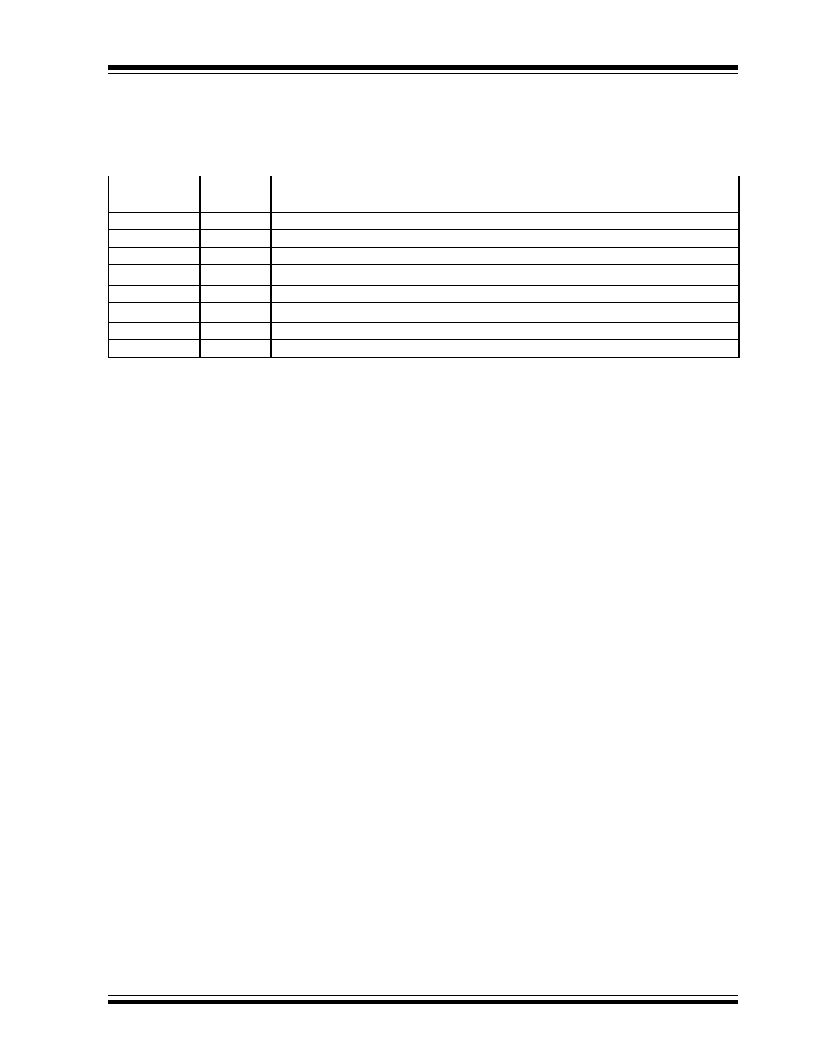
Device Selection Table
Package Type
General Description
The TC1682/TC1683/TC1684 are CMOS charge pump
converters that provide an inverted doubled output
from a single positive supply. An on-board oscillator
provides the clock and only three external capacitors
are required for full circuit implementation. Switching
frequencies are 12kHz for the TC1682, 35kHz for the
TC1683, and 125kHz for the TC1684. When the SHDN
pin is held at a logic high, the device goes into a very
low power mode of operation consuming less than 1
µ
A
(typ) of supply current.
Low output source impedance (typically 120
),
provides output current up to 10mA. The TC1682/
TC1683/TC1684 feature a 1.8V to 5.5V operating
voltage range and high efficiency, which make them an
ideal choice for a wide variety of applications requiring
a negative doubled voltage derived from a single
positive supply (for example: generation of -7.2V from
a +3.6V lithium cell or -10V generated from a +5V logic
supply).
The minimum external part count, small physical size
and shutdown mode feature make this family of
products useful for a wide variety of negative bias
power supply applications.
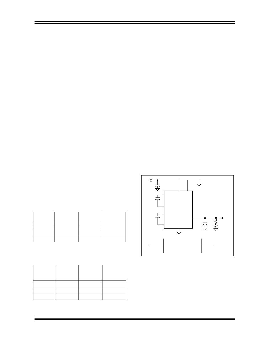
Functional Block Diagram
Part
Number
Package
Osc.
Freq.
(kHz)
Operating
Temp.
Range
TC1682EUA
8-Pin MSOP
12
-40∞C to +85∞C
TC1683EUA
8-Pin MSOP
35
-40∞C to +85∞C
TC1684EUA
8-Pin MSOP
125
-40∞C to +85∞C
1
2
3
4
8
7
6
5
TC1682
TC1683
TC1684
V
OUT
SHDN
V
IN
C2≠
GND
C1≠
C1+
C2+
8-Pin MSOP
C1+
C2+
V
IN
C1≠
C2
C2≠
C1
TC1682
TC1683
TC1684
V
OUT
+
+
+
≠ C
OUT
Input
GND
C1 must have a voltage rating
V
IN
C2 and C
OUT
must have a voltage rating
2V
IN
V
OUT
= -(2 x V
IN
)
SHDN
ON
OFF
Inverting Charge Pump Voltage Doublers with Active High Shutdown

TC1682/TC1683/TC1684
DS21537B-page 2
2002 Microchip Technology Inc.
1.0
ELECTRICAL
CHARACTERISTICS
Absolute Maximum Ratings*
Input Voltage (V
IN
to GND)....................... +6.0V, -0.3V
Output Voltage (V
OUT
to GND)............... -12.0V, +0.3V
Current at V
OUT
Pin.............................................20mA
Short-Circuit Duration V
OUT
to GND ..............Indefinite
Power Dissipation (T
A
70∞C)
8-Pin MSOP .............................................320mW
Operating Temperature Range............. -40∞C to +85∞C
Storage Temperature (Unbiased) .......-65∞C to +150∞C
*Stresses above those listed under "Absolute Maximum
Ratings" may cause permanent damage to the device. These
are stress ratings only and functional operation of the device
at these or any other conditions above those indicated in the
operation sections of the specifications is not implied.
Exposure to Absolute Maximum Rating conditions for
extended periods may affect device reliability.
TC1682/TC1683/TC1684 ELECTRICAL SPECIFICATIONS
Electrical Characteristics: T
A
= -40∞C to +85∞C, V
IN
= +5V, C1 = C2 = 3.3
µ
F (TC1682), C1 = C2 = 1
µ
F (TC1683),
C1 = C2 = 0.33
µ
F (TC1684), SHDN = GND, Typical values are at T
A
= +25∞C
Symbol
Parameter
Min
Typ
Max
Units
Device
Test Conditions
I
DD
Supply Current
--
--
--
95
225
700
160
480
1500
µ
A
TC1682
TC1683
TC1684
I
SHDN
Shutdown Supply Current
--
0.5
2
µ
A
All
SHDN = V
IN
= +5V
V
MIN
Minimum Supply Voltage
1.8
--
--
V
All
R
LOAD
= 1k
V
MAX
Maximum Supply Voltage
--
--
5.5
V
All
R
LOAD
= 1k
F
OSC
Oscillator Frequency
8.4
24.5
65
12
35
125
15.6
45.5
170
kHz
TC1682
TC1683
TC1684
V
IH
SHDN Input Logic High
1.4
--
--
V
All
V
IN
= V
MIN
to V
MAX
V
IL
SHDN Input Logic Low
--
--
0.4
V
All
V
IN
= V
MIN
to V
MAX
V
EFF
Voltage Conversion Efficiency
95
99
--
%
All
R
LOAD
=
R
OUT
Output Resistance
--
120
170
All
I
LOAD
= 0.5mA to 10mA (Note 1)
T
WK
Wake-up Time From Shutdown Mode
--
--
--
1800
600
200
--
--
--
µ
sec
TC1682
TC1683
TC1684
R
LOAD
= 2k
Note
1:
Capacitor contribution is approximately 20% of the output impedance (ESR = 1/ pump frequency x capacitance).
2002 Microchip Technology Inc.
DS21537B-page 3
TC1682/TC1683/TC1684
2.0
PIN DESCRIPTIONS
The descriptions of the pins are listed in Table 2-1.
TABLE 2-1:
PIN FUNCTION TABLE
Pin No.
(8-Pin MSOP)
Symbol
Description
1
C1≠
C1 commutation capacitor negative terminal.
2
C2+
C2 commutation capacitor positive terminal.
3
C2≠
C2 commutation capacitor negative terminal.
4
V
OUT
Doubling inverting charge pump output (-2 x V
IN
).
5
GND
Ground.
6
V
IN
Positive power supply input.
7
C1+
C1 commutation capacitor positive terminal.
8
SHDN
Shutdown input (active high).

TC1682/TC1683/TC1684
DS21537B-page 4
2002 Microchip Technology Inc.
3.0
DETAILED DESCRIPTION
The TC1682/TC1683/TC1684 inverting charge pump
converters perform a -2x multiplication of the voltage
applied to the V
IN
pin. Conversion is performed using
two synchronous switching matrices and three external
capacitors. When the shutdown input is held at a logic
high, the device goes into a very low power mode of
operation consuming less than 1
µ
A of supply current.
Figure 3-1 is a block diagram representation of the
TC1682/TC1683/TC1684 architecture. The first switch-
ing stage inverts the voltage present at V
IN
and the
second stage uses the `-V
IN
' output generated from the
first stage to produce the `-2X' output function from the
second stage switching matrix.
Each device contains an on-board oscillator that
synchronously controls the operation of the charge
pump switching matrices. The TC1682 synchronously
switches at 12kHz, the TC1683 synchronously
switches at 35kHz, and the TC1684 synchronously
switches at 125kHz. The different oscillator frequencies
for this device family allow the user to trade-off
capacitor size versus supply current. Faster oscillators
can use smaller external capacitors, but will consume
more supply current (see Section 1.0 Electrical
Characteristics).
When the shutdown input is in a high state, the
oscillator and both switch matrices are powered off
placing the TC1682/TC1683/TC1684 in the shutdown
mode. When the V
IN
supply input is powered from an
external battery, the shutdown mode minimizes power
consumption, which in turn will extend the life of the
battery.
FIGURE 3-1:
TC1682/TC1683/TC1684 ARCHITECTURE
SHDN
ENABLE
ENABLE
ENABLE
V
OUT
= -2V
IN
-V
IN
+
C
OUT
V
IN
Switch Matrix
(1st Stage)
Switch Matrix
(2nd Stage)
Oscillator
C1
+
C2
+
2002 Microchip Technology Inc.
DS21537B-page 5
TC1682/TC1683/TC1684
4.0
APPLICATIONS INFORMATION
4.1
Output Voltage Considerations
The TC1682/TC1683/TC1684 perform inverting
voltage conversions but do not provide any type of
regulation. The output voltage will droop in a linear
manner with respect to the output load current. The
value of the equivalent output resistance is
approximately 120
nominal at +25∞C and V
IN
= +5V.
In this particular case, the output is approximately -10V
at very light loads and will droop according to the
equation below:
V
DROOP
= I
OUT
x R
OUT
4.2
Capacitor Selection
In order to maintain the lowest output resistance and
output ripple voltage, it is recommended that low ESR
capacitors be used. Additionally, larger values of C1
and C2 will lower the output resistance and larger
values of C
OUT
will reduce output ripple.
Note:
For proper charge pump operation, C1
must have a voltage rating greater than or
equal to V
IN
, while C2 and C
OUT
must have
a voltage rating greater than or equal to
2V
IN
.
Table 4-1 shows various values of C1/C2 and the
corresponding output resistance values for V
IN
= 5V
@ +25∞C.
Table 4-2 shows the output voltage ripple for various
values of C
OUT
(again assuming V
IN
= 5V @ +25∞C).
The V
RIPPLE
values assume a 1mA output load current
and a 0.1
ESR
COUT
.
TABLE 4-1:
OUTPUT RESISTANCE
VS. C1/C2 (ESR = 0.1
)
TABLE 4-2:
OUTPUT VOLTAGE RIPPLE
VS. C
OUT2
(ESR = 0.1
)
I
OUT
= 1mA
4.3
Input Supply Bypassing
The V
IN
input should be capacitively bypassed to
reduce AC impedance and minimize noise effects due
to the switching internal to the device. It is
recommended that a large value capacitor (at least
equal to C1) be connected from V
IN
to GND for optimal
circuit performance.
4.4
Shutdown Input
The TC1682/TC1683/TC1684 is enabled when SHDN
is low, and disabled when SHDN is high. This input
cannot be allowed to float. (If SHDN is not required, see
the TC2682/TC2683/TC2684 data sheet.) The SHDN
input should be limited to 0.3V above V
IN
.
4.5
Inverting Voltage Doubler
The most common application for the TC1682/TC1683/
TC1684 devices is the inverting voltage doubler
(Figure 4-1). This application uses three external
capacitors: C1, C2 and C
OUT
.
Note:
A power supply bypass capacitor is
recommended.
The output is equal to -2V
IN
plus any voltage drops due
to loading. Refer to Table 4-1 and Table 4-2 for
capacitor selection guidelines.
FIGURE 4-1:
INVERTING VOLTAGE
DOUBLER TEST CIRCUIT
4.6
Layout Considerations
As with any switching power supply circuit, good layout
practice is recommended. Mount components as close
together as possible to minimize stray inductance and
capacitance. Also use a large ground plane to minimize
noise leakage into other circuitry.
C1, C2
(
µ
F)
TC1682
R
OUT
(
)
TC1683
R
OUT
(
)
TC1684
R
OUT
(
)
0.33
633
184
120
1
262
120
102
3.3
120
95
84
C
OUT
(
µ
F)
TC1682
V
RIPPLE
(mV)
TC1683
V
RIPPLE
(mV)
TC1684
V
RIPPLE
(mV)
0.33
192
60
27
1
63
21
16
3.3
17
8
7
C1
C2
V
IN
C
IN
V
OUT
R
L
V
IN
C
OUT
TC1682
TC1683
TC1684
C1≠
C2≠
2
1
7
6
8
4
5
3
C1+
C2+
GND
+
+
+
+
Device C
IN
C1
C2
C
OUT
TC1682 3.3
µF 3.3µF 3.3µF 3.3µF
TC1683 1
µF
1
µF 1µF 1µF
TC1684 0.33
µF 0.33µF 0.33µF 0.33µF
SHDN
V
OUT

TC1682/TC1683/TC1684
DS21537B-page 6
2002 Microchip Technology Inc.
5.0
PACKAGING INFORMATION
5.1
Package Marking Information
Package marking data not available at this time.
5.2
Taping Form
5.3
Package Dimensions
Component Taping Orientation for 8-Pin MSOP Devices
Package
Carrier Width (W)
Pitch (P)
Part Per Full Reel
Reel Size
8-Pin MSOP
12 mm
8 mm
2500
13 in
Carrier Tape, Number of Components Per Reel and Reel Size
User Direction of Feed
PIN 1
Standard Reel Component Orientation
for TR Suffix Device
P
8-Pin MSOP
.122 (3.10)
.114 (2.90)
.122 (3.10)
.114 (2.90)
.043 (1.10)
MAX.
.006 (0.15)
.002 (0.05)
.016 (0.40)
.010 (0.25)
.197 (5.00)
.189 (4.80)
.008 (0.20)
.005 (0.13)
.028 (0.70)
.016 (0.40)
6
∞ MAX.
.026 (0.65) TYP.
PIN 1
Dimensions: inches (mm)
2002 Microchip Technology Inc.
DS21537B-page 7
TC1682/TC1683/TC1684
Sales and Support
Data Sheets
Products supported by a preliminary Data Sheet may have an errata sheet describing minor operational differences and recom-
mended workarounds. To determine if an errata sheet exists for a particular device, please contact one of the following:
1.
Your local Microchip sales office
2.
The Microchip Corporate Literature Center U.S. FAX: (480) 792-7277
3.
The Microchip Worldwide Site (www.microchip.com)
Please specify which device, revision of silicon and Data Sheet (include Literature #) you are using.
New Customer Notification System
Register on our web site (www.microchip.com/cn) to receive the most current information on our products.

TC1682/TC1683/TC1684
DS21537B-page 8
2002 Microchip Technology Inc.
NOTES:

2002 Microchip Technology Inc.
DS21537B-page 9
TC1682/TC1683/TC1684
Information contained in this publication regarding device
applications and the like is intended through suggestion only
and may be superseded by updates. It is your responsibility to
ensure that your application meets with your specifications.
No representation or warranty is given and no liability is
assumed by Microchip Technology Incorporated with respect
to the accuracy or use of such information, or infringement of
patents or other intellectual property rights arising from such
use or otherwise. Use of Microchip's products as critical com-
ponents in life support systems is not authorized except with
express written approval by Microchip. No licenses are con-
veyed, implicitly or otherwise, under any intellectual property
rights.
Trademarks
The Microchip name and logo, the Microchip logo, FilterLab,
K
EE
L
OQ
, microID, MPLAB, PIC, PICmicro, PICMASTER,
PICSTART, PRO MATE, SEEVAL and The Embedded Control
Solutions Company are registered trademarks of Microchip Tech-
nology Incorporated in the U.S.A. and other countries.
dsPIC, ECONOMONITOR, FanSense, FlexROM, fuzzyLAB,
In-Circuit Serial Programming, ICSP, ICEPIC, microPort,
Migratable Memory, MPASM, MPLIB, MPLINK, MPSIM,
MXDEV, PICC, PICDEM, PICDEM.net, rfPIC, Select Mode
and Total Endurance are trademarks of Microchip Technology
Incorporated in the U.S.A.
Serialized Quick Turn Programming (SQTP) is a service mark
of Microchip Technology Incorporated in the U.S.A.
All other trademarks mentioned herein are property of their
respective companies.
© 2002, Microchip Technology Incorporated, Printed in the
U.S.A., All Rights Reserved.
Printed on recycled paper.
Microchip received QS-9000 quality system
certification for its worldwide headquarters,
design and wafer fabrication facilities in
Chandler and Tempe, Arizona in July 1999
and Mountain View, California in March 2002.
The Company's quality system processes and
procedures are QS-9000 compliant for its
PICmicro
Æ
8-bit MCUs, K
EE
L
OQ
Æ
code hopping
devices, Serial EEPROMs, microperipherals,
non-volatile memory and analog products. In
addition, Microchip's quality system for the
design and manufacture of development
systems is ISO 9001 certified.

DS21537B-page 10
2002 Microchip Technology Inc.
M
AMERICAS
Corporate Office
2355 West Chandler Blvd.
Chandler, AZ 85224-6199
Tel: 480-792-7200 Fax: 480-792-7277
Technical Support: 480-792-7627
Web Address: http://www.microchip.com
Rocky Mountain
2355 West Chandler Blvd.
Chandler, AZ 85224-6199
Tel: 480-792-7966 Fax: 480-792-7456
Atlanta
500 Sugar Mill Road, Suite 200B
Atlanta, GA 30350
Tel: 770-640-0034 Fax: 770-640-0307
Boston
2 Lan Drive, Suite 120
Westford, MA 01886
Tel: 978-692-3848 Fax: 978-692-3821
Chicago
333 Pierce Road, Suite 180
Itasca, IL 60143
Tel: 630-285-0071 Fax: 630-285-0075
Dallas
4570 Westgrove Drive, Suite 160
Addison, TX 75001
Tel: 972-818-7423 Fax: 972-818-2924
Detroit
Tri-Atria Office Building
32255 Northwestern Highway, Suite 190
Farmington Hills, MI 48334
Tel: 248-538-2250 Fax: 248-538-2260
Kokomo
2767 S. Albright Road
Kokomo, Indiana 46902
Tel: 765-864-8360 Fax: 765-864-8387
Los Angeles
18201 Von Karman, Suite 1090
Irvine, CA 92612
Tel: 949-263-1888 Fax: 949-263-1338
New York
150 Motor Parkway, Suite 202
Hauppauge, NY 11788
Tel: 631-273-5305 Fax: 631-273-5335
San Jose
Microchip Technology Inc.
2107 North First Street, Suite 590
San Jose, CA 95131
Tel: 408-436-7950 Fax: 408-436-7955
Toronto
6285 Northam Drive, Suite 108
Mississauga, Ontario L4V 1X5, Canada
Tel: 905-673-0699 Fax: 905-673-6509
ASIA/PACIFIC
Australia
Microchip Technology Australia Pty Ltd
Suite 22, 41 Rawson Street
Epping 2121, NSW
Australia
Tel: 61-2-9868-6733 Fax: 61-2-9868-6755
China - Beijing
Microchip Technology Consulting (Shanghai)
Co., Ltd., Beijing Liaison Office
Unit 915
Bei Hai Wan Tai Bldg.
No. 6 Chaoyangmen Beidajie
Beijing, 100027, No. China
Tel: 86-10-85282100 Fax: 86-10-85282104
China - Chengdu
Microchip Technology Consulting (Shanghai)
Co., Ltd., Chengdu Liaison Office
Rm. 2401, 24th Floor,
Ming Xing Financial Tower
No. 88 TIDU Street
Chengdu 610016, China
Tel: 86-28-6766200 Fax: 86-28-6766599
China - Fuzhou
Microchip Technology Consulting (Shanghai)
Co., Ltd., Fuzhou Liaison Office
Unit 28F, World Trade Plaza
No. 71 Wusi Road
Fuzhou 350001, China
Tel: 86-591-7503506 Fax: 86-591-7503521
China - Shanghai
Microchip Technology Consulting (Shanghai)
Co., Ltd.
Room 701, Bldg. B
Far East International Plaza
No. 317 Xian Xia Road
Shanghai, 200051
Tel: 86-21-6275-5700 Fax: 86-21-6275-5060
China - Shenzhen
Microchip Technology Consulting (Shanghai)
Co., Ltd., Shenzhen Liaison Office
Rm. 1315, 13/F, Shenzhen Kerry Centre,
Renminnan Lu
Shenzhen 518001, China
Tel: 86-755-2350361 Fax: 86-755-2366086
Hong Kong
Microchip Technology Hongkong Ltd.
Unit 901-6, Tower 2, Metroplaza
223 Hing Fong Road
Kwai Fong, N.T., Hong Kong
Tel: 852-2401-1200 Fax: 852-2401-3431
India
Microchip Technology Inc.
India Liaison Office
Divyasree Chambers
1 Floor, Wing A (A3/A4)
No. 11, O'Shaugnessey Road
Bangalore, 560 025, India
Tel: 91-80-2290061 Fax: 91-80-2290062
Japan
Microchip Technology Japan K.K.
Benex S-1 6F
3-18-20, Shinyokohama
Kohoku-Ku, Yokohama-shi
Kanagawa, 222-0033, Japan
Tel: 81-45-471- 6166 Fax: 81-45-471-6122
Korea
Microchip Technology Korea
168-1, Youngbo Bldg. 3 Floor
Samsung-Dong, Kangnam-Ku
Seoul, Korea 135-882
Tel: 82-2-554-7200 Fax: 82-2-558-5934
Singapore
Microchip Technology Singapore Pte Ltd.
200 Middle Road
#07-02 Prime Centre
Singapore, 188980
Tel: 65-6334-8870 Fax: 65-6334-8850
Taiwan
Microchip Technology Taiwan
11F-3, No. 207
Tung Hua North Road
Taipei, 105, Taiwan
Tel: 886-2-2717-7175 Fax: 886-2-2545-0139
EUROPE
Denmark
Microchip Technology Nordic ApS
Regus Business Centre
Lautrup hoj 1-3
Ballerup DK-2750 Denmark
Tel: 45 4420 9895 Fax: 45 4420 9910
France
Microchip Technology SARL
Parc d'Activite du Moulin de Massy
43 Rue du Saule Trapu
Batiment A - ler Etage
91300 Massy, France
Tel: 33-1-69-53-63-20 Fax: 33-1-69-30-90-79
Germany
Microchip Technology GmbH
Gustav-Heinemann Ring 125
D-81739 Munich, Germany
Tel: 49-89-627-144 0 Fax: 49-89-627-144-44
Italy
Microchip Technology SRL
Centro Direzionale Colleoni
Palazzo Taurus 1 V. Le Colleoni 1
20041 Agrate Brianza
Milan, Italy
Tel: 39-039-65791-1 Fax: 39-039-6899883
United Kingdom
Arizona Microchip Technology Ltd.
505 Eskdale Road
Winnersh Triangle
Wokingham
Berkshire, England RG41 5TU
Tel: 44 118 921 5869 Fax: 44-118 921-5820
03/01/02
' " $ '
W
ORLDWIDE
S
ALES
AND
S
ERVICE