800mA Fixed Low Dropout Positive Regulator
©
2002 Microchip Technology Inc.
DS21665B-page 1
TC2117
Features
· Fixed Output Voltages: 1.8V, 2.5V, 3.0V, 3.3V
· Very Low Dropout Voltage
· Rated 800mA Output Current
· High Output Voltage Accuracy
· Standard or Custom Output Voltages
· Over-Current and Over-Temperature Protection
· Space Saving SOT-223 Package
Applications
· 5V to 3.3V Linear Regulator
· Portable Computers
· Instrumentation
· Battery Operated Systems
· Linear Post-Regulator for SMPS
· Core Voltage Supply for FPGAs, PLDs, CPUs,
DSPs
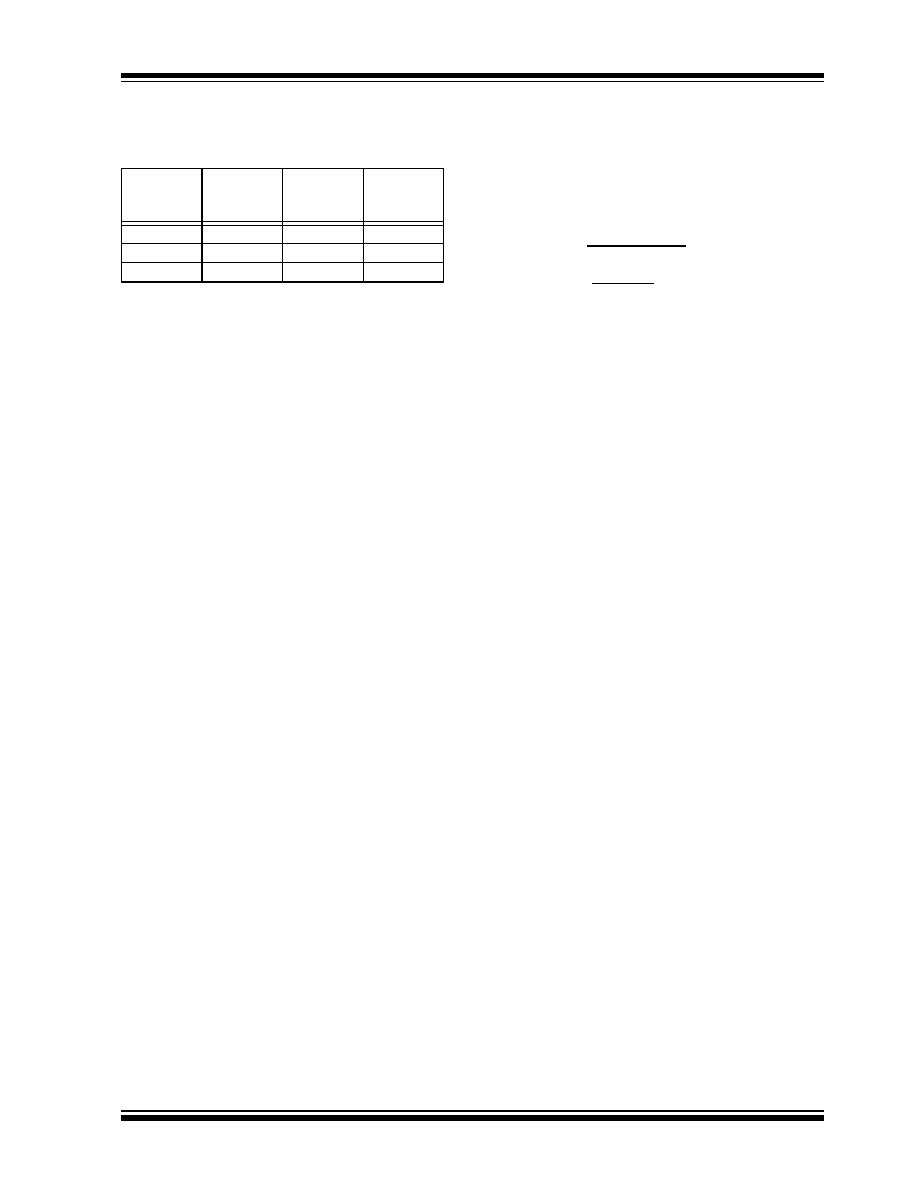
Device Selection Table
Note: xx indicates output voltages.
Available Output Voltages: 1.8, 2.5, 3.0, 3.3.
Other output voltages are available. Please contact Microchip
Technology Inc. for details.
Package Type
General Description
The TC2117 is a fixed, high accuracy (typically ±0.5%)
CMOS low dropout regulator. Designed specifically for
battery operated systems, the TC2117's CMOS con-
struction eliminates wasted ground current, signifi-
cantly extending battery life. Total supply current is
typically 80
µ
A at full load (20 to 60 times lower than in
bipolar regulators).
TC2117 key features include ultra low noise, very low
dropout voltage (typically 450mV at full load), and fast
response to step changes in load. The TC2117 incor-
porates both over-temperature and over-current pro-
tection. The TC2117 is stable with an output capacitor
of only 1
µ
F and has a maximum output current of
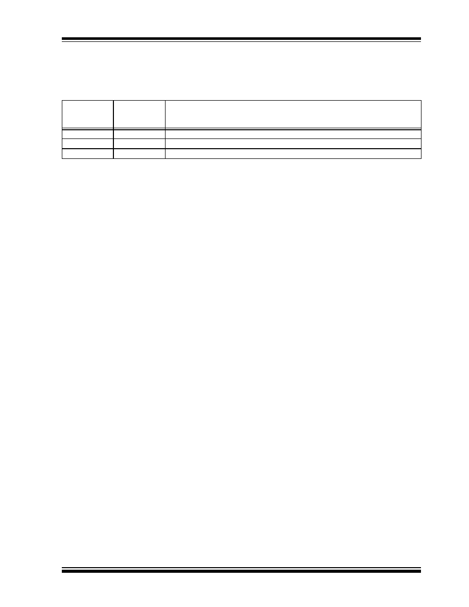
800mA. This device is available in 3-Pin SOT-223, and
3-Pin DDPAK packages.
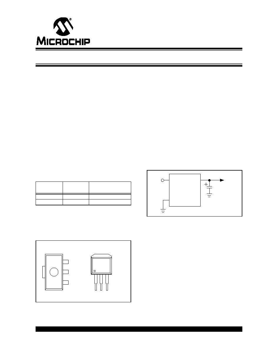
Typical Application
Part Number
Package
Junction
Temperature Range
TC2117-xxVDB 3-Pin SOT-223
-40°C to +125°C
TC2117-xxVEB
3-Pin DDPAK
-40°C to +125°C
V
IN
V
IN
V
OUT
GND
GND
V
OUT
Tab is V
OUT
Front View
Front View
1
1
2
3
3
2
Tab is V
OUT
TC2117
TC2117
3-Pin SOT-223
3-Pin DDPAK
TC2117
V
IN
V
OUT
C1
1
µF
GND
V
OUT
V
IN
800mA Fixed Low Dropout Positive Regulator
TC2117
DS21665B-page 2
©
2002 Microchip Technology Inc.
1.0
ELECTRICAL
CHARACTERISTICS
Absolute Maximum Ratings*
Input Voltage .........................................................6.5V
Output Voltage.................... (V
SS
0.3) to (V
IN
+ 0.3V)
Power Dissipation................Internally Limited (Note 7)
Maximum Voltage on Any Pin ......... V
IN
+0.3V to -0.3V
Operating Temperature ............... -40°C < T
J
< +125°C
Storage temperature .......................... -65°C to +150°C
*Stresses above those listed under "Absolute Maximum
Ratings" may cause permanent damage to the device. These
are stress ratings only and functional operation of the device
at these or any other conditions above those indicated in the
operation sections of the specifications is not implied.
Exposure to Absolute Maximum Rating conditions for
extended periods may affect device reliability.
TC2117 ELECTRICAL SPECIFICATIONS
Electrical Characteristics: V
IN
= V
R
+ 1.5V (Note 1), I
L
= 100
µ
A, C
L
= 3.3
µ
F, T
A
= 25°C, unless otherwise specified. Boldface type
specifications apply for junction temperatures of -40°C to +125°C.
Symbol
Parameter
Min
Typ
Max
Units
Test Conditions
V
IN
Input Operating Voltage
2.7
--
6.0
V
(Note 2)
I
OUT
MAX
Maximum Output Current
800
--
--
mA
V
OUT
Output Voltage
V
R
2.5%
V
R
2%
V
R
0.5%
V
R
0.5%
V
R
+ 2.5%
V
R
+ 3%
V
V
R
> 2.5V
V
R
= 1.8V
V
OUT
/
T
V
OUT
Temperature Coefficient
--
40
--
ppm/°C (Note 3)
V
OUT
/
V
IN
Line Regulation
--
0.007
0.35
%
(V
R
+ 1V) V
IN
6V
V
OUT
/V
OUT
Load Regulation
-0.01
0.002
0
%/mA
I
L
= 0.1mA to I
OUT
MAX
(Note 4)
V
IN
- V
OUT
Dropout Voltage
--
--
--
--
--
--
--
20
60
190
340
600
700
890
30
160
480
800
1300
1000
1400
mV
V
R
> 2.5V,
I
L
= 100
µ
A
I
L
= 100
µ
A
I
L
= 300
µ
A
I
L
= 500
µ
A
I
L
= 800
µ
A
V
R
= 1.8V,
I
L
= 500
µ
A
I
L
= 800
µ
A (Note 5)
I
DD
Supply Current
--
80
130
µ
A
I
L
= 0
PSRR
Power Supply Rejection Ratio
--
55
--
dB
F < 120Hz
I
OUT
SC
Output Short Circuit Current
--
1200
--
mA
V
OUT
= 0V
V
OUT
/
P
D
Thermal Regulation
--
0.04
--
V/W
(Note 6)
eN
Output Noise
--
300
--
nV/
Hz I
L
= 100mA, F = 10kHz
Note
1:
V
R
is the regulator output voltage setting.
2:
The minimum V
IN
has to justify the conditions: V
IN
V
R
+ V
DROPOUT
and V
IN
2.7V for I
L
= 0.1mA to I
OUT
MAX
.
3:
T
C
V
OUT
=
4:
Regulation is measured at a constant junction temperature using low duty cycle pulse testing. Load regulation is tested
over a load range from 0.1mA to the maximum specified output current. Changes in output voltage due to heating effects
are covered by the thermal regulation specification.
5:
Dropout voltage is defined as the input to output differential at which the output voltage drops 2% below its nominal value,
measured at a 1.5V differential.
6:
Thermal Regulation is defined as the change in output voltage at a time T after a change in power dissipation is applied,
excluding load or line regulation effects. Specifications are for a current pulse equal to I
L
MAX
at V
IN
= 6V for T = 10msec.
7:
The maximum allowable power dissipation is a function of ambient temperature, the maximum allowable junction
temperature, and the thermal resistance from junction-to-air (i.e., T
A
, T
J
,
JA
). Exceeding the maximum allowable power
dissipation causes the device to initiate thermal shutdown. Please see Thermal Considerations section of this data
sheet for more details.
(V
OUT
MAX
V
OUT
MIN
) x 10
6
V
OUT
x
T
©
2002 Microchip Technology Inc.
DS21665B-page 3
TC2117
2.0
PIN DESCRIPTIONS
The descriptions for the pins are listed in Table 2-1.
TABLE 2-1:
PIN FUNCTION TABLE
Pin No.
(3-Pin SOT-223)
(3-Pin DDPAK)
Symbol
Description
1
GND
Connect this pin to the circuit ground.
2
V
OUT
Regulated output voltage.
3
V
IN
Unregulated Input voltage.
TC2117
DS21665B-page 4
©
2002 Microchip Technology Inc.
3.0
DETAILED DESCRIPTION
The TC2117 is a precision, positive output LDO. Unlike
bipolar regulators, the TC2117 supply current does not
increase proportionally with load current. In addition,
V
OUT
remains stable and within regulation over the
entire 0mA to 800mA operating load range.
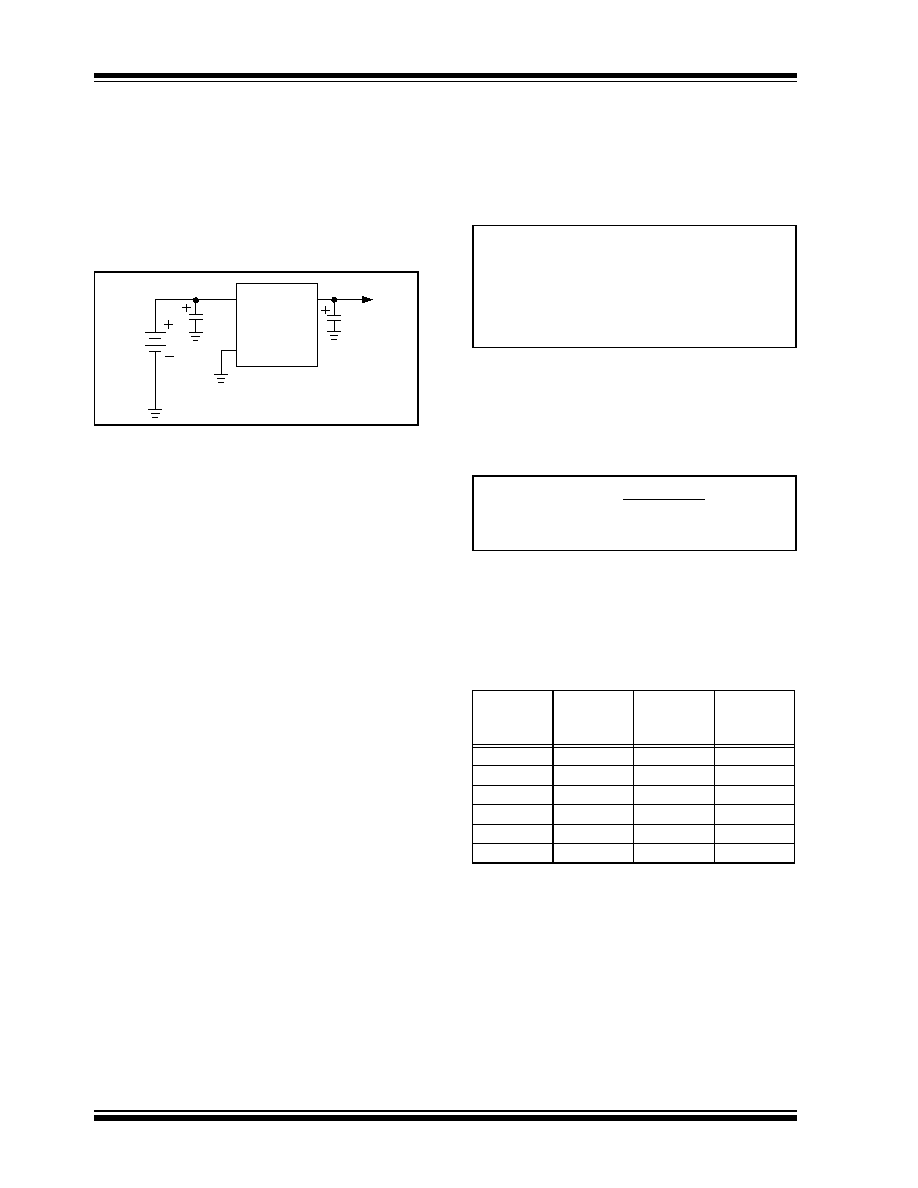
FIGURE 3-1:
TYPICAL APPLICATION
CIRCUIT
3.1
Output Capacitor
A 1
µ
F (min) capacitor from V
OUT
to ground is required.
The output capacitor should have an effective series
resistance of 0.2
to 10
. A 1
µ
F capacitor should be
connected from V
IN
to GND if there is more than 10
inches of wire between the regulator and the AC filter
capacitor, or if a battery is used as the power source.
Aluminum electrolytic or tantalum capacitor types can
be used. (Since many aluminum electrolytic capacitors
freeze at approximately -30°C, solid tantalums are rec-
ommended for applications operating below -25°C.)
When operating from sources other than batteries, sup-
ply noise rejection and transient response can be
improved by increasing the value of the input and output
capacitors and employing passive filtering techniques.
3.2
Thermal Considerations
3.2.1
THERMAL SHUTDOWN
Integrated thermal protection circuitry shuts the regula-
tor off when die temperature exceeds 160°C. The reg-
ulator remains off until the die temperature drops to
approximately 150°C.
3.2.2
POWER DISSIPATION
The amount of power the regulator dissipates is prima-
rily a function of input and output voltage, and output
current. The following equation is used to calculate
worst case actual power dissipation:
EQUATION 3-1:
The
maximum
allowable
power
dissipation
(Equation 3-2) is a function of the maximum ambient
temperature (T
A
MAX
), the maximum allowable die tem-
perature (125°C) and the thermal resistance from
junction-to-air (
JA
).
EQUATION 3-2:
Table 3-1 shows various values of
JA
for the TC2117
mounted on a 1/16 inch, 2-layer PCB with 1 oz. copper
foil.
TABLE 3-1:
THERMAL RESISTANCE
GUIDELINES FOR TC2117 IN
3-PIN SOT-223 PACKAGE
C1
1
µF
Battery
TC2117
V
IN
V
OUT
C2
1
µF
GND
V
OUT
Copper
Area
(Topside)*
Copper
Area
(Backside)
Board Area
Thermal
Resistance
2500 sq mm
2500 sq mm
2500 sq mm
45°C/W
1000 sq mm
2500 sq mm
2500 sq mm
45°C/W
225 sq mm
2500 sq mm
2500 sq mm
53°C/W
100 sq mm
2500 sq mm
2500 sq mm
59°C/W
1000 sq mm
1000 sq mm
1000 sq mm
52°C/W
1000 sq mm
0 sq mm
1000 sq mm
55°C/W
*Tab of device attached to topside copper.
P
D
(V
IN
MAX
V
OUT
MIN
)I
LOAD
MAX
Where:
P
D
= Worst case actual power dissipation
V
IN
MAX
= Maximum voltage on V
IN
V
OUT
MIN
= Maximum regulator output voltage
I
LOAD
MAX
= Maximum output (load) current
P
D
MAX
=
T
J
MAX
T
A
MAX
JA
Where all terms are previously defined.
©
2002 Microchip Technology Inc.
DS21665B-page 5
TC2117
TABLE 3-2:
THERMAL RESISTANCE
GUIDELINES FOR TC2117 IN
3-PIN DDPAK PACKAGE
Equation 3-1
can
be
used
in
conjunction
with
Equation 3-2 to ensure regulator thermal operation is
within limits. For example:
Find:
1. Actual power dissipation
2. Maximum allowable dissipation
Actual power dissipation:
Maximum allowable power dissipation:
In this example, the TC2117 dissipates a maximum of
only 786mW; below the allowable limit of 1.186mW. In
a similar manner, Equation 3-1 and Equation 3-2 can
be used to calculate maximum current and/or input
voltage limits.
Copper
Area
(Topside)*
Copper
Area
(Backside)
Board Area
Thermal
Resistance
(
JA
)
2500 sq mm
2500 sq mm
2500 sq mm
25°C/W
1000 sq mm
2500 sq mm
2500 sq mm
27°C/W
125 sq mm
2500 sq mm
2500 sq mm
35°C/W
*Tab of device attached to topside copper.
Given:
V
IN
MAX
=
5.0V ± 5%
V
OUT
MIN
=
3.3V ± 0.5%
I
LOADMAX
=
400mA
T
J
MAX
=
125°C
T
A
MAX
=
55°C
JA
=
59°C/W (SOT-223)
P
D
(V
IN
MAX
V
OUT
MIN
)I
LOAD
MAX
= [(5.0 x 1.05) (3.3 x .995)] 400 x 10
-3
= 786mW
P
D
MAX
=
(T
J
MAX
T
A
MAX
)
JA
=
(125 55)
59
=
1.186mW
TC2117
DS21665B-page 6
©
2002 Microchip Technology Inc.
4.0
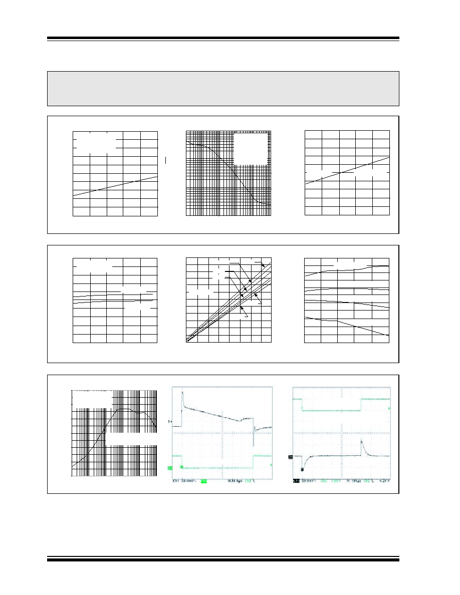
TYPICAL CHARACTERISTICS
Note:
The graphs and tables provided following this note are a statistical summary based on a limited number of
samples and are provided for informational purposes only. The performance characteristics listed herein
are not tested or guaranteed. In some graphs or tables, the data presented may be outside the specified
operating range (e.g., outside specified power supply range) and therefore outside the warranted range.
Output Noise vs. Frequency
FREQUENCY (kHz)
NOISE (
µ
V HZ)
10.0
1.0
0.01
0.01
1
10
100
1000
0.1
0.0
0.020
0.018
0.016
0.012
0.010
0.008
0.006
0.004
0.002
0.000
0.014
TEMPERATURE (
°C)
Line Regulation vs. Temperature
LINE REGULATION (%)
-40
°C
0
°C
0.0100
0.0090
0.0080
0.0070
0.0060
0.0050
0.0040
0.0030
0.0020
0.0010
0.0100
TEMPERATURE (°C)
Load Regulation vs. Temperature
LOAD REGULATION %/mA
1mA to 800mA
V
OUT
= 3V
V
IN
= 3.5V to 6.0V
V
OUT
= 2.5V
I
OUT
= 0.1mA
C
IN
= 1
µF
C = 1
µF
OUT
V = 6.0V
IN
V = 5V
OUT
I = 100mA
OUT
-40
°C 0°C
25
°C
70
°C
85
°C 125°C
25
°C
70
°C 85°C 125°C
0.600
0.550
0.500
0.450
0.400
0.350
0.300
0.250
0.200
0.150
0.100
0.050
0.000
0 100
200 300 400 500 600 700 800
I
LOAD
(mA)
Dropout Voltage vs. I
LOAD
DROPOUT VOLTAGE (V)
TEMPERATURE (°C)
I
DD
(
µ
A)
3.030
3.020
3.010
3.000
2.990
2.980
2.970
2.960
2.950
2.940
2.930
2.920
3.0V V
OUT
vs. Temperature
V
OUT
(V)
150
135
120
105
90
75
60
45
30
15
0
I
DD
vs. Temperature
85
°C
125
°C
-40
°C
0
°C
25
°C
70
°C
I
LOAD
= 0.1mA
I
LOAD
= 300mA
I
LOAD
= 500mA
I
LOAD
= 800mA
V
OUT
= 2.5V
V
OUT
= 5V
V
OUT
= 3V
V
IN
= V
OUT
+1V
I
OUT
= 0.1mA
-40
°C 0°C
25
°C
70
°C
85
°C 125°C
TEMPERATURE (°C)
-40
°C 0°C
25
°C
70
°C
85
°C 125°C
Power Supply Rejection Ratio
FREQUENCY (Hz)
PSRR (dB)
-70
-60
-50
-40
-30
-20
-10
10 100 1k
10k 100k 1M
V
OUT
I
OUT
= 300mA
V
IN
= 4.0V to 5.0V
C
OUT
= 10
µ
F Tantalum (0.25
ESR)
C
IN
= NA
Line Step Response
V
IN
= 4.0V
V
OUT
= 3.0V
C
IN
= 1
µ
F Ceramic
C
OUT
= 10
µ
F Tantalum (0.25
ESR)
I
OUT
= 6mA to 600mA
Load Step Response
V
INDC
= 4V
I
INAC
= 50mVp-p
V
OUTDC
= 3V
I
OUT
= 60mA
C
OUT
= 10
µ
F Tantalum
50mV/DIV
600mA/DIV
50mV/DIV
©
2002 Microchip Technology Inc.
DS21665B-page 7
TC2117
5.0
PACKAGING INFORMATION
5.1
Package Marking Information
Package marking information not available at this time.
5.2
Taping Information
Component Taping Orientation for 3-Pin SOT-223 Devices
Package
Carrier Width (W)
Pitch (P)
Part Per Full Reel
Reel Size
3-Pin SOT-223
12 mm
8 mm
4000
13 in
Carrier Tape, Number of Components Per Reel and Reel Size
User Direction of Feed
Device
Marking
PIN 1
Standard Reel Component Orientation
for TR Suffix Device
(Mark Right Side Up)
W
P
Component Taping Orientation for 3-Pin DDPAK Devices
Package
Carrier Width (W)
Pitch (P)
Part Per Full Reel
Reel Size
3-Pin DDPAK
24 mm
16 mm
750
13 in
Carrier Tape, Number of Components Per Reel and Reel Size
User Direction of Feed
Device
Marking
PIN 1
Standard Reel Component Orientation
for TR Suffix Device
(Mark Right Side Up)
W
P
TC2117
DS21665B-page 8
©
2002 Microchip Technology Inc.
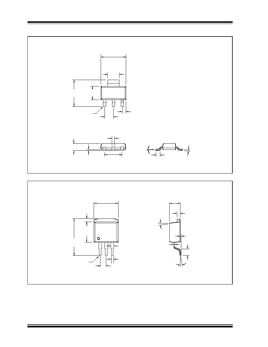
5.3
Packaging Dimensions
.264 (6.70)
.248 (6.30)
.122 (3.10)
.114 (2.90)
.287 (7.30)
.264 (6.70)
.146 (3.70)
.130 (3.30)
.091 (2.30) TYP.
.071
(1.80)
MAX.
.181 (4.60) TYP.
.036 (0.91) MIN.
.041 (1.04)
.033 (0.84)
PIN 1
.013 (0.33)
.009 (0.24)
.031 (0.80)
.024 (0.60)
.004 (0.10)
.001 (0.02)
10
°
MAX.
3-Pin SOT-223
Dimensions: inches (mm)
.100 (2.54) TYP.
3-Pin DDPAK
.037 (0.94)
.026 (0.66)
.370 (9.40)
.330 (8.38)
.067 (1.70)
.045 (1.14)
.605 (15.37)
.549 (13.95)
.410 (10.41)
.385 (9.78)
.183 (4.65)
.170 (4.32)
.055 (1.40)
.045 (1.14)
.010 (0.25)
.000 (0.00)
.110 (2.79)
.068 (1.72)
.026 (0.66)
.014 (0.36)
.051 (1.30)
.049 (1.24)
8
° MAX.
3
° - 7°
(5x)
PIN 1
Dimensions: inches (mm)

©
2002 Microchip Technology Inc.
DS21665B-page 9
TC2117
NOTES:

TC2117
DS21665B-page 10
©
2002 Microchip Technology Inc.
SALES AND SUPPORT
Data Sheets
Products supported by a preliminary Data Sheet may have an errata sheet describing minor operational differences and recom-
mended workarounds. To determine if an errata sheet exists for a particular device, please contact one of the following:
1.
Your local Microchip sales office
2.
The Microchip Corporate Literature Center U.S. FAX: (480) 792-7277
3.
The Microchip Worldwide Site (www.microchip.com)
Please specify which device, revision of silicon and Data Sheet (include Literature #) you are using.
New Customer Notification System
Register on our web site (www.microchip.com/cn) to receive the most current information on our products.
©
2002 Microchip Technology Inc.
DS21665B-page 11
TC2117
Information contained in this publication regarding device
applications and the like is intended through suggestion only
and may be superseded by updates. It is your responsibility to
ensure that your application meets with your specifications.
No representation or warranty is given and no liability is
assumed by Microchip Technology Incorporated with respect
to the accuracy or use of such information, or infringement of
patents or other intellectual property rights arising from such
use or otherwise. Use of Microchip's products as critical com-
ponents in life support systems is not authorized except with
express written approval by Microchip. No licenses are con-
veyed, implicitly or otherwise, under any intellectual property
rights.
Trademarks
The Microchip name and logo, the Microchip logo, FilterLab,
K
EE
L
OQ
, microID,
MPLAB, PIC, PICmicro, PICMASTER,
PICSTART, PRO MATE, SEEVAL and The Embedded Control
Solutions Company are registered trademarks of Microchip Tech-
nology Incorporated in the U.S.A. and other countries.
dsPIC, ECONOMONITOR, FanSense, FlexROM, fuzzyLAB,
In-Circuit Serial Programming, ICSP, ICEPIC, microPort,
Migratable Memory, MPASM, MPLIB, MPLINK, MPSIM,
MXDEV, PICC, PICDEM, PICDEM.net, rfPIC, Select Mode
and Total Endurance are trademarks of Microchip Technology
Incorporated in the U.S.A.
Serialized Quick Turn Programming (SQTP) is a service mark
of Microchip Technology Incorporated in the U.S.A.
All other trademarks mentioned herein are property of their
respective companies.
© 2002, Microchip Technology Incorporated, Printed in the
U.S.A., All Rights Reserved.
Printed on recycled paper.
Microchip received QS-9000 quality system
certification for its worldwide headquarters,
design and wafer fabrication facilities in
Chandler and Tempe, Arizona in July 1999
and Mountain View, California in March 2002.
The Company's quality system processes and
procedures are QS-9000 compliant for its
PICmicro
®
8-bit MCUs, K
EE
L
OQ
®
code hopping
devices, Serial EEPROMs, microperipherals,
non-volatile memory and analog products. In
addition, Microchip's quality system for the
design and manufacture of development
systems is ISO 9001 certified.

DS21665B-page 12
©
2002 Microchip Technology Inc.
AMERICAS
Corporate Office
2355 West Chandler Blvd.
Chandler, AZ 85224-6199
Tel: 480-792-7200 Fax: 480-792-7277
Technical Support: 480-792-7627
Web Address: http://www.microchip.com
Rocky Mountain
2355 West Chandler Blvd.
Chandler, AZ 85224-6199
Tel: 480-792-7966 Fax: 480-792-7456
Atlanta
500 Sugar Mill Road, Suite 200B
Atlanta, GA 30350
Tel: 770-640-0034 Fax: 770-640-0307
Boston
2 Lan Drive, Suite 120
Westford, MA 01886
Tel: 978-692-3848 Fax: 978-692-3821
Chicago
333 Pierce Road, Suite 180
Itasca, IL 60143
Tel: 630-285-0071 Fax: 630-285-0075
Dallas
4570 Westgrove Drive, Suite 160
Addison, TX 75001
Tel: 972-818-7423 Fax: 972-818-2924
Detroit
Tri-Atria Office Building
32255 Northwestern Highway, Suite 190
Farmington Hills, MI 48334
Tel: 248-538-2250 Fax: 248-538-2260
Kokomo
2767 S. Albright Road
Kokomo, Indiana 46902
Tel: 765-864-8360 Fax: 765-864-8387
Los Angeles
18201 Von Karman, Suite 1090
Irvine, CA 92612
Tel: 949-263-1888 Fax: 949-263-1338
New York
150 Motor Parkway, Suite 202
Hauppauge, NY 11788
Tel: 631-273-5305 Fax: 631-273-5335
San Jose
Microchip Technology Inc.
2107 North First Street, Suite 590
San Jose, CA 95131
Tel: 408-436-7950 Fax: 408-436-7955
Toronto
6285 Northam Drive, Suite 108
Mississauga, Ontario L4V 1X5, Canada
Tel: 905-673-0699 Fax: 905-673-6509
ASIA/PACIFIC
Australia
Microchip Technology Australia Pty Ltd
Suite 22, 41 Rawson Street
Epping 2121, NSW
Australia
Tel: 61-2-9868-6733 Fax: 61-2-9868-6755
China - Beijing
Microchip Technology Consulting (Shanghai)
Co., Ltd., Beijing Liaison Office
Unit 915
Bei Hai Wan Tai Bldg.
No. 6 Chaoyangmen Beidajie
Beijing, 100027, No. China
Tel: 86-10-85282100 Fax: 86-10-85282104
China - Chengdu
Microchip Technology Consulting (Shanghai)
Co., Ltd., Chengdu Liaison Office
Rm. 2401, 24th Floor,
Ming Xing Financial Tower
No. 88 TIDU Street
Chengdu 610016, China
Tel: 86-28-6766200 Fax: 86-28-6766599
China - Fuzhou
Microchip Technology Consulting (Shanghai)
Co., Ltd., Fuzhou Liaison Office
Unit 28F, World Trade Plaza
No. 71 Wusi Road
Fuzhou 350001, China
Tel: 86-591-7503506 Fax: 86-591-7503521
China - Shanghai
Microchip Technology Consulting (Shanghai)
Co., Ltd.
Room 701, Bldg. B
Far East International Plaza
No. 317 Xian Xia Road
Shanghai, 200051
Tel: 86-21-6275-5700 Fax: 86-21-6275-5060
China - Shenzhen
Microchip Technology Consulting (Shanghai)
Co., Ltd., Shenzhen Liaison Office
Rm. 1315, 13/F, Shenzhen Kerry Centre,
Renminnan Lu
Shenzhen 518001, China
Tel: 86-755-2350361 Fax: 86-755-2366086
Hong Kong
Microchip Technology Hongkong Ltd.
Unit 901-6, Tower 2, Metroplaza
223 Hing Fong Road
Kwai Fong, N.T., Hong Kong
Tel: 852-2401-1200 Fax: 852-2401-3431
India
Microchip Technology Inc.
India Liaison Office
Divyasree Chambers
1 Floor, Wing A (A3/A4)
No. 11, O'Shaugnessey Road
Bangalore, 560 025, India
Tel: 91-80-2290061 Fax: 91-80-2290062
Japan
Microchip Technology Japan K.K.
Benex S-1 6F
3-18-20, Shinyokohama
Kohoku-Ku, Yokohama-shi
Kanagawa, 222-0033, Japan
Tel: 81-45-471- 6166 Fax: 81-45-471-6122
Korea
Microchip Technology Korea
168-1, Youngbo Bldg. 3 Floor
Samsung-Dong, Kangnam-Ku
Seoul, Korea 135-882
Tel: 82-2-554-7200 Fax: 82-2-558-5934
Singapore
Microchip Technology Singapore Pte Ltd.
200 Middle Road
#07-02 Prime Centre
Singapore, 188980
Tel: 65-6334-8870 Fax: 65-6334-8850
Taiwan
Microchip Technology Taiwan
11F-3, No. 207
Tung Hua North Road
Taipei, 105, Taiwan
Tel: 886-2-2717-7175 Fax: 886-2-2545-0139
EUROPE
Denmark
Microchip Technology Nordic ApS
Regus Business Centre
Lautrup hoj 1-3
Ballerup DK-2750 Denmark
Tel: 45 4420 9895 Fax: 45 4420 9910
France
Microchip Technology SARL
Parc d'Activite du Moulin de Massy
43 Rue du Saule Trapu
Batiment A - ler Etage
91300 Massy, France
Tel: 33-1-69-53-63-20 Fax: 33-1-69-30-90-79
Germany
Microchip Technology GmbH
Gustav-Heinemann Ring 125
D-81739 Munich, Germany
Tel: 49-89-627-144 0 Fax: 49-89-627-144-44
Italy
Microchip Technology SRL
Centro Direzionale Colleoni
Palazzo Taurus 1 V. Le Colleoni 1
20041 Agrate Brianza
Milan, Italy
Tel: 39-039-65791-1 Fax: 39-039-6899883
United Kingdom
Arizona Microchip Technology Ltd.
505 Eskdale Road
Winnersh Triangle
Wokingham
Berkshire, England RG41 5TU
Tel: 44 118 921 5869 Fax: 44-118 921-5820
03/01/02
*DS21665B*
W
ORLDWIDE
S
ALES
AND
S
ERVICE