 | –≠–ª–µ–∫—Ç—Ä–æ–Ω–Ω—ã–π –∫–æ–º–ø–æ–Ω–µ–Ω—Ç: TC3682EUA | –°–∫–∞—á–∞—Ç—å:  PDF PDF  ZIP ZIP |

2002 Microchip Technology Inc.
DS21556B-page 1
M
TC3682/TC3683/TC3684
Features
∑ Small 8-Pin MSOP Package
∑ Operates from 1.8V to 5.5V
∑ 120 Ohms (typ) Output Resistance
∑ 99% Voltage Conversion Efficiency
∑ Only 3 External Capacitors Required
∑ Power-Saving Shutdown Mode
∑ Low Active Supply Current
- 95
µ
A (typ) for TC3682
- 225
µ
A (typ) for TC3683
- 700
µ
A (typ) for TC3684
∑ Fully Compatible with 1.8V Logic Systems
Applications
∑ LCD Panel Bias
∑ Cellular Phones PA Bias
∑ Pagers
∑ PDAs, Portable Data Loggers
∑ Battery-Powered Devices
Device Selection Table
Package Type
General Description
The TC3682/TC3683/TC3684 are CMOS charge pump
converters that provide an inverted doubled output
from a single positive supply. An on-board oscillator
provides the clock and only three external capacitors
are required for full circuit implementation. Switching
frequencies are 12kHz for the TC3682, 35kHz for the
TC3683, and 125kHz for the TC3684. When the SHDN
pin is held at a logic low, the device goes into a very low
power mode of operation consuming less than 1
µ
A
(typ) of supply current.
Low output source impedance (typically 120
), pro-
vides output current up to 10mA. The TC3682/TC3683/
TC3684 feature a 1.8V to 5.5V operating voltage range
and high efficiency, which make them an ideal choice
for a wide variety of applications requiring a negative
doubled voltage derived from a single positive supply
(for example: generation of -7.2V from a +3.6V lithium
cell or -10V generated from a +5V logic supply).
The minimum external part count, small physical size
and shutdown mode feature make this family of prod-
ucts useful for a wide variety of negative bias power
supply applications.
Functional Block Diagram
Part
Number
Package
Osc.
Freq.
(kHz)
Operating
Temp.
Range
TC3682EUA
8-Pin MSOP
12
-40∞C to +85∞C
TC3683EUA
8-Pin MSOP
35
-40∞C to +85∞C
TC3684EUA
8-Pin MSOP
125
-40∞C to +85∞C
1
2
3
4
8
7
6
5
TC3682
TC3683
TC3684
V
OUT
SHDN
V
IN
C2≠
GND
C1≠
C1+
C2+
8-Pin MSOP
C1+
C2+
V
IN
C1≠
C2
C2≠
C1
TC3682
TC3683
TC3684
V
OUT
+
+
+
≠ C
OUT
Input
GND
C1 must have a voltage rating
V
IN
C2 and C
OUT
must have a voltage rating
2V
IN
V
OUT
= -(2 x V
IN
)
SHDN
ON
OFF
Inverting Charge Pump Voltage Doublers with Active Low Shutdown

TC3682/TC3683/TC3684
DS21556B-page 2
2002 Microchip Technology Inc.
1.0
ELECTRICAL
CHARACTERISTICS
Absolute Maximum Ratings*
Input Voltage (V
IN
to GND)....................... +6.0V, -0.3V
Output Voltage (V
OUT
to GND) ............... -12.0V, +0.3V
Current at V
OUT
Pin.............................................20mA
Short-Circuit Duration V
OUT
to GND ..............Indefinite
Power Dissipation (T
A
70∞C)
8-Pin MSOP .............................................320mW
Operating Temperature Range............. -40∞C to +85∞C
Storage Temperature (Unbiased) .......-65∞C to +150∞C
*Stresses above those listed under "Absolute Maximum
Ratings" may cause permanent damage to the device. These
are stress ratings only and functional operation of the device
at these or any other conditions above those indicated in the
operation sections of the specifications is not implied.
Exposure to Absolute Maximum Rating conditions for
extended periods may affect device reliability.
TC3682/TC3683/TC3684 ELECTRICAL SPECIFICATIONS
Electrical Characteristics: T
A
= -40∞C to +85∞C, V
IN
= +5V, C1 = C2 = 3.3
µ
F (TC3682), C1 = C2 = 1
µ
F (TC3683),
C1 = C2 = 0.33
µ
F (TC3684), SHDN = GND, Typical values are at T
A
= +25∞C
Symbol
Parameter
Min
Typ
Max
Units
Device
Test Conditions
I
DD
Supply Current
--
--
--
95
225
700
160
480
1500
µ
A
TC3682
TC3683
TC3684
SHDN = V
IN
SHDN = V
IN
SHDN = V
IN
I
SHDN
Shutdown Supply Current
--
0.5
2
µ
A
All
SHDN = GND, V
IN
= +5V
V
MIN
Minimum Supply Voltage
1.8
--
--
V
All
R
LOAD
= 1k
V
MAX
Maximum Supply Voltage
--
--
5.5
V
All
R
LOAD
= 1k
F
OSC
Oscillator Frequency
8.4
24.5
65
12
35
125
15.6
45.5
170
kHz
TC3682
TC3683
TC3684
V
IH
SHDN Input Logic High
1.4
--
--
V
All
V
IN
= V
MIN
to V
MAX
V
IL
SHDN Input Logic Low
--
--
0.4
V
All
V
IN
= V
MIN
to V
MAX
V
EFF
Voltage Conversion Efficiency
95
99
--
%
All
R
LOAD
=
R
OUT
Output Resistance
--
120
170
All
I
LOAD
= 0.5mA to 10mA (Note 1)
T
WK
Wake-up Time From Shutdown Mode
--
--
--
1800
600
200
--
--
--
µ
sec
TC3682
TC3683
TC3684
R
LOAD
= 2k
Note
1:
Capacitor contribution is approximately 20% of the output impedance (ESR = 1/ pump frequency x capacitance).

2002 Microchip Technology Inc.
DS21556B-page 3
TC3682/TC3683/TC3684
2.0
PIN DESCRIPTIONS
The descriptions of the pins are listed in Table 2-1.
TABLE 2-1:
PIN FUNCTION TABLE
Pin No.
(8-Pin MSOP)
Symbol
Description
1
C1≠
C1 commutation capacitor negative terminal.
2
C2+
C2 commutation capacitor positive terminal.
3
C2≠
C2 commutation capacitor negative terminal.
4
V
OUT
Doubling inverting charge pump output (-2 x V
IN
).
5
GND
Ground.
6
V
IN
Positive power supply input.
7
C1+
C1 commutation capacitor positive terminal.
8
SHDN
Shutdown input (active low).

TC3682/TC3683/TC3684
DS21556B-page 4
2002 Microchip Technology Inc.
3.0
DETAILED DESCRIPTION
The TC3682/TC3683/TC3684 inverting charge pumps
perform a -2x multiplication of the voltage applied to
the V
IN
pin. Conversion is performed using two
synchronous switching matrices and three external
capacitors. When the shutdown input is held at a logic
low, the device goes into a very low power mode of
operation consuming less than 1
µ
A of supply current.
Figure 3-1 is a block diagram representation of the
TC3682/TC3683/TC3684 architecture. The first switch-
ing stage inverts the voltage present at V
IN
and the
second stage uses the `-V
IN
' output generated from the
first stage to produce the `-2X' output function from the
second stage switching matrix.
Each device contains an on-board oscillator that
synchronously controls the operation of the charge
pump switching matrices. The TC3682 synchronously
switches at 12kHz, the TC3683 synchronously
switches at 35kHz, and the TC3684 synchronously
switches at 125kHz. The different oscillator frequencies
for this device family allow the user to trade-off
capacitor size versus supply current. Faster oscillators
can use smaller external capacitors, but will consume
more supply current (see Section 1.0 Electrical
Characteristics).
When the shutdown input is in a low state, the oscillator
and both switch matrices are powered off placing the
TC3682/TC3683/TC3684 in the shutdown mode.
When the V
IN
supply input is powered from an external
battery, the shutdown mode minimizes power
consumption, which in turn will extend the life of the
battery.
FIGURE 3-1:
TC3682/TC3683/TC3684 ARCHITECTURE
SHDN
ENABLE
ENABLE
ENABLE
-2V
IN
-V
IN
+
C
OUT2
V
IN
Switch Matrix
(1st Stage)
Switch Matrix
(2nd Stage)
Oscillator
C1
+
C2
+
+
C
OUT1
2002 Microchip Technology Inc.
DS21556B-page 5
TC3682/TC3683/TC3684
4.0
APPLICATIONS INFORMATION
4.1
Output Voltage Considerations
The TC3682/TC3683/TC3684 perform inverting
voltage conversions but do not provide any type of
regulation. The output voltage will droop in a linear
manner with respect to the output load current. The
value of the equivalent output resistance of the `-V
IN
'
output is approximately 50
nominal at +25∞C and
V
IN
= +5V. The value of the `-2V
IN
' output is approxi-
mately 140
nominal at +25∞C and V
IN
= +5V. In this
particular case, `-V
IN
' is approximately -5V and `-2V
IN
'
is approximately -10V at very light loads and each
stage will droop according to the equation below:
V
DROOP
= I
OUT
x R
OUT
4.2
Capacitor Selection
In order to maintain the lowest output resistance and
output ripple voltage, it is recommended that low ESR
capacitors be used. Additionally, larger values of C1
and C2 will lower the output resistance and larger
values of C
OUT
will reduce output ripple.
Note:
For proper charge pump operation, C1
must have a voltage rating greater than or
equal to V
IN
, while C2 and C
OUT
must have
a voltage rating greater than or equal to
2V
IN
.
Table 4-1 shows various values of C1/C2 and the
corresponding output resistance values for V
IN
= 5V
@ +25∞C.
Table 4-2 shows the output voltage ripple for various
values of C
OUT
(again assuming V
IN
= 5V @ +25∞C).
The V
RIPPLE
values assume a 1mA output load current
and a 0.1
ESR
COUT
.
TABLE 4-1:
OUTPUT RESISTANCE
VS. C1/C2 (ESR = 0.1
)
TABLE 4-2:
OUTPUT VOLTAGE RIPPLE
VS. C
OUT
(ESR = 0.1
)
I
OUT
= 1mA
4.3
Input Supply Bypassing
The V
IN
input should be capacitively bypassed to
reduce AC impedance and minimize noise effects due
to the switching internal to the device. It is
recommended that a large value capacitor (at least
equal to C1) be connected from V
IN
to GND for optimal
circuit performance.
4.4
Shutdown Input
The TC3682/TC3683/TC3684 is enabled when SHDN
is high, and disabled when SHDN is low. This input
cannot be allowed to float. (If SHDN is not required, see
the TC2682/TC2683/TC2684 data sheet.) The SHDN
input should be limited to 0.3V above V
IN
.
4.5
Inverting Voltage Doubler
The most common application for the TC3682/TC3683/
TC3684 devices is the inverting voltage doubler
(Figure 4-1). This application uses three external
capacitors: C1, C2 and C
OUT
.
Note:
A power supply bypass capacitor is
recommended.
The output is equal to -2V
IN
plus any voltage drops due
to loading. Refer to Table 4-1 and Table 4-2 for
capacitor selection guidelines.
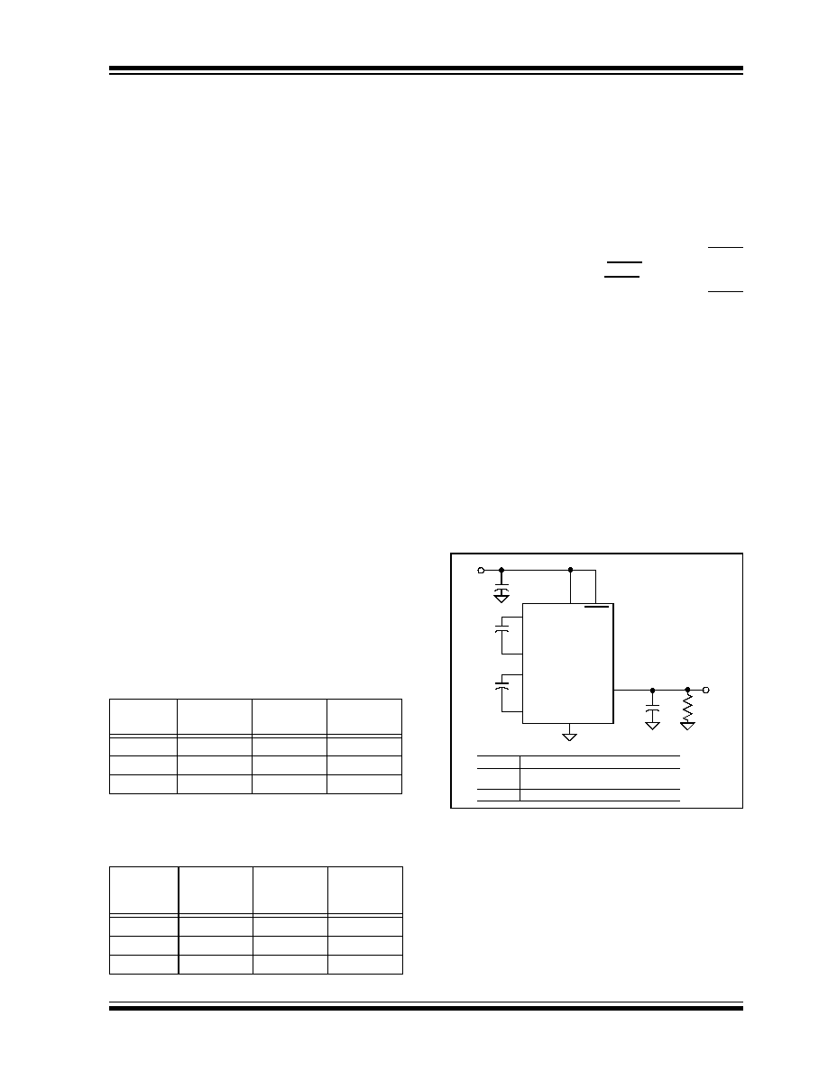
FIGURE 4-1:
INVERTING VOLTAGE
DOUBLER TEST CIRCUIT
4.6
Layout Considerations
As with any switching power supply circuit, good layout
practice is recommended. Mount components as close
together as possible to minimize stray inductance and
capacitance. Also use a large ground plane to minimize
noise leakage into other circuitry.
C1, C2
(
µ
F)
TC3682
R
OUT
(
)
TC3683
R
OUT
(
)
TC3684
R
OUT
(
)
0.33
633
184
120
1
262
120
102
3.3
120
95
84
C
OUT
(
µ
F)
TC3682
V
RIPPLE
(mV)
TC3683
V
RIPPLE
(mV)
TC3684
V
RIPPLE
(mV)
0.33
192
60
27
1
63
21
16
3.3
17
8
7
C1
C2
V
IN
C
IN
V
OUT
R
L
V
IN
C
OUT
TC3682
TC3683
TC3684
C1≠
C2≠
2
1
7
6
8
4
5
3
C1+
C2+
GND
+
+
+
+
Device C
IN
C1
C2
C
OUT
TC3682 3.3
µF 3.3µF 3.3µF 3.3µF
TC3683 1
µF
1
µF 1µF 1µF
TC3684 0.33
µF 0.33µF 0.33µF 0.33µF
SHDN
-2V
IN