 | –≠–ª–µ–∫—Ç—Ä–æ–Ω–Ω—ã–π –∫–æ–º–ø–æ–Ω–µ–Ω—Ç: TC427EPA | –°–∫–∞—á–∞—Ç—å:  PDF PDF  ZIP ZIP |

2002 Microchip Technology Inc.
DS21415B-page 1
M
TC426/TC427/TC428
Features
∑ High-Speed Switching (C
L
= 1000pF): 30nsec
∑ High Peak Output Current: 1.5A
∑ High Output Voltage Swing
- V
DD
-25mV
- GND +25mV
∑ Low Input Current (Logic "0" or "1"): 1
µ
A
∑ TTL/CMOS Input Compatible
∑ Available in Inverting and Noninverting
Configurations
∑ Wide Operating Supply Voltage
- 4.5V to 18V
∑ Current Consumption
- Inputs Low ≠ 0.4mA
- Inputs High ≠ 8mA
∑ Single Supply Operation
∑ Low Output Impedance: 6
∑ Pinout Equivalent of DS0026 and MMH0026
∑ Latch-Up Resistant: Withstands > 500mA
Reverse Current
∑ ESD Protected: 2kV
Applications
∑ Switch Mode Power Supplies
∑ Pulse Transformer Drive
∑ Clock Line Driver
∑ Coax Cable Driver
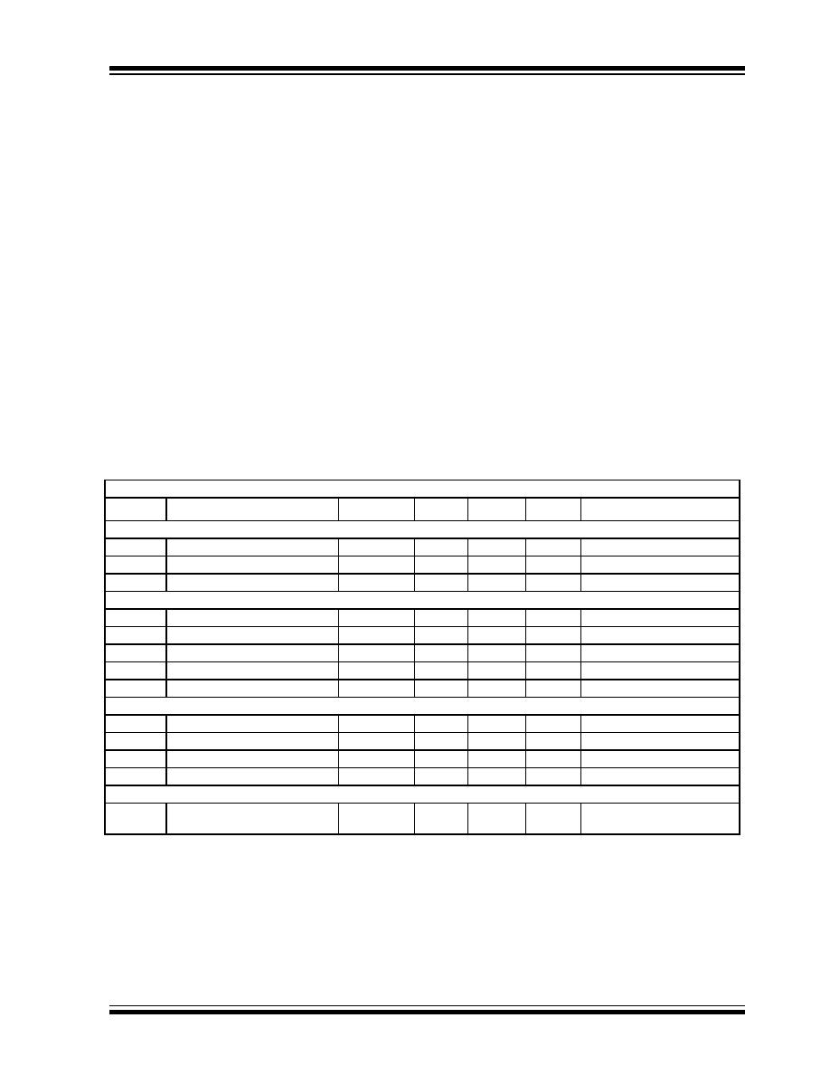
Device Selection Table
Package Type
General Description
The TC426/TC427/TC428 are dual CMOS high-speed
drivers. A TTL/CMOS input voltage level is translated
into a rail-to-rail output voltage level swing. The CMOS
output is within 25mV of ground or positive supply.
The low impedance, high-current driver outputs swing
a 1000pF load 18V in 30nsec. The unique current and
voltage drive qualities make the TC426/TC427/TC428
ideal power MOSFET drivers, line drivers, and DC-to-
DC converter building blocks.
Input logic signals may equal the power supply voltage.
Input current is a low 1
µ
A, making direct interface
to CMOS/bipolar switch-mode power supply control
ICs possible, as well as open-collector analog
comparators.
Quiescent power supply current is 8mA maximum. The
TC426 requires 1/5 the current of the pin-compatible
bipolar DS0026 device. This is important in DC-to-DC
converter applications with power efficiency constraints
and high-frequency switch-mode power supply
applications. Quiescent current is typically 6mA when
driving a 1000pF load 18V at 100kHz.
The inverting TC426 driver is pin-compatible with the
bipolar DS0026 and MMH0026 devices. The TC427 is
noninverting; the TC428 contains an inverting and non-
inverting driver.
Other pin compatible driver families are the TC1426/
TC1427/TC1428, TC4426/TC4427/TC4428 and
TC4426A/TC4427A/TC4428A.
Part
Number
Package
Configuration
Temp.
Range
TC426COA
TC426CPA
TC426EOA
TC426EPA
TC426IJA
TC426MJA
8-Pin SOIC
8-Pin PDIP
8-Pin SOIC
8-Pin PDIP
8-Pin CERDIP
8-Pin CERDIP
Inverting
Inverting
Inverting
Inverting
Inverting
Inverting
0∞C to +70∞C
0∞C to +70∞C
-40∞C to +85∞C
-40∞C to +85∞C
-25∞C to +85∞C
-55∞C to +125∞C
TC427COA
TC427CPA
TC427EOA
TC427EPA
TC427IJA
TC427MJA
8-Pin SOIC
8-Pin PDIP
8-Pin SOIC
8-Pin PDIP
8-Pin CERDIP
8-Pin CERDIP
Noninverting
Noninverting
Noninverting
Noninverting
Noninverting
Noninverting
0∞C to +70∞C
0∞C to +70∞C
-40∞C to +85∞C
-40∞C to +85∞C
-25∞C to +85∞C
-55∞C to +125∞C
TC428COA
TC428CPA
TC428EOA
TC428EPA
TC428IJA
TC428MJA
8-Pin SOIC
8-Pin PDIP
8-Pin SOIC
8-Pin PDIP
8-Pin CERDIP
8-Pin CERDIP
Complementary
Complementary
Complementary
Complementary
Complementary
Complementary
0∞C to +70∞C
0∞C to +70∞C
-40∞C to +85∞C
-40∞C to +85∞C
-25∞C to +85∞C
-55∞C to +125∞C
TC426
1
2
3
4
NC
5
6
7
8
OUT A
OUT B
NC
IN A
GND
IN B
NC = No internal connection
2, 4
7, 5
Inverting
TC427
1
2
3
4
NC
5
6
7
8
OUT A
OUT B
NC
IN A
GND
IN B
2, 4
7, 5
Noninverting
TC428
1
2
3
4
NC
5
6
7
8
OUT A
OUT B
NC
IN A
GND
IN B
2
7
4
5
V
DD
Complementary
V
DD
V
DD
8-Pin PDIP/SOIC/CERDIP
1.5A Dual High-Speed Power MOSFET Drivers

TC426/TC427/TC428
DS21415B-page 2
2002 Microchip Technology Inc.
Functional Block Diagram
Input
V+
2.5mA
500
µ
A
NOTE: TC428 has one inverting and one noninverting driver.
Ground any unused driver input.
Inverting
Output
Noninverting
Output
(TC426)
(TC427)
GND
TC426
TC427
TC428
2002 Microchip Technology Inc.
DS21415B-page 3
TC426/TC427/TC428
1.0
ELECTRICAL
CHARACTERISTICS
Absolute Maximum Ratings*
Supply Voltage..................................................... +20V
Input Voltage, Any Terminal
................................... V
DD
+ 0.3V to GND ≠ 0.3V
Power Dissipation (T
A
70∞C)
PDIP ........................................................ 730mW
CERDIP ................................................... 800mW
SOIC........................................................ 470mW
Derating Factor
PDIP ....................................................... 8mW/∞C
CERDIP ............................................... 6.4mW/∞C
SOIC....................................................... 4mW/∞C
Operating Temperature Range
C Version .........................................0∞C to +70∞C
I Version....................................... -25∞C to +85∞C
E Version ..................................... -40∞C to +85∞C
M Version................................... -55∞C to +125∞C
Storage Temperature Range ............. -65∞C to +150∞C
*Stresses above those listed under "Absolute Maximum
Ratings" may cause permanent damage to the device. These
are stress ratings only and functional operation of the device
at these or any other conditions above those indicated in the
operation sections of the specifications is not implied.
Exposure to Absolute Maximum Rating conditions for
extended periods may affect device reliability.
TC426/TC427/TC428 ELECTRICAL SPECIFICATIONS
Electrical Characteristics: T
A
= +25∞C with 4.5V
V
DD
18V, unless otherwise noted.
Symbol
Parameter
Min
Typ
Max
Units
Test Conditions
Input
V
IH
Logic 1, High Input Voltage
2.4
--
--
V
V
IL
Logic 0, Low Input Voltage
--
--
0.8
V
I
IN
Input Current
-1
--
1
µ
A
0V
V
IN
V
DD
Output
V
OH
High Output Voltage
V
DD
≠ 0.025
--
--
V
V
OL
Low Output Voltage
--
--
0.025
V
R
OH
High Output Resistance
--
10
15
I
OUT
= 10mA, V
DD
= 18V
R
OL
Low Output Resistance
--
6
10
I
OUT
= 10mA, V
DD
= 18V
I
PK
Peak Output Current
--
1.5
--
A
Switching Time (Note 1)
t
R
Rise Time
--
--
30
nsec
Figure 3-1, Figure 3-2
t
F
Fall Time
--
--
30
nsec
Figure 3-1, Figure 3-2
t
D1
Delay Time
--
--
50
nsec
Figure 3-1, Figure 3-2
t
D2
Delay Time
--
--
75
nsec
Figure 3-1, Figure 3-2
Power Supply
I
S
Power Supply Current
--
--
--
--
8
0.4
mA
V
IN
= 3V (Both Inputs)
V
IN
= 0V (Both Inputs)
Note
1:
Switching times ensured by design.

TC426/TC427/TC428
DS21415B-page 4
2002 Microchip Technology Inc.
TC426/TC427/TC428 ELECTRICAL SPECIFICATIONS (CONTINUED)
Electrical Characteristics: Over operating temperature range with 4.5V
V
DD
18V, unless otherwise noted.
Input
V
IH
Logic 1, High Input Voltage
2.4
--
--
V
V
IL
Logic 0, Low Input Voltage
--
--
0.8
V
I
IN
Input Current
-10
--
10
µ
A
0V
V
IN
V
DD
Output
V
OH
High Output Voltage
V
DD
≠ 0.025
--
--
V
V
OL
Low Output Voltage
--
--
0.025
V
R
OH
High Output Resistance
--
13
20
I
OUT
= 10mA, V
DD
= 18V
R
OL
Low Output Resistance
--
8
15
I
OUT
= 10mA, V
DD
= 18V
Switching Time (Note 1)
t
R
Rise Time
--
--
60
nsec
Figure 3-1, Figure 3-2
t
F
Fall Time
--
--
60
nsec
Figure 3-1, Figure 3-2
t
D1
Delay Time
--
--
75
nsec
Figure 3-1, Figure 3-2
t
D2
Delay Time
--
--
120
nsec
Figure 3-1, Figure 3-2
Power Supply
I
S
Power Supply Current
--
--
--
--
12
0.6
mA
V
IN
= 3V (Both Inputs)
V
IN
= 0V (Both Inputs)
Note
1:
Switching times ensured by design.
2002 Microchip Technology Inc.
DS21415B-page 5
TC426/TC427/TC428
2.0
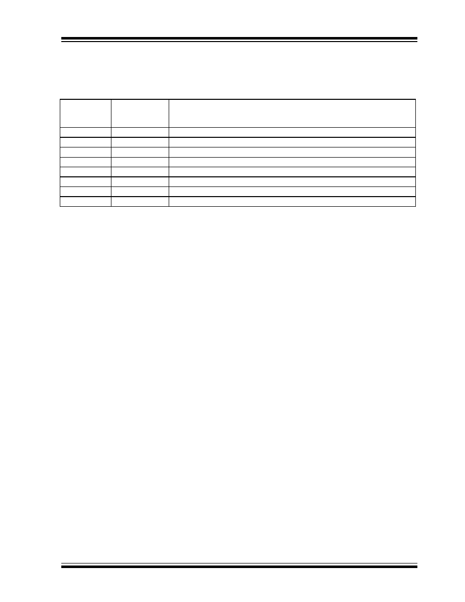
PIN DESCRIPTIONS
The descriptions of the pins are listed in Table 2-1.
TABLE 2-1:
PIN FUNCTION TABLE
Pin No.
(8-Pin PDIP,
SOIC, CERDIP)
Symbol
Description
1
NC
No Internal Connection.
2
IN A
Control Input A, TTL/CMOS compatible logic input.
3
GND
Ground.
4
IN B
Control Input B, TTL/CMOS compatible logic input.
5
OUT B
CMOS totem-pole output.
6
V
DD
Supply input, 4.5V to 18V.
7
OUT A
CMOS totem-pole output.
8
NC
No internal Connection.

TC426/TC427/TC428
DS21415B-page 6
2002 Microchip Technology Inc.
3.0
APPLICATIONS INFORMATION
3.1
Supply Bypassing
Charging and discharging large capacitive loads
quickly requires large currents. For example, charging
a 1000pF load to 18V in 25nsec requires an 0.72A
current from the device power supply.
To ensure low supply impedance over a wide frequency
range, a parallel capacitor combination is recom-
mended for supply bypassing. Low-inductance ceramic
disk capacitors with short lead lengths (< 0.5 in.) should
be used. A 1
µ
F film capacitor in parallel with one or two
0.1
µ
F ceramic disk capacitors normally provides
adequate bypassing.
3.2
Grounding
The TC426 and TC428 contain inverting drivers.
Ground potential drops developed in common ground
impedances from input to output will appear as
negative feedback and degrade switching speed
characteristics.
Individual ground returns for the input and output
circuits or a ground plane should be used.
3.3
Input Stage
The input voltage level changes the no-load or
quiescent supply current. The N-channel MOSFET
input stage transistor drives a 2.5mA current source
load. With a logic "1" input, the maximum quiescent
supply current is 8mA. Logic "0" input level signals
reduce quiescent current to 0.4mA maximum.
Minimum power dissipation occurs for logic "0" inputs
for the TC426/TC427/TC428. Unused driver inputs
must be connected to V
DD
or GND.
The drivers are designed with 100mV of hysteresis.
This provides clean transitions and minimizes output
stage current spiking when changing states. Input
voltage thresholds are approximately 1.5V, making the
device TTL compatible over the 4.5V to 18V supply
operating range. Input current is less than 1
µ
A over this
range.
The TC426/TC427/TC428 may be directly driven by
the TL494, SG1526/1527, SG1524, SE5560, and
similar switch-mode power supply integrated circuits.
3.4
Power Dissipation
The supply current vs frequency and supply current
vs capacitive load characteristic curves will aid in
determining power dissipation calculations.
The TC426/TC427/TC428 CMOS drivers have greatly
reduced quiescent DC power consumption. Maximum
quiescent current is 8mA compared to the DS0026
40mA specification. For a 15V supply, power
dissipation is typically 40mW.
Two other power dissipation components are:
∑ Output stage AC and DC load power.
∑ Transition state power.
Output stage power is:
Po = P
DC
+ PAC
= Vo (I
DC
) + f C
L
V
S
2
Where:
Vo = DC output voltage
I
DC
= DC output load current
f
= Switching frequency
Vs = Supply voltage
In power MOSFET drive applications the P
DC
term is
negligible. MOSFET power transistors are high imped-
ance, capacitive input devices. In applications where
resistive loads or relays are driven, the P
DC
component
will normally dominate.
The magnitude of P
AC
is readily estimated for several
cases:
A.
B.
1. f
= 200kHZ
1. f
= 200kHz
2. C
L
=1000pf
2. C
L
=1000pf
3. Vs
= 18V
3. Vs
= 15V
4. P
AC
= 65mW
4. P
AC
= 45mW
During output level state changes, a current surge will
flow through the series connected N and P channel
output MOSFETS as one device is turning "ON" while
the other is turning "OFF". The current spike flows only
during output transitions. The input levels should not be
maintained between the logic "0" and logic "1" levels.
Unused driver inputs must be tied to ground and
not be allowed to float. Average power dissipation will
be reduced by minimizing input rise times. As shown in
the characteristic curves, average supply current is
frequency dependent.

2002 Microchip Technology Inc.
DS21415B-page 7
TC426/TC427/TC428
FIGURE 3-1:
INVERTING DRIVER
SWITCHING TIME
TEST CIRCUIT
FIGURE 3-2:
NONINVERTING DRIVER
SWITCHING TIME
TEST CIRCUIT
FIGURE 3-3:
VOLTAGE DOUBLER
FIGURE 3-4:
VOLTAGE INVERTER
Output
Input
0.1
µF
V
DD
= 18V
+5V
Input
10%
90%
10%
90%
10%
90%
18V
Output
t
D1
t
F
t
R
t
D2
C
L
= 1000pF
1
µF
0V
0V
TC426
(1/2 TC428)
1
2
Input: 100kHz,
square wave,
t
RISE
= t
FALL
10nsec
Output
Input
90%
10%
10%
10%
90%
TC427
(1/2 TC428)
+5V
Input
18V
Output
0V
0V
90%
1
2
0.1
µF
1
µF
t
D1
t
F
t
R
t
D2
V
DD
= 18V
C
L
= 1000pF
Input: 100kHz,
square wave,
t
RISE
= t
FALL
10nsec
+15V
0.1
µF
4.7
µF
10
µF
47
µF
+
≠
+
≠
+
≠
1N4001
1N4001
V
OUT
f
IN
= 10kHz
2
6
3
7
29.
27.
25.
23.
0
10
20 30 40 50 60 70 80 90
I
OUT
(mA)
28.
26.
24.
22.
30.
100
V
OUT
(V)
1/2
TC426
+15V
0.1
µF 4.7µF
10
µF
47
µF
+
≠
+
≠
1N4001
1N4001
2
6
3
7
1/2
TC426
+
≠
-6
-8
-10
-12
0
10 20 30 40 50 60 70 80 90
-7
-9
-11
-13
-5
-14
100
I
OUT
(mA)
V
OUT
(V)
V
OUT
f
IN
= 10kHz

TC426/TC427/TC428
DS21415B-page 8
2002 Microchip Technology Inc.
4.0
TYPICAL CHARACTERISTICS
Note:
The graphs and tables provided following this note are a statistical summary based on a limited number of
samples and are provided for informational purposes only. The performance characteristics listed herein are
not tested or guaranteed. In some graphs or tables, the data presented may be outside the specified
operating range (e.g., outside specified power supply range) and therefore outside the warranted range.
30
20
10
0
-25
0
25
150
TIME (ns)
Rise and Fall Times vs.
Temperature
40
50
75
100
125
TEMPERATURE (
∞C)
35
25
15
80
70
60
50
30
0
DELAY TIME (ns)
Delay Times vs. Supply Voltage
40
90
SUPPLY VOLTAGE (V)
5
10
15
20
t
D2
60
50
40
30
10
0
5
10
15
20
TIME (ns)
SUPPLY VOLTAGE (V)
70
t
R
t
F
C
L
= 1000pF
T
A
= +25
∞C
Rise and Fall Times vs.
Supply Voltage
20
C
L
= 1000pF
T
A
= +25
∞C
C
L
= 1000pF
V
DD
= 18V
t
R
t
F
t
D1
100
1
10
1000
10K
TIME (ns)
CAPACITIVE LOAD (pF)
Rise and Fall Times vs.
Capacitive Load
10
1K
100
90
80
70
60
40
30
0
-25
50
100
150
DELAY TIME (ns)
TEMPERATURE (
∞C)
Delay Times vs. Temperature
50
100
25
75
125
70
60
50
40
20
0
10
SUPPLY CURRENT (mA)
Supply Current vs.
Capacitive Load
30
80
400kHz
200kHz
20kHz
100
1000
10K
CAPACITIVE LOAD (pF)
10
C
L
= 1000pF
V
DD
= 18V
t
D2
t
D1
T
A
= +25
∞C
V
DD
= 18V
T
A
= +25
∞C
V
DD
= 18V
t
R
t
F
0.96
0.72
0.48
0.24
0
10
OUTPUT VOLTAGE (V)
Low Output vs. Voltage
1.20
20 30 40 50 60 70 80 90 100
CURRENT SUNK (mA)
10V
15V
1.76
1.32
0.88
0.44
0
10
High Output vs. Voltage
2.20
20 30 40 50 60 70 80 90 100
CURRENT SOURCED (mA)
18V
V
DD
≠
V
OUT
(V)
13V
20
10
0
1
SUPPL
Y CURRENT (mA)
Supply Current vs. Frequency
30
10
100
1000
FREQUENCY (kHz)
10V
5V
T
A
= +25
∞C
V
DD
= 5V
V
DD
= 8V
V
DD
= 18V
C
L
= 1000pF
T
A
= +25
∞C
T
A
= +25
∞C

2002 Microchip Technology Inc.
DS21415B-page 9
TC426/TC427/TC428
TYPICAL CHARACTERISTICS (CONTINUED)
0
20
15
10
5
0
SUPPLY VOLTAGE (V)
50
100
150
200
250
300
SUPPLY CURRENT (
µA)
Supply Voltage vs.
Quiescent Supply Current
No Load
Both Inputs Logic "0"
T
A
= +25
∞C
1
2
3
4
5
6
20
15
10
5
0
SUPPLY VOLTAGE (V)
SUPPLY CURRENT (mA)
Supply Voltage vs.
Quiescent Supply Current
No Load
Both Inputs Logic "1"
T
A
= +25
∞C
200
0
400
600
800
1000
1200
1400
1600
0
10
20
30
40
50
60
70
80
90
100
110
120
AMBIENT TEMPERATURE (
∞C)
MAX. POWER (mW)
8-Pin DIP
8-
8-Pin CERDIP
8-Pin SOIC
Thermal Derating Curves
TC426/TC427/TC428
DS21415B-page 10
2002 Microchip Technology Inc.
5.0
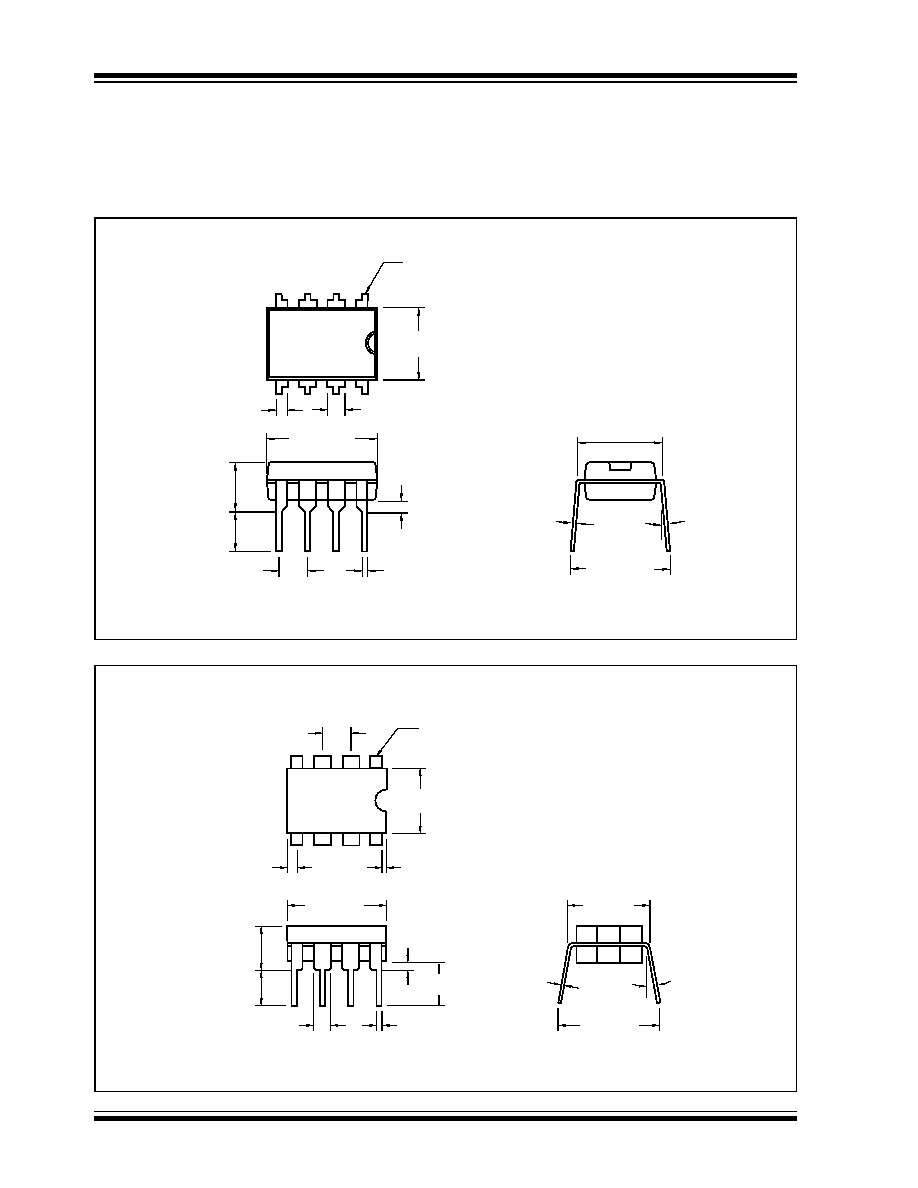
PACKAGING INFORMATION
5.1
Package Marking Information
Package marking data not available at this time.
5.2
Package Dimensions
3
∞ MIN.
PIN 1
.260 (6.60)
.240 (6.10)
.045 (1.14)
.030 (0.76)
.070 (1.78)
.040 (1.02)
.400 (10.16)
.348 (8.84)
.200 (5.08)
.140 (3.56)
.150 (3.81)
.115 (2.92)
.110 (2.79)
.090 (2.29)
.022 (0.56)
.015 (0.38)
.040 (1.02)
.020 (0.51)
.015 (0.38)
.008 (0.20)
.310 (7.87)
.290 (7.37)
.400 (10.16)
.310 (7.87)
8-Pin Plastic DIP
Dimensions: inches (mm)
.400 (10.16)
.370 (9.40)
.300 (7.62)
.230 (5.84)
.065 (1.65)
.045 (1.14)
.055 (1.40) MAX.
.020 (0.51) MIN.
PIN 1
.200 (5.08)
.160 (4.06)
.200 (5.08)
.125 (3.18)
.110 (2.79)
.090 (2.29)
.020 (0.51)
.016 (0.41)
.040 (1.02)
.020 (0.51)
.320 (8.13)
.290 (7.37)
.150 (3.81)
MIN.
3
∞ MIN.
8-Pin CERDIP (Narrow)
.015 (0.38)
.008 (0.20)
.400 (10.16)
.320 (8.13)
Dimensions: inches (mm)

2002 Microchip Technology Inc.
DS21415B-page 11
TC426/TC427/TC428
Package Dimensions (Continued)
.050 (1.27) TYP.
8
∞
MAX.
PIN 1
.244 (6.20)
.228 (5.79)
.157 (3.99)
.150 (3.81)
.197 (5.00)
.189 (4.80)
.020 (0.51)
.013 (0.33)
.010 (0.25)
.004 (0.10)
.069 (1.75)
.053 (1.35)
.010 (0.25)
.007 (0.18)
.050 (1.27)
.016 (0.40)
.
8-Pin SOIC
Dimensions: inches (mm)

TC426/TC427/TC428
DS21415B-page 12
2002 Microchip Technology Inc.
NOTES:

2002 Microchip Technology Inc.
DS21415B-page 13
TC426/TC427/TC428
Sales and Support
Data Sheets
Products supported by a preliminary Data Sheet may have an errata sheet describing minor operational differences and recom-
mended workarounds. To determine if an errata sheet exists for a particular device, please contact one of the following:
1.
Your local Microchip sales office
2.
The Microchip Corporate Literature Center U.S. FAX: (480) 792-7277
3.
The Microchip Worldwide Site (www.microchip.com)
Please specify which device, revision of silicon and Data Sheet (include Literature #) you are using.
New Customer Notification System
Register on our web site (www.microchip.com/cn) to receive the most current information on our products.

TC426/TC427/TC428
DS21415B-page 14
2002 Microchip Technology Inc.
NOTES:
2002 Microchip Technology Inc.
DS21415B-page 15
TC426/TC427/TC428
Information contained in this publication regarding device
applications and the like is intended through suggestion only
and may be superseded by updates. It is your responsibility to
ensure that your application meets with your specifications.
No representation or warranty is given and no liability is
assumed by Microchip Technology Incorporated with respect
to the accuracy or use of such information, or infringement of
patents or other intellectual property rights arising from such
use or otherwise. Use of Microchip's products as critical com-
ponents in life support systems is not authorized except with
express written approval by Microchip. No licenses are con-
veyed, implicitly or otherwise, under any intellectual property
rights.
Trademarks
The Microchip name and logo, the Microchip logo, FilterLab,
K
EE
L
OQ
, microID, MPLAB, PIC, PICmicro, PICMASTER,
PICSTART, PRO MATE, SEEVAL and The Embedded Control
Solutions Company are registered trademarks of Microchip Tech-
nology Incorporated in the U.S.A. and other countries.
dsPIC, ECONOMONITOR, FanSense, FlexROM, fuzzyLAB,
In-Circuit Serial Programming, ICSP, ICEPIC, microPort,
Migratable Memory, MPASM, MPLIB, MPLINK, MPSIM,
MXDEV, PICC, PICDEM, PICDEM.net, rfPIC, Select Mode
and Total Endurance are trademarks of Microchip Technology
Incorporated in the U.S.A.
Serialized Quick Turn Programming (SQTP) is a service mark
of Microchip Technology Incorporated in the U.S.A.
All other trademarks mentioned herein are property of their
respective companies.
© 2002, Microchip Technology Incorporated, Printed in the
U.S.A., All Rights Reserved.
Printed on recycled paper.
Microchip received QS-9000 quality system
certification for its worldwide headquarters,
design and wafer fabrication facilities in
Chandler and Tempe, Arizona in July 1999
and Mountain View, California in March 2002.
The Company's quality system processes and
procedures are QS-9000 compliant for its
PICmicro
Æ
8-bit MCUs, K
EE
L
OQ
Æ
code hopping
devices, Serial EEPROMs, microperipherals,
non-volatile memory and analog products. In
addition, Microchip's quality system for the
design and manufacture of development
systems is ISO 9001 certified.

DS21415B-page 16
2002 Microchip Technology Inc.
M
AMERICAS
Corporate Office
2355 West Chandler Blvd.
Chandler, AZ 85224-6199
Tel: 480-792-7200 Fax: 480-792-7277
Technical Support: 480-792-7627
Web Address: http://www.microchip.com
Rocky Mountain
2355 West Chandler Blvd.
Chandler, AZ 85224-6199
Tel: 480-792-7966 Fax: 480-792-7456
Atlanta
500 Sugar Mill Road, Suite 200B
Atlanta, GA 30350
Tel: 770-640-0034 Fax: 770-640-0307
Boston
2 Lan Drive, Suite 120
Westford, MA 01886
Tel: 978-692-3848 Fax: 978-692-3821
Chicago
333 Pierce Road, Suite 180
Itasca, IL 60143
Tel: 630-285-0071 Fax: 630-285-0075
Dallas
4570 Westgrove Drive, Suite 160
Addison, TX 75001
Tel: 972-818-7423 Fax: 972-818-2924
Detroit
Tri-Atria Office Building
32255 Northwestern Highway, Suite 190
Farmington Hills, MI 48334
Tel: 248-538-2250 Fax: 248-538-2260
Kokomo
2767 S. Albright Road
Kokomo, Indiana 46902
Tel: 765-864-8360 Fax: 765-864-8387
Los Angeles
18201 Von Karman, Suite 1090
Irvine, CA 92612
Tel: 949-263-1888 Fax: 949-263-1338
New York
150 Motor Parkway, Suite 202
Hauppauge, NY 11788
Tel: 631-273-5305 Fax: 631-273-5335
San Jose
Microchip Technology Inc.
2107 North First Street, Suite 590
San Jose, CA 95131
Tel: 408-436-7950 Fax: 408-436-7955
Toronto
6285 Northam Drive, Suite 108
Mississauga, Ontario L4V 1X5, Canada
Tel: 905-673-0699 Fax: 905-673-6509
ASIA/PACIFIC
Australia
Microchip Technology Australia Pty Ltd
Suite 22, 41 Rawson Street
Epping 2121, NSW
Australia
Tel: 61-2-9868-6733 Fax: 61-2-9868-6755
China - Beijing
Microchip Technology Consulting (Shanghai)
Co., Ltd., Beijing Liaison Office
Unit 915
Bei Hai Wan Tai Bldg.
No. 6 Chaoyangmen Beidajie
Beijing, 100027, No. China
Tel: 86-10-85282100 Fax: 86-10-85282104
China - Chengdu
Microchip Technology Consulting (Shanghai)
Co., Ltd., Chengdu Liaison Office
Rm. 2401, 24th Floor,
Ming Xing Financial Tower
No. 88 TIDU Street
Chengdu 610016, China
Tel: 86-28-6766200 Fax: 86-28-6766599
China - Fuzhou
Microchip Technology Consulting (Shanghai)
Co., Ltd., Fuzhou Liaison Office
Unit 28F, World Trade Plaza
No. 71 Wusi Road
Fuzhou 350001, China
Tel: 86-591-7503506 Fax: 86-591-7503521
China - Shanghai
Microchip Technology Consulting (Shanghai)
Co., Ltd.
Room 701, Bldg. B
Far East International Plaza
No. 317 Xian Xia Road
Shanghai, 200051
Tel: 86-21-6275-5700 Fax: 86-21-6275-5060
China - Shenzhen
Microchip Technology Consulting (Shanghai)
Co., Ltd., Shenzhen Liaison Office
Rm. 1315, 13/F, Shenzhen Kerry Centre,
Renminnan Lu
Shenzhen 518001, China
Tel: 86-755-2350361 Fax: 86-755-2366086
Hong Kong
Microchip Technology Hongkong Ltd.
Unit 901-6, Tower 2, Metroplaza
223 Hing Fong Road
Kwai Fong, N.T., Hong Kong
Tel: 852-2401-1200 Fax: 852-2401-3431
India
Microchip Technology Inc.
India Liaison Office
Divyasree Chambers
1 Floor, Wing A (A3/A4)
No. 11, O'Shaugnessey Road
Bangalore, 560 025, India
Tel: 91-80-2290061 Fax: 91-80-2290062
Japan
Microchip Technology Japan K.K.
Benex S-1 6F
3-18-20, Shinyokohama
Kohoku-Ku, Yokohama-shi
Kanagawa, 222-0033, Japan
Tel: 81-45-471- 6166 Fax: 81-45-471-6122
Korea
Microchip Technology Korea
168-1, Youngbo Bldg. 3 Floor
Samsung-Dong, Kangnam-Ku
Seoul, Korea 135-882
Tel: 82-2-554-7200 Fax: 82-2-558-5934
Singapore
Microchip Technology Singapore Pte Ltd.
200 Middle Road
#07-02 Prime Centre
Singapore, 188980
Tel: 65-6334-8870 Fax: 65-6334-8850
Taiwan
Microchip Technology Taiwan
11F-3, No. 207
Tung Hua North Road
Taipei, 105, Taiwan
Tel: 886-2-2717-7175 Fax: 886-2-2545-0139
EUROPE
Denmark
Microchip Technology Nordic ApS
Regus Business Centre
Lautrup hoj 1-3
Ballerup DK-2750 Denmark
Tel: 45 4420 9895 Fax: 45 4420 9910
France
Microchip Technology SARL
Parc d'Activite du Moulin de Massy
43 Rue du Saule Trapu
Batiment A - ler Etage
91300 Massy, France
Tel: 33-1-69-53-63-20 Fax: 33-1-69-30-90-79
Germany
Microchip Technology GmbH
Gustav-Heinemann Ring 125
D-81739 Munich, Germany
Tel: 49-89-627-144 0 Fax: 49-89-627-144-44
Italy
Microchip Technology SRL
Centro Direzionale Colleoni
Palazzo Taurus 1 V. Le Colleoni 1
20041 Agrate Brianza
Milan, Italy
Tel: 39-039-65791-1 Fax: 39-039-6899883
United Kingdom
Arizona Microchip Technology Ltd.
505 Eskdale Road
Winnersh Triangle
Wokingham
Berkshire, England RG41 5TU
Tel: 44 118 921 5869 Fax: 44-118 921-5820
03/01/02
' !" '
W
ORLDWIDE
S
ALES
AND
S
ERVICE