 | –≠–ª–µ–∫—Ç—Ä–æ–Ω–Ω—ã–π –∫–æ–º–ø–æ–Ω–µ–Ω—Ç: TC4404MJA | –°–∫–∞—á–∞—Ç—å:  PDF PDF  ZIP ZIP |

2002 Microchip Technology Inc.
DS21418B-page 1
M
TC4404/TC4405
Features
∑ Independently Programmable Rise and Fall
Times
∑ Low Output Impedance ≠ 7
Typ.
∑ High Speed t
R
, t
F
≠
<30nsec with 1000pF Load
∑ Short Delay Times ≠ <30nsec
∑ Wide Operating Range
- 4.5V to 18V
∑ Latch-Up Protected: Will Withstand > 500mA
Reverse Current (Either Polarity)
∑ Input Withstands Negative Swings Up to -5V
Applications
∑ Motor Controls
∑ Driving Bipolar Transistors
∑ Driver for Non-overlapping Totem Poles
∑ Reach-Up/Reach-Down Driver
Device Selection Table
General Description
The TC4404/TC4405 are CMOS buffer-drivers
constructed with complementary MOS outputs, where
the drains of the totem-pole output have been left
separated so that individual connections can be made
to the pull-up and pull-down sections of the output. This
allows the insertion of drain-current-limiting resistors in
the pull-up and/or pull-down sections, allowing the user
to define the rates of rise and fall for a capacitive load;
or a reduced output swing, if driving a resistive load, or
to limit base current, when driving a bipolar transistor.
Minimum rise and fall times, with no resistors, will be
less than 30nsec for a 1000pF load.
For driving MOSFETs in motor-control applications,
where slow-ON/fast-OFF operation is desired, these
devices are superior to the previously used technique
of adding a diode-resistor combination between the
driver output and the MOSFET, because they allow
accurate control of turn-ON, while maintaining fast turn-
OFF and maximum noise immunity for an OFF device.
When used to drive bipolar transistors, these drivers
maintain the high speeds common to other Microchip
drivers. They allow insertion of a base current-limiting
resistor, while providing a separate half-output for fast
turn-OFF. By proper positioning of the resistor, either
npn or pnp transistors can be driven.
For driving many loads in low-power regimes, these
drivers, because they eliminate shoot-through currents
in the output stage, require significantly less power at
higher frequencies, and can be helpful in meeting
low-power budgets.
Package Type
Part Number
Package
Temp. Range
TC4404COA
8-Pin SOIC
0∞C to +70∞C
TC4404CPA
8-Pin PDIP
0∞C to +70∞C
TC4404EOA
8-Pin SOIC
-40∞C to +85∞C
TC4404EPA
8-Pin PDIP
-40∞C to +85∞C
TC4404MJA
8-Pin CERDIP
-55∞C to +125∞C
TC4405COA
8-Pin SOIC
0∞C to +70∞C
TC4405CPA
8-Pin PDIP
0∞C to +70∞C
TC4405EOA
8-Pin SOIC
-40∞C to +85∞C
TC4405EPA
8-Pin PDIP
-40∞C to +85∞C
TC4405MJA
8-Pin CERDIP
-55∞C to +125∞C
1
8
2
7
3
6
4
5
TC4405
B BOTTOM
GND
IN B
IN A
V
DD
B TOP
A BOTTOM
A TOP
1
8
2
7
3
6
4
5
TC4405
B BOTTOM
GND
IN B
IN A
V
DD
B TOP
A BOTTOM
A TOP
1
8
2
7
3
6
4
5
TC4404
B BOTTOM
GND
IN B
IN A
V
DD
B TOP
A BOTTOM
A TOP
1
8
2
7
3
6
4
5
TC4404
B BOTTOM
GND
IN B
IN A
V
DD
B TOP
A BOTTOM
A TOP
8-Pin PDIP/SOIC/CERDIP
1.5A Dual Open-Drain MOSFET Drivers
TC4404/TC4405
DS21418B-page 2
2002 Microchip Technology Inc.
Because neither drain in an output is dependent on the
other, these devices can also be used as open-drain
buffer/drivers where both drains are available in one
device, thus minimizing chip count. Unused open
drains should be returned to the supply rail that their
device sources are connected to (pull-downs to
ground, pull-ups to V
DD
), to prevent static damage. In
addition, in situations where timing resistors or other
means of limiting crossover currents are used, like
drains may be paralleled for greater current carrying
capacity.
These devices are built to operate in the most demand-
ing electrical environments. They will not latch up under
any conditions within their power and voltage ratings;
they are not subject to damage when up to 5V of noise
spiking of either polarity occurs on their ground pin; and
they can accept, without damage or logic upset, up to
1/2 amp of reverse current (of either polarity) being
forced back into their outputs. All terminals are fully
protected against up to 2kV of electrostatic discharge.
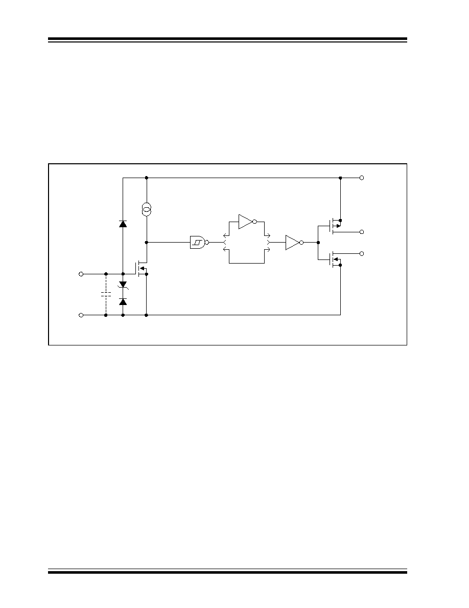
Functional Block Diagram
Input
GND
Effective
Input
C
12 pF
300 mV
V
DD
Pull Up
Pull Down
2 (3)
A (B)
8 (6)
7 (5)
4
1
TC4404
Inverting
TC4405
Noninverting
4.7V

2002 Microchip Technology Inc.
DS21418B-page 3
TC4404/TC4405
1.0
ELECTRICAL
CHARACTERISTICS
Absolute Maximum Ratings*
Supply Voltage..................................................... +22V
Power Dissipation (T
A
70∞C)
PDIP ........................................................ 730mW
CERDIP ................................................... 800mW
SOIC........................................................ 470mW
Package Thermal Resistance
PDIP R
J-A
............................................. 125∞C/W
PDIP R
J-C
............................................... 45∞C/W
CERDIP R
J-A
.........................................150
∞
C/W
CERDIP R
J-C
......................................... 55∞C/W
SOIC R
J-A
............................................ 155∞C/W
SOIC R
J-C
.............................................. 45∞C/W
Operating Temperature Range
C Version .........................................0∞C to +70∞C
E Version ..................................... -40∞C to +85∞C
M Version................................... -55∞C to +125∞C
Storage Temperature Range ............. -65∞C to +150∞C
*Stresses above those listed under "Absolute Maximum
Ratings" may cause permanent damage to the device. These
are stress ratings only and functional operation of the device
at these or any other conditions above those indicated in the
operation sections of the specifications is not implied.
Exposure to Absolute Maximum Rating conditions for
extended periods may affect device reliability.
TC4404/TC4405 ELECTRICAL SPECIFICATIONS
Electrical Characteristics: T
A
= +25∞C, with 4.5V
V
DD
18V, unless otherwise noted.
Symbol
Parameter
Min
Typ
Max
Units
Test Conditions
Input
V
IH
Logic 1, High Input Voltage
2.4
--
--
V
V
IL
Logic 0, Low Input Voltage
--
--
0.8
V
I
IN
Input Current
-1
--
1
µ
A
0V
V
IN
V
DD
Output
V
OH
High Output Voltage
V
DD
≠ 0.025
--
--
V
V
OL
Low Output Voltage
--
--
0.025
V
R
O
Output Resistance
--
7
10
I
OUT
= 10mA, V
DD
= 18V; Any Drain
I
PK
Peak Output Current (Any Drain)
--
1.5
--
A
Duty cycle
2%, t
300
µ
sec
I
DC
Continuous Output Current (Any Drain)
--
--
100
mA
I
R
Latch-Up Protection (Any Drain)
Withstand Reverse Current
--
>500
--
mA
Duty cycle
2%, t
300
µ
sec
Switching Time (Note 1)
t
R
Rise Time
--
25
30
nsec
Figure 3-1, C
L
= 1000pF
t
F
Fall Time
--
25
30
nsec
Figure 3-1, C
L
= 1000pF
t
D1
Delay Time
--
15
30
nsec
Figure 3-1, C
L
= 1000pF
t
D2
Delay Time
--
32
50
nsec
Figure 3-1, C
L
= 1000pF
Power Supply
I
S
Power Supply Current
--
--
--
--
4.5
0.4
mA
V
IN
= 3V (Both Inputs)
V
IN
= 0V (Both Inputs)
Note
1:
Switching times ensured by design.

TC4404/TC4405
DS21418B-page 4
2002 Microchip Technology Inc.
TC4404/TC4405 ELECTRICAL SPECIFICATIONS (CONTINUED)
Electrical Characteristics: Over operating temperature range with 4.5V
V
DD
18V, unless otherwise noted.
Symbol
Parameter
Min
Typ
Max
Units
Test Conditions
V
IH
Logic 1, High Input Voltage
2.4
--
--
V
V
IL
Logic 0, Low Input Voltage
--
--
0.8
V
I
IN
Input Current
-10
--
10
µ
A
0V
V
IN
V
DD
Output
V
OH
High Output Voltage
V
DD
≠ 0.025
--
--
V
V
OL
Low Output Voltage
--
--
0.025
V
R
O
Output Resistance
--
9
12
I
OUT
= 10mA, V
DD
= 18V; Any Drain
I
PK
Peak Output Current (Any Drain)
--
1.5
--
A
Duty cycle
2%, t
300
µ
sec
I
DC
Continuous Output Current (Any Drain)
--
--
100
mA
I
R
Latch-Up Protection (Any Drain)
Withstand Reverse Current
--
>500
--
mA
Duty cycle
2%, t
300
µ
sec
Switching Time (Note 1)
t
R
Rise Time
--
--
40
nsec
Figure 3-1, C
L
= 1000pF
t
F
Fall Time
--
--
40
nsec
Figure 3-1, C
L
= 1000pF
t
D1
Delay Time
--
--
40
nsec
Figure 3-1, C
L
= 1000pF
t
D2
Delay Time
--
--
60
nsec
Figure 3-1, C
L
= 1000pF
Power Supply
I
S
Power Supply Current
--
--
--
--
8
0.6
mA
V
IN
= 3V (Both Inputs)
V
IN
= 0V (Both Inputs)
Note
1:
Switching times ensured by design.

2002 Microchip Technology Inc.
DS21418B-page 5
TC4404/TC4405
2.0
PIN DESCRIPTIONS
The descriptions of the pins are listed in Table 2-1.
TABLE 2-1:
PIN FUNCTION TABLE
Pin No.
(8-Pin PDIP,
SOIC, CERDIP)
Symbol
Description
1
V
DD
Supply input, 4.5V to 18V.
2
IN A
Control input A, TTL/CMOS compatible input.
3
IN B
Control input A, TTL/CMOS compatible input.
4
GND
Ground.
5
B BOTTOM
Output B, pull down.
6
B TOP
Output B, pull up.
7
A BOTTOM
Output A, pull down.
8
A TOP
Output A, pull up.