
2003 Microchip Technology Inc.
DS21434E-page 1
M
TC54
Features
∑ Precise Detection Thresholds: Standard ±2.0%,
Custom ±1.0%
∑ Small Packages: 3-Pin SOT-23A, 3-Pin SOT-89,
TO-92 and 5-Pin SOT-23A (7.7V only)
∑ Low Current Drain: Typ. 1 µA
∑ Wide Detection Range: 1.1V to 6.0V and 7.7V
∑ Wide Operating Voltage Range: 0.7V to 10V
Applications
∑ Battery Voltage Monitoring
∑ Microprocessor Reset
∑ System Brown-Out Protection
∑ Switching Circuit in Battery Backup
∑ Level Discriminator
Functional Block Diagram
General Description
The TC54 Series are CMOS voltage detectors that are
especially well suited for battery-powered applications
because of their extremely low 1 µA operating current
and small surface-mount packaging. Each part is
laser-trimmed to the desired threshold voltage, which
can be specified from 1.4V to 7.7V for a 2% tolerance,
and 1.5V to 6.0V for a 1% tolerance.
The device includes a comparator, low-current high-
precision reference, laser-trimmed divider, hysteresis
circuit and output driver. The TC54 is available with
either an open-drain or complementary output stage.
In operation, the TC54's output (V
OUT
) remains in the
logic-high state as long as V
IN
is greater than the spec-
ified threshold voltage (V
DET -
). When V
IN
falls below
V
DET-
, the output is driven to a logic-low. V
OUT
remains
low until V
IN
rises above V
DET -
by an amount V
HYST
,
whereupon it resets to a logic-high.
Package Types
V
OUT
TC54VC only
V
SS
1
3
+
≠
V
IN
2
TC54VN has open-drain output.
TC54VC has complementary output.
V
REF
1
3
2
V
IN
V
SS
V
OUT
TC54
3-Pin SOT-89
5
5-Pin SOT-23A
TC54
1
3
4
2
NC
NC
Note:
3-Pin SOT-23A is equivalent to the
EIAJ SC-59
5-Pin SOT-23A is equivalent to the
EIAJ SC-74A. (7.7V ONLY)
3-Pin TO-92
1 2 3
V
SS
V
IN
V
OUT
V
IN
V
OUT
V
SS
3
1
2
TC54
3-Pin SOT-23A
V
IN
V
IN
V
SS
V
OUT
V
OUT
V
SS
Voltage Detector
TC54
DS21434E-page 2
2003 Microchip Technology Inc.
1.0
ELECTRICAL
CHARACTERISTICS
Absolute Maximum Ratings
Input Voltage ...................................................................+12V
Output Current ..............................................................50 mA
Output Voltage: CMOS................(V
SS
≠ 0.3V) to (V
IN
+ 0.3V)
Open-Drain.....................(V
SS
≠ 0.3V) to 12V
Power Dissipation (T
A
70∞C):
3-Pin SOT-23A .......................................................240 mW
3-Pin SOT-89..........................................................500 mW
5-Pin SOT-23A .......................................................240 mW
3-Pin TO-92 ............................................................300 mW
Operating Temperature Range........................-40∞C to +85∞C
Storage Temperature Range.........................-65∞C to +150∞C
Stresses above those listed under "Absolute Maximum
Ratings" may cause permanent damage to the device. These
are stress ratings only and functional operation of the device
at these or any other conditions above those indicated in the
operation sections of the specifications is not implied.
Exposure to Absolute Maximum Rating conditions for
extended periods may affect device reliability.
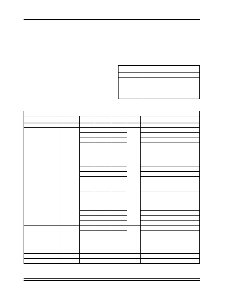
PIN FUNCTION TABLE
DC CHARACTERISTICS
Symbol
Description
V
OUT
Digital Output
V
IN
Analog Input
V
SS
Ground Terminal
NC
No Connect
NC
No Connect
Electrical Specifications: Unless otherwise noted, T
A
= +25∞C.
Parameter
Sym
Min
Typ
Max
Units
Test Conditions
Operating Voltage
V
IN
0.7
--
10.0
V
(V
DET
-) = 0.8 to 6.0V
Quiescent Current
I
SS
--
0.8
2.7
µA
V
IN
= 2.0V
--
0.9
3.0
V
IN
= 3.0V
--
1.0
3.2
V
IN
= 4.0V
--
1.1
3.6
V
IN
= 5.0V
Threshold Voltage
Note 1
V
DET -
1.37
1.4
1.43
V
TC54VX14
2.06
2.1
2.14
TC54VX21
2.65
2.7
2.75
TC54VX27
2.84
2.9
2.96
TC54VX29
2.94
3.0
3.06
TC54VX30
4.12
4.2
4.28
TC54VX42
4.21
4.3
4.39
TC54VX43
7.54
7.7
7.86
TC54VX77 (5-pin SOT-23A only)
Hysteresis Voltage
V
HYST
28
70
112
mV
V
DET
= 1.4V (typ)
42
105
168
V
DET
= 2.1V (typ)
54
135
216
V
DET
= 2.7V (typ)
58
145
232
V
DET
= 2.9V (typ)
60
150
240
V
DET
= 3.0V (typ)
84
210
336
V
DET
= 4.2V (typ)
86
215
344
V
DET
= 4.3V (typ)
154
385
616
V
DET
= 7.7V (typ)
Output Current
I
OUT
--
7.7
--
mA
V
OL
= 0.5V, V
IN
= 2.1V
--
10.1
--
V
IN
= 3.0V
--
11.5
--
V
IN
= 4.0V
--
13.0
--
V
IN
= 5.0V
--
-10.0
--
TC54VC Only:
V
OH
= V
IN
≠ 2.1V, V
IN
= 8.0V
Tempco of (V
DET
-)
T
C
(V
DET
-)
--
±100
--
ppm/∞C -40∞C
T
A
85∞C
Delay Time
t
DLY
--
--
0.2
ms
V
DET
-
V
OUT
inversion
Note 1:
For other voltage options, please contact your regional Microchip sales office.
2003 Microchip Technology Inc.
DS21434E-page 3
TC54
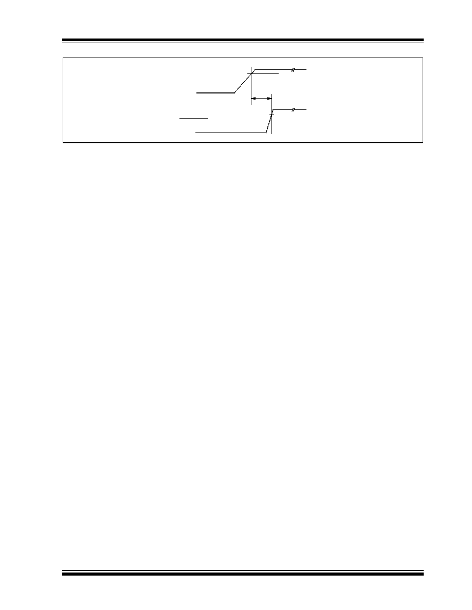
FIGURE 1-1:
Timing Diagram.
V
DD
OUTPUT
V
OH
t
DLY
V
DET-
OUTPUT

TC54
DS21434E-page 4
2003 Microchip Technology Inc.
2.0
PIN DESCRIPTIONS
The descriptions of the pins are listed in Table 2-1.
TABLE 2-1:
PIN FUNCTION TABLE
2.1
Digital Output (V
OUT
)
V
OUT
goes low when V
IN
drops below V
DET -
and
returns high when V
IN
rises above V
DET -
+ V
HYST
. (See
Figure 3-1, "Timing Diagram".)
2.2
Analog Input (V
IN
)
V
IN
can be used for power supply monitoring or a
voltage level that requires monitoring.
2.3
Ground Terminal (V
SS
)
V
SS
provides the negative reference for the analog
input voltage. Typically, the circuit ground is used.
2.4
No Connect (NC)
No internal connection.
Pin No.
(3-Pin SOT-23A)
Pin No.
(3-Pin SOT-89)
(3-Pin TO-92)
Pin No.
(5-Pin SOT-23A)
Symbol
Description
1
1
1
V
OUT
Digital Output
3
2
2
V
IN
Analog Input
2
3
3
V
SS
Ground Terminal
--
--
4
NC
No Connect
--
--
5
NC
No Connect

2003 Microchip Technology Inc.
DS21434E-page 5
TC54
3.0
DETAILED DESCRIPTION
In normal steady-state operation when V
IN
> V
DET-
,
the output will be at a logic-high (see Figure 3-1). In
the case of the TC54VN, this is an open-drain condi-
tion. If and when the input falls below V
DET -
, the output
will pull down (Logic 0) to V
SS
. Generally, V
OUT
can
pull down to within 0.5V of V
SS
at rated output current
and input voltage. (See Section 1.0, "Electrical
Characteristics").
The output (V
OUT
) will stay valid until the input voltage
falls below the minimum operating voltage (V
INMIN
) of
0.7V. Below this minimum operating voltage, the output
is undefined. During power-up (or anytime V
IN
has
fallen below V
INMIN
), V
OUT
will remain undefined until
V
IN
rises above V
INMIN
. Once this occurs, the output
will become valid. V
OUT
will be in its active-low state,
while V
INMIN
< V
IN
< V
DET+
(therefore, V
DET+
= V
DET-
+ V
HYST
). If and when the input rises above V
DET +
, the
output will assume its inactive state (high for TC54VC,
open-drain for TC54VN).
FIGURE 3-1:
Timing Diagram.
V
IN
Detect Voltage V
DET
-
Minimum Operating
Voltage
V
HYST
V
DET+
Output Voltage
Release Voltage
or RESET Voltage
Ground Level
Ground Level
V
OUT