2002 Microchip Technology Inc.
DS21447C-page 1
M
TC647
Features
· Temperature Proportional Fan Speed for Acoustic
Control and Longer Fan Life
· Efficient PWM Fan Drive
· 3.0V to 5.5V Supply Range:
- Fan Voltage Independent of TC647
Supply Voltage
- Supports any Fan Voltage
· FanSenseTM
Technology Fault Detection Circuits
Protect Against Fan Failure and Aid System
Testing
· Shutdown Mode for "Green" Systems
· Supports Low Cost NTC/PTC Thermistors
· Space Saving 8-Pin MSOP Package
Applications
· Power Supplies
· Personal Computers
· File Servers
· Telecom Equipment
· UPSs, Power Amps
· General Purpose Fan Speed Control
Available Tools
· Fan Controller Demonstration Board (TC642DEMO)
· Fan Controller Evaluation Kit (TC642EV)
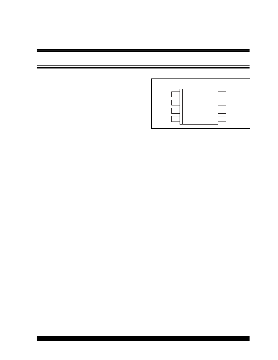
Package Types
General Description
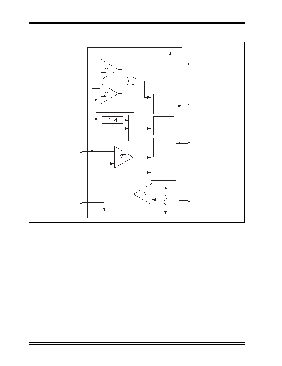
The TC647 is a switch mode, fan speed controller for
use with brushless DC fans. Temperature proportional
speed control is accomplished using pulse width mod-
ulation (PWM). A thermistor (or other voltage output
temperature sensor) connected to V
IN
furnishes the
required control voltage of 1.25V to 2.65V (typical) for
0% to 100% PWM duty cycle. Minimum fan speed is
set by a simple resistor divider on the V
MIN
input. An
integrated Start-up Timer ensures reliable motor start-
up at turn-on, coming out of shutdown mode or
following a transient fault. A logic low applied to V
MIN
(Pin 3) causes fan shutdown.
The TC647 also features Microchip Technology's pro-
prietary FanSenseTM technology for increasing system
reliability. In normal fan operation, a pulse train is
present at SENSE (Pin 5). A missing pulse detector
monitors this pin during fan operation. A stalled, open
or unconnected fan causes the TC647 to trigger its
Start-up Timer once. If the fault persists, the FAULT
output goes low and the device is latched in its shut-
down mode.
The TC647 is available in the 8-pin plastic DIP, SOIC
and MSOP packages and is available in the industrial
and extended commercial temperature ranges.
1
8
2
7
3
6
4
5
TC647
GND
C
F
V
IN
V
MIN
FAULT
SENSE
V
DD
V
OUT
SOIC/PDIP/MSOP
PWM Fan Speed Controller with FanSense
TM
Technology
2002 Microchip Technology Inc.
DS21447C-page 3
TC647
1.0
ELECTRICAL
CHARACTERISTICS
Absolute Maximum Ratings*
Supply Voltage ......................................................... 6V
Input Voltage, Any Pin.... (GND 0.3V) to (V
DD
+0.3V)
Package Thermal Resistance:
PDIP (R
JA
)............................................. 125°C/W
SOIC (R
JA
) ............................................155°C/W
MSOP (R
JA
) .......................................... 200°C/W
Specified Temperature Range ........... -40°C to +125°C
Storage Temperature Range.............. -65°C to +150°C
*Stresses above those listed under "Absolute Maximum Rat-
ings" may cause permanent damage to the device. These are
stress ratings only and functional operation of the device at
these or any other conditions above those indicated in the
operation sections of the specifications is not implied. Expo-
sure to absolute maximum rating conditions for extended peri-
ods may affect device reliability.
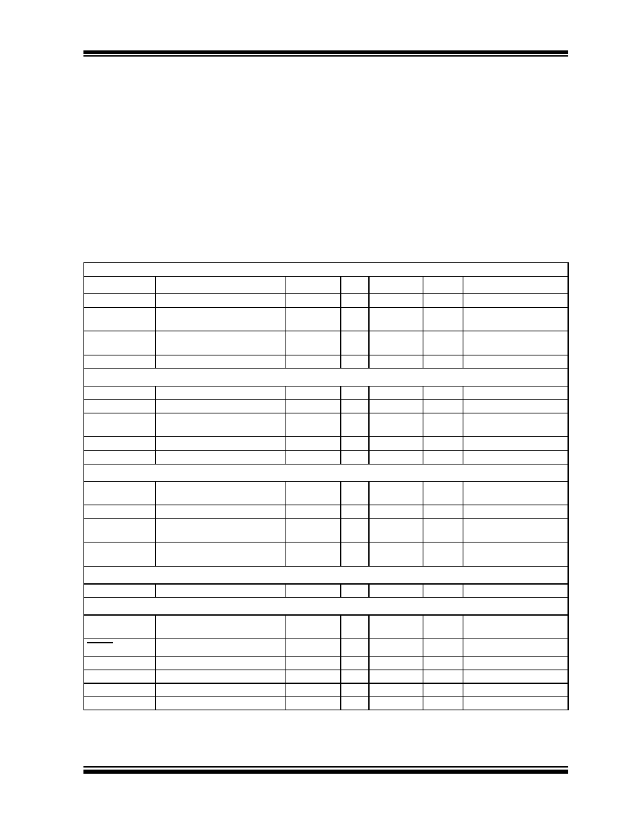
DC ELECTRICAL SPECIFICATIONS
Electrical Characteristics: Unless otherwise specified, T
MIN
< T
A
< T
MAX
, V
DD
= 3.0V to 5.5V.
Symbol
Parameter
Min
Typ
Max
Units
Test Conditions
V
DD
Supply Voltage
3.0
--
5.5
V
I
DD
Supply Current, Operating
--
0.5
1
mA
Pins 6, 7 Open,
C
F
= 1 µF, V
IN
= V
C(MAX)
I
DD(SHDN)
Supply Current,
Shutdown Mode
--
25
--
µA
Pins 6, 7 Open,
C
F
= 1 µF, V
MIN
= 0.35V
I
IN
V
IN
,
V
MIN
Input Leakage
1.0
--
+1.0
µA
Note 1
V
OUT
Output
t
R
V
OUT
Rise Time
--
--
50
µsec
I
OH
= 5 mA, Note 1
t
F
V
OUT
Fall Time
--
--
50
µsec
I
OL
= 1 mA, Note 1
t
SHDN
Pulse Width (On V
MIN
) to Clear
Fault Mode
30
--
--
µsec
V
SHDN
, V
HYST
Specifications, Note 1
I
OL
Sink Current at V
OUT
Output
1.0
--
--
mA
V
OL
= 10% of V
DD
I
OH
Source Current at V
OUT
Output
5.0
--
--
mA
V
OH
= 80% of V
DD
V
IN
, V
MIN
Inputs
V
C(MAX)
Input Voltage at V
IN
or V
MIN
for
100% PWM Duty Cycle
2.5
2.65
2.8
V
V
C(SPAN)
V
C(MAX)
- V
C(MIN)
1.3
1.4
1.5
V
V
SHDN
Voltage Applied to V
MIN
to
Ensure Shutdown Mode
--
--
V
DD
x 0.13
V
V
REL
Voltage Applied to V
MIN
to
Release Shutdown Mode
V
DD
x 0.19
--
--
V
V
DD
= 5V
Pulse Width Modulator
F
PWM
PWM Frequency
26
30
34
Hz
C
F
= 1.0 µF
SENSE Input
V
TH(SENSE)
SENSE Input Threshold
Voltage with Respect to GND
50
70
90
mV
Note 1
FAULT Output
V
OL
Output Low Voltage
--
--
0.3
V
I
OL
= 2.5 mA
t
MP
Missing Pulse Detector Timer
--
32/F
--
Sec
t
STARTUP
Start-up Timer
--
32/F
--
Sec
t
DIAG
Diagnostic Timer
--
3/F
--
Sec
Note 1: Ensured by design, not tested.
TC647
DS21447C-page 4
2002 Microchip Technology Inc.
2.0
PIN DESCRIPTIONS
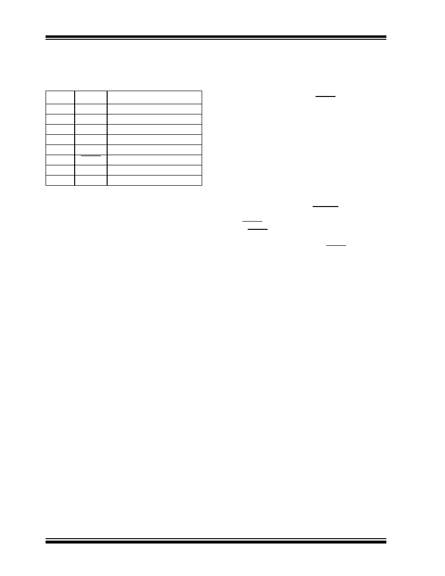
The descriptions of the pins are listed in Table 2-1.
TABLE 2-1:
PIN FUNCTION TABLE
2.1
Analog Input (V
IN
)
The thermistor network (or other temperature sensor)
connects to the V
IN
input. A voltage range of 1.25V to
2.65V (typical) on this pin drives an active duty cycle of
0% to 100% on the V
OUT
pin.
2.2
Analog Output (C
F
)
C
F
is the positive terminal for the PWM ramp generator
timing capacitor. The recommended C
F
is 1 µF for
30 Hz PWM operation.
2.3
Analog Input (V
MIN
)
An external resistor divider connected to the V
MIN
input
sets the minimum fan speed by fixing the minimum
PWM duty cycle (1.25V to 2.65V = 0% to 100%, typi-
cal). The TC647 enters shutdown mode when V
MIN
V
SHDN
. During shutdown, the FAULT output is inactive
and supply current falls to 25 µA (typical). The TC647
exits shutdown mode when V
MIN
V
REL
. See
Section 5.0, "Typical Applications", for more details.
2.4
Ground (GND)
GND denotes the ground terminal.
2.5
Analog Input (SENSE)
Pulses are detected at the SENSE pin as fan rotation
chops the current through a sense resistor. The
absence of pulses indicates a fault.
2.6
Digital Output (FAULT)
The FAULT line goes low to indicate a fault condition.
When FAULT goes low due to a fan fault condition, the
device is latched in shutdown mode until deliberately
cleared or until power is cycled. FAULT may be con-
nected to V
MIN
if a hard shutdown is desired.
2.7
Digital Output (V
OUT
)
V
OUT
is an active high complimentary output that drives
the base of an external NPN transistor (via an appropri-
ate base resistor) or the gate of an N-channel MOS-
FET. This output has asymmetrical drive (see
Section 1.0, "Electrical Characteristics").
2.8
Power Supply Input (V
DD
)
V
DD
may be independent of the fan's power supply
(see Section 1.0, "Electrical Characteristics").
Pin No.
Symbol
Description
1
V
IN
Analog Input
2
C
F
Analog Output
3
V
MIN
Analog Input
4
GND
Ground Terminal
5
SENSE
Analog Input
6
FAULT
Digital (Open Collector) Output
7
V
OUT
Digital Output
8
V
DD
Power Supply Input
2002 Microchip Technology Inc.
DS21447C-page 5
TC647
3.0
DETAILED DESCRIPTION
3.1
PWM
The PWM circuit consists of a ramp generator and
threshold detector. The frequency of the PWM is deter-
mined by the value of the capacitor connected to the C
F
input. A frequency of 30 Hz is recommended
(C
F
= 1 µF). The PWM is also the time base for the
Start-up Timer (see Section 3.3, "Start-Up Timer"). The
PWM voltage control range is 1.25V to 2.65V (typical)
for 0% to 100% output duty cycle.
3.2
V
OUT
Output
The V
OUT
pin is designed to drive a low cost transistor
or MOSFET as the low side power switching element in
the system. Various examples of driver circuits will be
shown throughout this data sheet. This output has an
asymmetric complimentary drive and is optimized for
driving NPN transistors or N-channel MOSFETs. Since
the system relies on PWM rather than linear control,
the power dissipation in the power switch is kept to a
minimum. Generally, very small devices (TO-92 or SOT
packages) will suffice.
3.3
Start-Up Timer
To ensure reliable fan start-up, the Start-up Timer turns
the V
OUT
output on for 32 cycles of the PWM whenever
the fan is started from the off state. This occurs at
power up and when coming out of shutdown mode. If
the PWM frequency is 30 Hz (C
F
= 1 µF), the resulting
start-up time will be approximately one second. If a
fault is detected, the Diagnostic Timer is triggered
once, followed by the Start-up Timer. If the fault
persists, the device is shut down (see Section 3.6,
"FAULT Output").
3.4
Shutdown Control (Optional)
If V
MIN
(Pin 3) is pulled below V
SHDN
, the TC647 will go
into shutdown mode. This can be accomplished by
driving V
MIN
with an open-drain logic signal or using an
external transistor, as shown in Figure 3-1. All functions
are suspended until the voltage on V
MIN
becomes
higher than V
REL
(0.85V @ V
DD
= 5.0V). Pulling V
MIN
below V
SHDN
will always result in complete device
shutdown and reset. The FAULT output is
unconditionally inactive in shutdown mode.
A small amount of hysteresis, typically one percent of
V
DD
(50 mV at V
DD
= 5.0V), is designed into the V
SHDN
/
V
REL
threshold. The levels specified for V
SHDN
and
V
REL
in Section 1.0, "Electrical Characteristics",
include this hysteresis plus adequate margin to
account for normal variations in the absolute value of
the threshold and hysteresis.
3.5
SENSE Input
(FanSense
TM
Technology)
The SENSE input (Pin 5) is connected to a low value
current sensing resistor in the ground return leg of the
fan circuit. During normal fan operation, commutation
occurs as each pole of the fan is energized. This
causes brief interruptions in the fan current, seen as
pulses across the sense resistor. If the device is not in
shutdown mode, and pulses are not appearing at the
SENSE input, a fault exists.
The short, rapid change in fan current (high dI/dt)
causes a corresponding dV/dt across the sense
resistor, R
SENSE
. The waveform on R
SENSE
is
differentiated and converted to a logic-level, pulse-train
by C
SENSE
and the internal signal processing circuitry.
The presence and frequency of this pulse-train is a
direct indication of fan operation. See Section 5.0,
"Typical Applications", for more details.
3.6
FAULT Output
Pulses appearing at SENSE due to the PWM turning
on are blanked with the remaining pulses being filtered
by a missing pulse detector. If consecutive pulses are
not detected for 32 PWM cycles (
1 Sec if C
F
= 1 µF),
the Diagnostic Timer is activated and V
OUT
is driven
high continuously for three PWM cycles (
100 msec if
C
F
= 1 µF). If a pulse is not detected within this window,
the Start-up Timer is triggered (see Section 3.3, "Start-
Up Timer"). This should clear a transient fault condition.
If the missing pulse detector times out again, the PWM
is stopped and FAULT goes low. When FAULT is
activated due to this condition, the device is latched in
shutdown mode and will remain off indefinitely.
The TC647 may be configured to continuously attempt
fan restarts, if so desired.
CAUTION: Shutdown mode is unconditional. That is,
the fan will not be activated regardless of the voltage
at V
IN
. The fan should not be shut down until all heat
producing activity in the system is at a negligible
level.
Note:
At this point, action must be taken to restart
the fan by momentarily pulling V
MIN
below
V
SHDN
, or cycling system power. In either
case, the fan cannot remain disabled due
to a fault condition as severe system dam-
age could result. If the fan cannot be
restarted, the system should be shut down.