 | ÐлекÑÑоннÑй компоненÑ: TC648BEOA | СкаÑаÑÑ:  PDF PDF  ZIP ZIP |
PWM Fan Speed Controllers With Auto-Shutdown, Fan Restart and FanSense Technology for Fault Detection
2003 Microchip Technology Inc.
DS21755B-page 1
M
TC646B/TC648B/TC649B
Features
· Temperature-Proportional Fan Speed for Acoustic
Noise Reduction and Longer Fan Life
· Efficient PWM Fan Drive
· 3.0V to 5.5V Supply Range:
- Fan Voltage Independent of TC646B/
TC648B/TC649B Supply Voltage
- Supports any Fan Voltage
· FanSense
TM
Fault Detection Circuit Protects
Against Fan Failure and Aids System Testing
(TC646B/TC649B)
· Automatic Shutdown Mode for "Green" Systems
· Supports Low Cost NTC/PTC Thermistors
· Over-Temperature Indication (TC646B/TC648B)
· Fan Auto-Restart
· Space-Saving 8-Pin MSOP Package
Applications
· Personal Computers & Servers
· LCD Projectors
· Datacom & Telecom Equipment
· Fan Trays
· File Servers
· General-Purpose Fan Speed Control
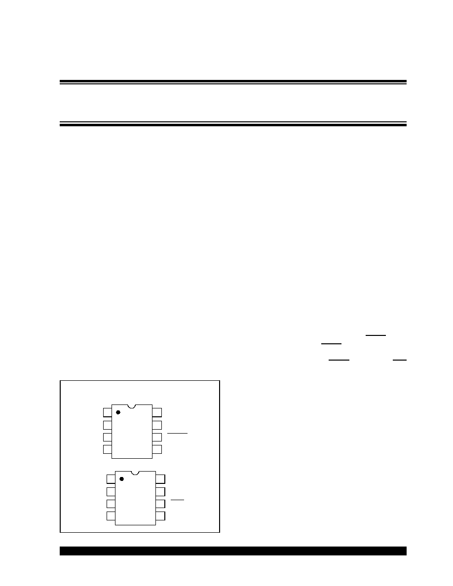
Package Types
Description
The TC646B/TC648B/TC649B devices are new ver-
sions of the existing TC646/TC648/TC649 fan speed
controllers. These devices are switch-mode fan speed
controllers that incorporate a new fan auto-restart func-
tion. Temperature-proportional speed control is accom-
plished using pulse width modulation. A thermistor (or
other voltage output temperature sensor) connected to
the V
IN
input supplies the required control voltage of
1.20V to 2.60V (typical) for 0% to 100% PWM duty
cycle. The auto-shutdown threshold/temperature is set
by a simple resistor divider on the V
AS
input. An inte-
grated Start-Up Timer ensures reliable fan motor start-
up at turn-on, coming out of shutdown mode, auto-
shutdown mode or following a transient fault. A logic
low applied to V
IN
(pin 1) causes fan shutdown.
The TC646B and TC649B also feature Microchip
Technology's proprietary FanSense technology for
increasing system reliability. In normal fan operation, a
pulse train is present at SENSE (pin 5). A missing-
pulse detector monitors this pin during fan operation. A
stalled, open or unconnected fan causes the TC646B/
TC649B device to turn the V
OUT
output on full (100%
duty cycle). If the fan fault persists (a fan current pulse
is not detected within a 32/f period), the FAULT output
goes low. Even with the FAULT output low, the V
OUT
output is on full during the fan fault condition in order to
attempt to restart the fan. FAULT (TC646B) or OTF
(TC648B) is also asserted if the PWM reaches 100%
duty cycle, indicating that maximum cooling capability
has been reached and a possible overheating condition
exists.
The TC646B, TC648B and TC649B devices are avail-
able in 8-pin plastic MSOP, SOIC and PDIP packages.
The specified temperature range of these devices is
-40 to +85ºC.
MSOP, PDIP, SOIC
1
2
3
4
V
DD
5
6
7
8
V
OUT
SENSE
V
IN
C
F
V
AS
GND
FAULT
TC646B
TC649B
1
2
3
4
V
DD
5
6
7
8
V
OUT
NC
V
IN
C
F
V
AS
GND
OTF
TC648B
PWM Fan Speed Controllers With Auto-Shutdown, Fan
Restart and FanSenseTM Technology for Fault Detection
TC646B/TC648B/TC649B
DS21755B-page 2
2003 Microchip Technology Inc.
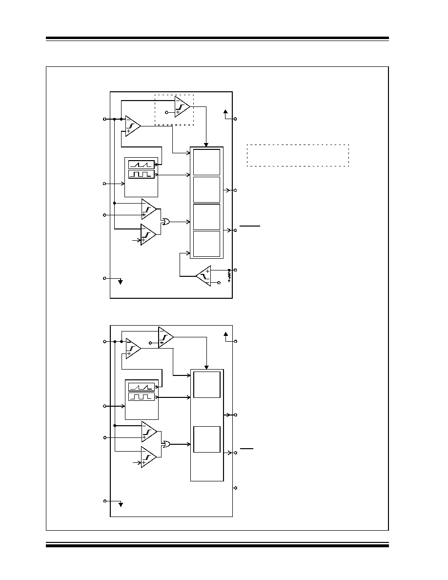
Functional Block Diagram
TC646B/TC649B
Note: The V
OTF
comparator
is for the TC646B device only.
70 mV
(typ)
V
OTF
10 k
V
SHDN
V
IN
C
F
V
AS
GND
V
DD
V
OUT
FAULT
SENSE
Clock
Generator
Control
Logic
3xT
PWM
Timer
Start-up
Timer
Missing
Pulse
Detect
TC648B
V
OTF
V
SHDN
V
IN
C
F
V
AS
GND
V
DD
V
OUT
OTF
NC
Clock
Generator
Control
Logic
Start-up
Timer
Note
2003 Microchip Technology Inc.
DS21755B-page 3
TC646B/TC648B/TC649B
1.0
ELECTRICAL
CHARACTERISTICS
Absolute Maximum Ratings
Supply Voltage (V
DD
) .......................................................6.0V
Input Voltage, Any Pin................(GND - 0.3V) to (V
DD
+0.3V)
Operating Temperature Range ....................- 40°C to +125°C
Maximum Junction Temperature, T
J
........................... +150°C
ESD Protection on all pins ........................................... > 3 kV
Notice: Stresses above those listed under "Maximum
Ratings" may cause permanent damage to the device. This is
a stress rating only and functional operation of the device at
those or any other conditions above those indicated in the
operational listings of this specification is not implied. Expo-
sure to maximum rating conditions for extended periods may
affect device reliability.
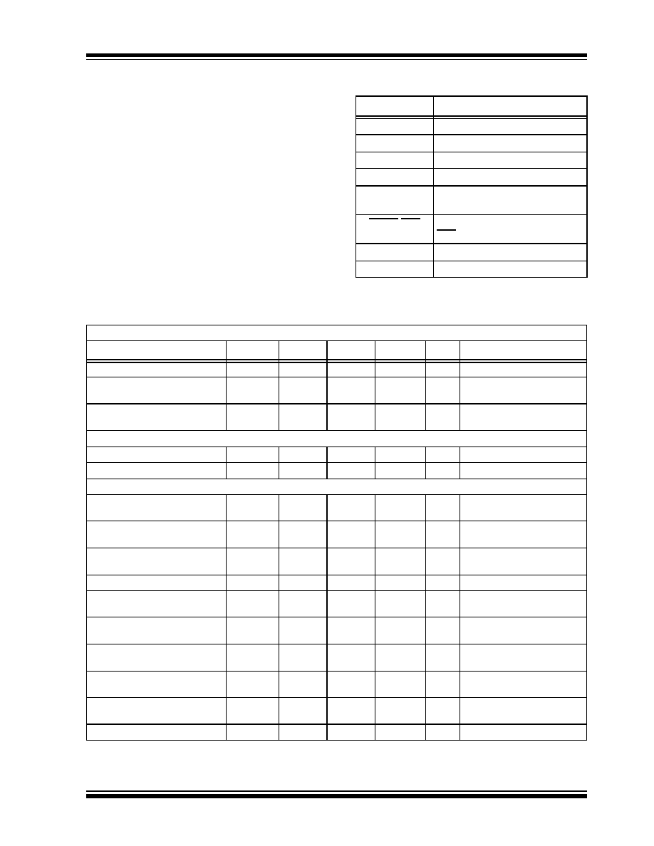
PIN FUNCTION TABLE
Name
Function
V
IN
Analog Input
C
F
Analog Output
V
AS
Analog Input
GND
Ground
SENSE/NC
Analog Input.
No Connect (NC) for TC648B
FAULT/OTF
Digital (Open-Drain) Output
OTF for TC648B
V
OUT
Digital Output
V
DD
Power Supply Input
ELECTRICAL CHARACTERISTICS
Electrical Specifications: Unless otherwise specified, all limits are specified for -40°C < T
A
< +85°C, V
DD
= 3.0V to 5.5V.
Parameters
Sym
Min
Typ
Max
Units
Conditions
Supply Voltage
V
DD
3.0
--
5.5
V
Supply Current, Operating
I
DD
--
200
400
µA
Pins 6, 7 Open,
C
F
= 1 µF, V
IN
= V
C(MAX)
Supply Current, Shutdown Mode
I
DD(SHDN)
--
30
--
µA
Pins 6, 7 Open,
C
F
= 1 µF, V
IN
= 0.35V
V
OUT
Output
Sink Current at V
OUT
Output
I
OL
1.0
--
--
mA
V
OL
= 10% of V
DD
Source Current at V
OUT
Output
I
OH
5.0
--
--
mA
V
OH
= 80% of V
DD
V
IN
, V
AS
Inputs
Input Voltage at V
IN
for 100% PWM
Duty Cycle
V
C(MAX)
2.45
2.60
2.75
V
Over-Temperature Indication
Threshold
V
OTF
V
C(MAX)
+
20 mV
V
For TC646B and TC648B
Over-Temperature Indication
Threshold Hysteresis
V
OTF-HYS
80
mV
For TC646B and TC648B
V
C(MAX)
- V
C(MIN)
V
C(SPAN)
1.3
1.4
1.5
V
Hysteresis on Auto-Shutdown
Comparator
V
HAS
--
70
--
mV
Auto-Shutdown Threshold
V
AS
V
C(MAX)
-
V
C(SPAN)
--
V
C(MAX)
V
Voltage Applied to V
IN
to Ensure
Shutdown Mode
V
SHDN
--
--
V
DD
x 0.13
V
Voltage Applied to V
IN
to Release
Shutdown Mode
V
REL
V
DD
x 0.19
--
--
V
V
DD
= 5V
Hysteresis on V
SHDN
, V
REL
V
HYST
--
0.03 X
V
DD
--
V
V
IN
,
V
AS
Input Leakage
I
IN
- 1.0
--
+1.0
µA
Note 1
Note 1:
Ensured by design, tested during characterization.
2:
For V
DD
< 3.7V, t
STARTUP
and t
MP
timers are typically 13/f.
TC646B/TC648B/TC649B
DS21755B-page 4
2003 Microchip Technology Inc.
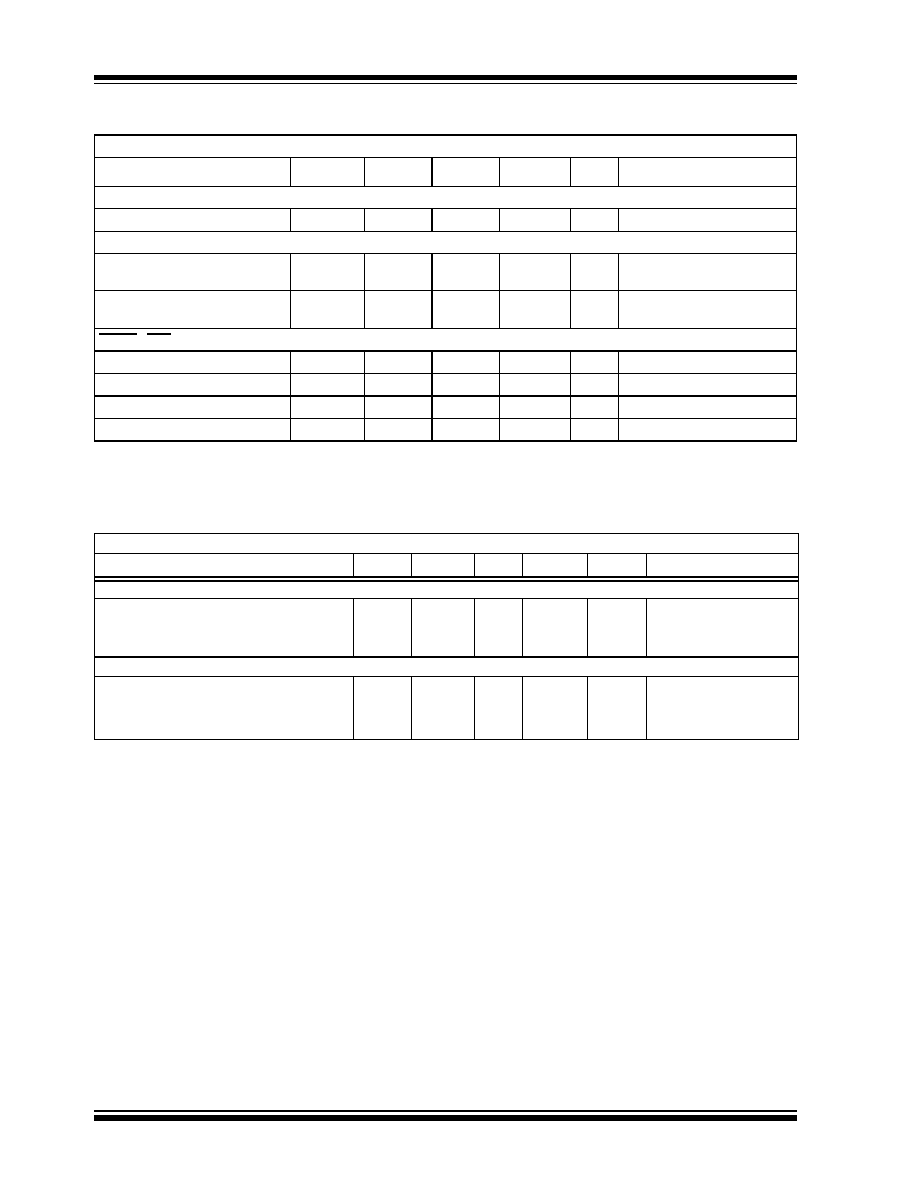
TEMPERATURE SPECIFICATIONS
Pulse-Width Modulator
PWM Frequency
f
PWM
26
30
34
Hz
C
F
= 1.0 µF
SENSE Input (TC646B & TC649B)
SENSE Input Threshold Voltage
with Respect to GND
V
TH(SENSE)
50
70
90
mV
Blanking time to ignore pulse due
to V
OUT
turn-on
t
BLANK
--
3.0
--
µsec
FAULT / OTF Output
Output Low Voltage
V
OL
--
--
0.3
V
I
OL
= 2.5 mA
Missing Pulse Detector Timer
t
MP
--
32/f
--
sec
TC646B and TC649B, Note 2
Start-up Timer
t
STARTUP
--
32/f
--
sec
Note 2
Diagnostic Timer
t
DIAG
--
3/f
--
sec
TC646B and TC649B
ELECTRICAL CHARACTERISTICS (CONTINUED)
Electrical Specifications: Unless otherwise specified, all limits are specified for -40°C < T
A
< +85°C, V
DD
= 3.0V to 5.5V.
Parameters
Sym
Min
Typ
Max
Units
Conditions
Note 1:
Ensured by design, tested during characterization.
2:
For V
DD
< 3.7V, t
STARTUP
and t
MP
timers are typically 13/f.
Electrical Characteristics: Unless otherwise noted, all parameters apply at V
DD
= 3.0V to 5.5V
Parameters
Sym
Min
Typ
Max
Units
Conditions
Temperature Ranges
Specified Temperature Range
T
A
-40
--
+85
°C
Operating Temperature Range
T
A
-40
--
+125
°C
Storage Temperature Range
T
A
-65
--
+150
°C
Thermal Package Resistances
Thermal Package Resistance, 8-Pin MSOP
JA
--
200
--
°C/W
Thermal Package Resistance, 8-Pin SOIC
JA
--
155
--
°C/W
Thermal Package Resistance, 8-Pin PDIP
JA
--
125
--
°C/W
2003 Microchip Technology Inc.
DS21755B-page 5
TC646B/TC648B/TC649B
TIMING SPECIFICATIONS
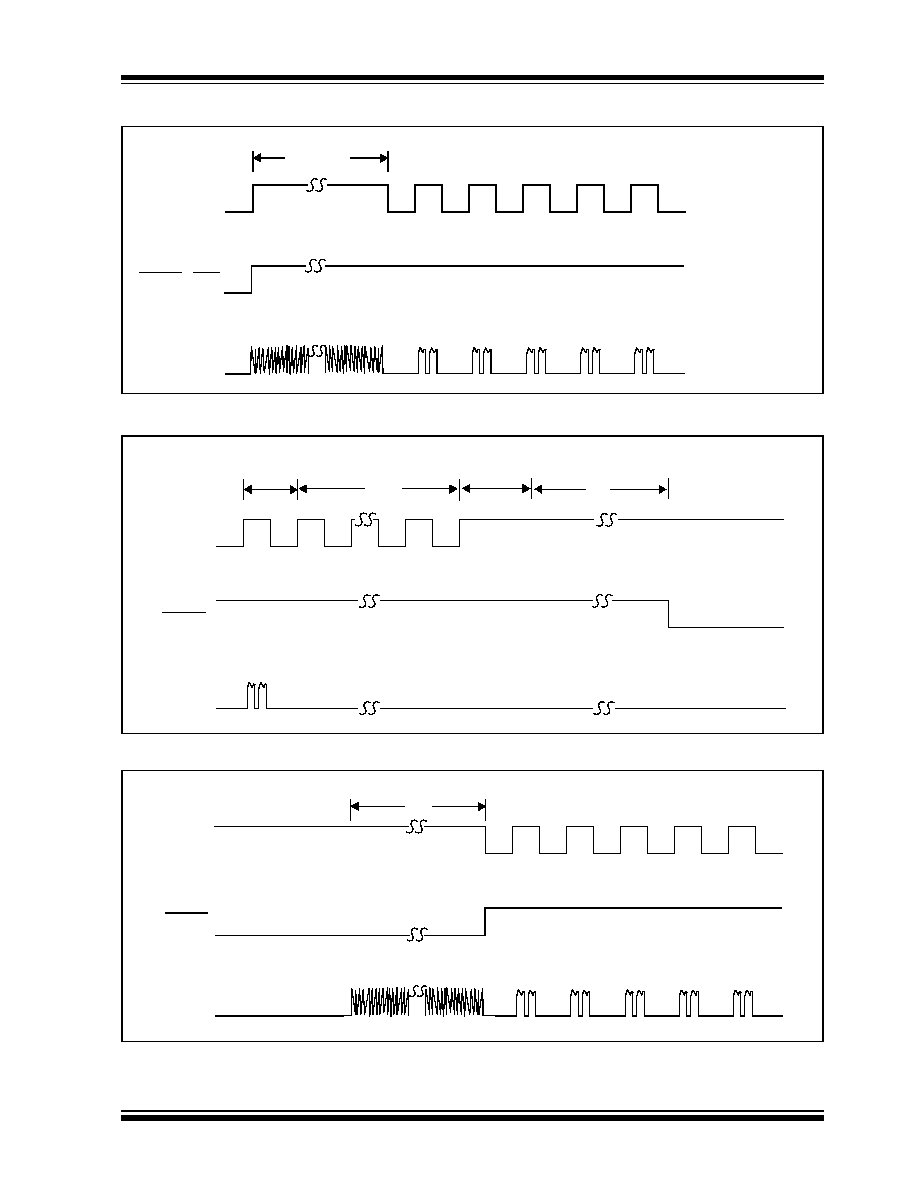
FIGURE 1-1:
TC646B/TC648B/TC649B Start-up Timing.
FIGURE 1-2:
Fan Fault Occurrence (TC646B and TC649B).
FIGURE 1-3:
Recovery From Fan Fault (TC646B and TC649B).
V
OUT
FAULT / OTF
SENSE
t
STARTUP
(TC646B and TC649B)
V
OUT
FAULT
SENSE
33.3 msec (C
F
= 1 µF)
t
MP
t
MP
t
DIAG
V
OUT
FAULT
SENSE
Minimum 16 pulses
t
MP
TC646B/TC648B/TC649B
DS21755B-page 6
2003 Microchip Technology Inc.
FIGURE 1-4:
TC646B/TC648B/TC649B Electrical Characteristics Test Circuit.
1
2
3
4
6
5
7
8
V
IN
C
F
V
AS
GND
FAULT / OTF
SENSE
V
OUT
V
DD
R
3
R
1
C
3
0.1 µF
C
2
1 µF
V
DD
C
1
0.1 µF
+
-
V
IN
+
-
C
4
0.1 µF
V
AS
+
-
R
2
K
1
K
2
0.1 µF
1 µF
.01 µF
C
7
C
6
C
5
R
4
V
SENSE
(pulse voltage source)
K
4
K
3
+
-
Current
limited
voltage
source
V
DD
R
5
Current
limited
voltage
source
C
8
0.1 µF
R
6
Note: C
5
and C
7
are adjusted to get the necessary 1 µF value.
TC646B and TC649B
TC646B
TC648B
TC649B
+
-
2003 Microchip Technology Inc.
DS21755B-page 7
TC646B/TC648B/TC649B
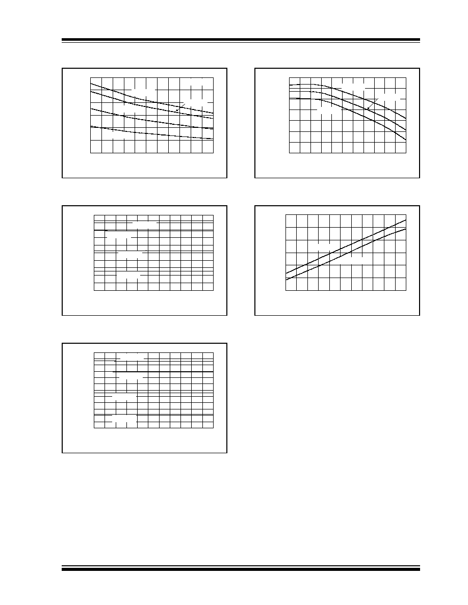
2.0
TYPICAL PERFORMANCE CURVES
Note: Unless otherwise indicated, V
DD
= 5V, T
A
= 25°C.
FIGURE 2-1:
I
DD
vs. Temperature.
FIGURE 2-2:
PWM Sink Current (I
OL
) vs.
V
OL
.
FIGURE 2-3:
PWM Source Current (I
OH
)
vs. V
DD
- V
OH
.
FIGURE 2-4:
PWM Frequency vs.
Temperature.
FIGURE 2-5:
I
DD
vs. V
DD
.
FIGURE 2-6:
I
DD
Shutdown vs.
Temperature.
Note:
The graphs and tables provided following this note are a statistical summary based on a limited number of
samples and are provided for informational purposes only. The performance characteristics listed herein
are not tested or guaranteed. In some graphs or tables, the data presented may be outside the specified
operating range (e.g., outside specified power supply range) and therefore outside the warranted range.
125
130
135
140
145
150
155
160
165
-40 -25 -10
5
20
35
50
65
80
95 110 125
Temperature (ºC)
I
DD
(µA)
V
DD
= 3.0V
V
DD
= 5.5V
Pins 6 & 7 Open
C
F
= 1 µF
0
2
4
6
8
10
12
14
16
0
50 100 150 200 250 300 350 400 450 500 550 600
V
OL
(mV)
I
OL
(mA)
V
DD
= 5.5V
V
DD
= 5.0V
V
DD
= 3.0V
V
DD
= 4.0V
0
2
4
6
8
10
12
14
16
0
100
200
300
400
500
600
700
800
V
DD
- V
OH
(mV)
I
OH
(mA)
V
DD
= 5.5V
V
DD
= 5.0V
V
DD
= 3.0V
V
DD
= 4.0V
28.50
29.00
29.50
30.00
30.50
-40 -25 -10
5
20
35
50
65
80
95 110 125
Temperature (ºC)
Oscillator Frequency (Hz)
V
DD
= 3.0V
V
DD
= 5.5V
C
F
= 1.0 F
125
130
135
140
145
150
155
160
165
170
3
3.5
4
4.5
5
5.5
V
DD
(V)
I
DD
(µA)
T
A
= -40ºC
T
A
= -5ºC
T
A
= +125ºC
T
A
= +90ºC
Pins 6 & 7 Open
C
F
= 1 µF
15
18
21
24
27
30
-40 -25 -10
5
20
35
50
65
80
95
110 125
Temperature (ºC)
I
DD
Shutdown (µA)
V
DD
= 5.5V
V
DD
= 3.0V
Pins 6 & 7 Open
V
IN
= 0V
TC646B/TC648B/TC649B
DS21755B-page 8
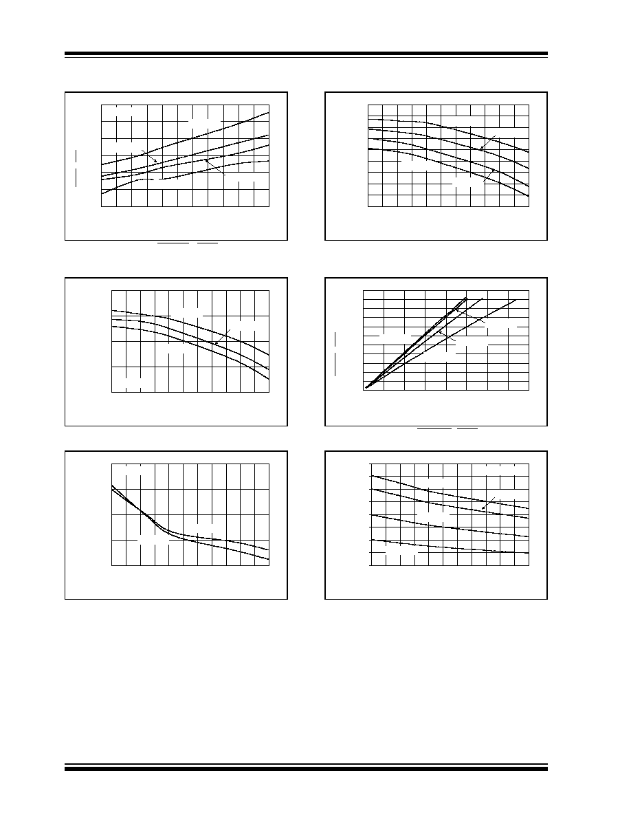
2003 Microchip Technology Inc.
Note: Unless otherwise indicated, V
DD
= 5V, T
A
= 25°C.
FIGURE 2-7:
FAULT / OTF V
OL
vs.
Temperature.
FIGURE 2-8:
V
C(MAX)
vs. Temperature.
FIGURE 2-9:
V
C(MIN)
vs. Temperature.
FIGURE 2-10:
Sense Threshold
(V
TH(SENSE)
) vs. Temperature.
FIGURE 2-11:
FAULT / OTF I
OL
vs. V
OL
.
FIGURE 2-12:
PWM Source Current (I
OH
)
vs. Temperature.
10
20
30
40
50
60
70
-40 -25 -10
5
20
35
50
65
80
95
110 125
Temperature (ºC)
FAULT / OTF V
OL
(mV)
I
OL
= 2.5 mA
V
DD
= 3.0V
V
DD
= 5.5V
V
DD
= 5.0V
V
DD
= 4.0V
2.570
2.580
2.590
2.600
2.610
-40 -25 -10
5
20
35
50
65
80
95 110 125
Temperature (ºC)
V
C(MAX)
(V)
V
DD
= 5.0V
V
DD
= 5.5V
V
DD
= 3.0V
C
F
= 1 µF
1.180
1.190
1.200
1.210
1.220
-40 -25 -10
5
20
35
50
65
80
95 110 125
Temperature (ºC)
V
C(MIN)
(V)
V
DD
= 5.0V
V
DD
= 3.0V
C
F
= 1 µF
69.5
70.0
70.5
71.0
71.5
72.0
72.5
73.0
73.5
74.0
-40 -25 -10
5
20
35
50
65
80
95 110 125
Temperature (ºC)
V
TH(SENSE)
(mV)
V
DD
= 3.0V
V
DD
= 4.0V
V
DD
= 5.5V
V
DD
= 5.0V
0
2
4
6
8
10
12
14
16
18
20
22
0
50
100
150
200
250
300
350
400
V
OL
(mV)
FAULT / OTF I
OL
(mA)
V
DD
= 5.5V
V
DD
= 3.0V
V
DD
= 4.0V
V
DD
= 5.0V
5.00
10.00
15.00
20.00
25.00
30.00
35.00
40.00
45.00
-40 -25 -10
5
20
35
50
65
80
95 110 125
Temperature (ºC)
V
OUT
I
OH
(mA)
V
DD
= 5.5V
V
DD
= 5.0V
V
DD
= 4.0V
V
DD
= 3.0V
V
OH
= 0.8V
DD
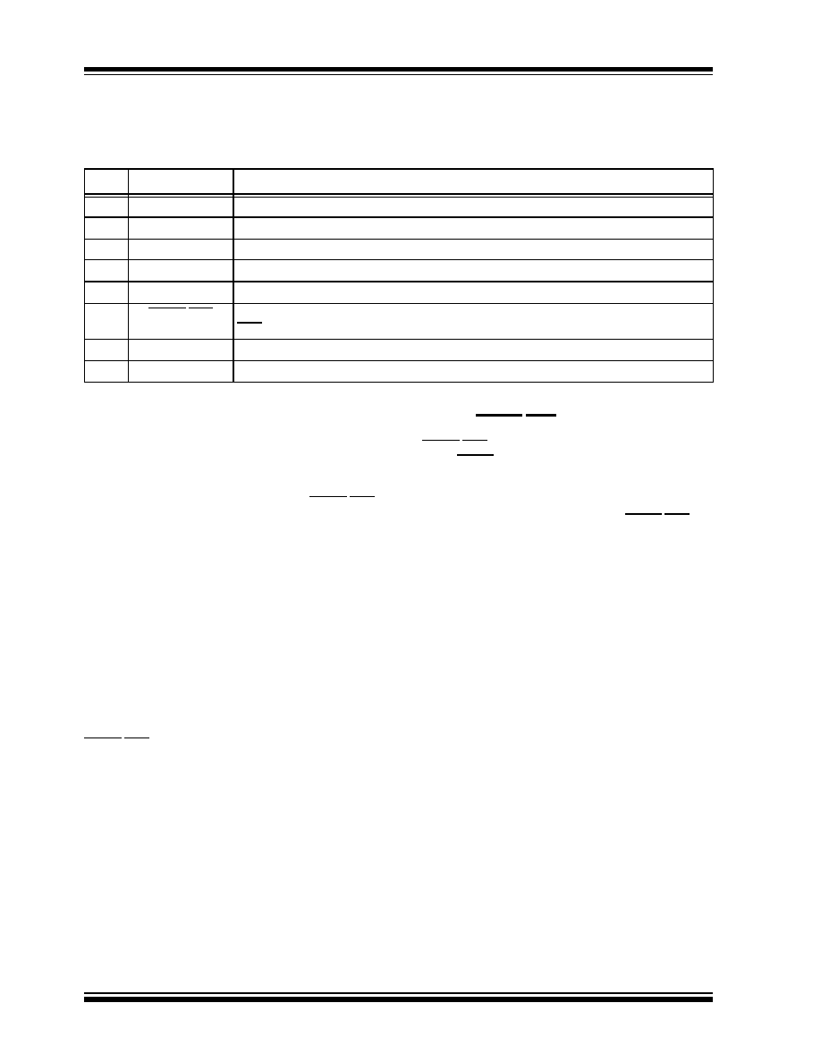
2003 Microchip Technology Inc.
DS21755B-page 9
TC646B/TC648B/TC649B
Note: Unless otherwise indicated, V
DD
= 5V, T
A
= 25°C.
FIGURE 2-13:
PWM Sink Current (I
OL
) vs.
Temperature.
FIGURE 2-14:
V
SHDN
Threshold vs.
Temperature.
FIGURE 2-15:
V
REL
Threshold vs.
Temperature.
FIGURE 2-16:
V
OTF
Threshold vs.
Temperature.
FIGURE 2-17:
Over-Temperature
Hysteresis (V
OTF-HYS
) vs. Temperature.
0
5
10
15
20
25
30
-40 -25 -10
5
20
35
50
65
80
95
110 125
Temperature (ºC)
V
OUT
I
OL
(mA)
V
DD
= 5.5V
V
DD
= 5.0V
V
DD
= 4.0V
V
DD
= 3.0V
V
OL
= 0.1V
DD
0.30
0.35
0.40
0.45
0.50
0.55
0.60
0.65
0.70
0.75
0.80
-40 -25 -10
5
20
35
50
65
80
95 110 125
Temperature (ºC)
V
SHDN
(V)
V
DD
= 3.0V
V
DD
= 4.0V
V
DD
= 5.0V
V
DD
= 5.5V
0.40
0.45
0.50
0.55
0.60
0.65
0.70
0.75
0.80
0.85
0.90
0.95
1.00
-40 -25 -10
5
20
35
50
65
80
95 110 125
Temperature (ºC)
V
REL
(V)
V
DD
= 3.0V
V
DD
= 4.0V
V
DD
= 5.0V
V
DD
= 5.5V
2.595
2.600
2.605
2.610
2.615
2.620
2.625
2.630
-40 -25 -10
5
20
35
50
65
80
95 110 125
Temperature (ºC)
V
OTF
(V)
V
DD
= 3.0V
V
DD
= 5.0V
V
DD
= 5.5V
70
75
80
85
90
95
100
-40 -25 -10
5
20
35
50
65
80
95 110 125
Temperature (ºC)
V
OTF
Hysteresis (mV)
V
DD
= 5.5V
V
DD
= 3.0V
TC646B/TC648B/TC649B
DS21755B-page 10
2003 Microchip Technology Inc.
3.0
PIN FUNCTIONS
The descriptions of the pins are given in Table 3-1.
TABLE 3-1:
PIN FUNCTION TABLE
3.1
Analog Input (V
IN
)
The thermistor network (or other temperature sensor)
connects to V
IN
. A voltage range of 1.20V to 2.60V (typ-
ical) on this pin drives an active duty cycle of 0% to
100% on the V
OUT
pin. The TC646B, TC648B and
TC649B devices enter shutdown mode when
0
V
IN
V
SHDN
. During shutdown, the FAULT/OTF
output is inactive and supply current falls to 30 µA
(typical).
3.2
Analog Output (C
F
)
C
F
is the positive terminal for the PWM ramp generator
timing capacitor. The recommended value for the C
F
capacitor is 1.0 µF for 30 Hz PWM operation.
3.3
Analog Input (V
AS
)
An external resistor divider connected to V
AS
sets the
auto-shutdown threshold. Auto-shutdown occurs when
V
IN
< V
AS
. The fan is automatically restarted when
V
IN
> (V
AS
+ V
HAS
). During auto-shutdown, the
FAULT/OTF output is inactive and supply current falls
to 30 µA (typical).
3.4
Analog Input (SENSE)
Pulses are detected at SENSE as fan rotation chops
the current through a sense resistor. The absence of
pulses indicates a fan fault condition.
3.5
Digital (Open-Drain) Output
(FAULT/OTF)
FAULT/OTF goes low to indicate a fault condition.
When FAULT goes low due to a fan fault (TC646B and
TC649B devices), the output will remain low until the
fan fault condition has been removed (16 pulses have
been detected at the SENSE pin in a 32/f period). For
the TC646B and TC648B devices, the FAULT/OTF out-
put will also be asserted when the V
IN
voltage reaches
the V
OTF
threshold of 2.62V (typical). This gives an
over-temperature/100% fan speed indication
.
3.6
Digital Output (V
OUT
)
V
OUT
is an active-high complimentary output that
drives the base of an external NPN transistor (via an
appropriate base resistor) or the gate of an N-channel
MOSFET. This output has asymmetrical drive. During a
fan fault condition, the V
OUT
output is continuously on.
3.7
Power Supply Input (V
DD
)
The V
DD
pin with respect to GND provides power to the
device. This bias supply voltage may be independent of
the fan power supply.
3.8
Ground (GND)
Ground terminal.
3.9
No Connect (NC)
No internal connection.
Pin
Name
Function
1
V
IN
Analog Input
2
C
F
Analog Output
3
V
AS
Analog Input
4
GND
Ground
5
SENSE/NC
Analog Input/No Connect. NC for TC648B.
6
FAULT/OTF
Digital (Open-Drain) Output
OTF for TC648B
7
V
OUT
Digital Output
8
V
DD
Power Supply Input
2003 Microchip Technology Inc.
DS21755B-page 11
TC646B/TC648B/TC649B
4.0
DEVICE OPERATION
The TC646B/TC648B/TC649B devices are a family of
temperature-proportional, PWM mode, fan speed con-
trollers. Features of the family include minimum fan
speed, fan auto-shutdown, fan auto-restart, remote
shutdown, over-temperature indication and fan fault
detection.
The TC64XB family is slightly different from the original
TC64X family, which includes the TC642, TC646,
TC647, TC648 and TC649 devices. Changes have
been made to adjust the operation of the device during
a fan fault condition.
The key change to the TC64XB family of devices
(TC642B, TC647B, TC646B, TC648B, TC649B) is that
the FAULT and V
OUT
outputs no longer "latch" to a
state during a fan fault condition. The TC646B/
TC648B/TC649B family will continue to monitor the
operation of the fan so that when the fan returns to nor-
mal operation, the fan speed controller will also return
to normal operation (PWM mode). The operation and
features of these devices are discussed in the following
sections.
4.1
Fan Speed Control Methods
The speed of a DC brushless fan is proportional to the
voltage across it. This relationship will vary from fan-to-
fan and should be characterized on an individual basis.
The speed versus applied voltage relationship can then
be used to set up the fan speed control algorithm.
There are two main methods for fan speed control. The
first is pulse width modulation (PWM) and the second
is linear. Using either method, the total system power
requirement to run the fan is equal. The difference
between the two methods is where the power is
consumed.
The following example compares the two methods for
a 12V, 120 mA fan running at 50% speed. With 6V
applied across the fan, the fan draws an average
current of 68 mA.
Using a linear control method, there is 6V across the
fan and 6V across the drive element. With 6V and
68 mA, the drive element is dissipating 410 mW of
power.
Using the PWM approach, the fan voltage is modulated
at a 50% duty cycle, with most of the 12V being
dropped across the fan. With 50% duty cycle, the fan
draws a RMS current of 110 mA and an average cur-
rent of 72 mA. Using a MOSFET with a 1
R
DS(on)
(a
fairly typical value for this low current), the power dissi-
pation in the drive element would be: 12 mW (Irms
2
*
R
DS(on)
). Using a standard 2N2222A NPN transistor
(assuming a Vce-sat of 0.8V), the power dissipation
would be 58 mW (Iavg* Vce-sat).
The PWM approach to fan speed control results in
much less power dissipation in the drive element. This
allows smaller devices to be used and will not require
special heatsinking to remove the power being
dissipated in the package.
The other advantage of the PWM approach is that the
voltage being applied to the fan is always near 12V.
This eliminates any concern about not supplying a high
enough voltage to run the internal fan components,
which is very relevant in linear fan speed control.
4.2
PWM Fan Speed Control
The TC646B, TC648B and TC649B devices implement
PWM fan speed control by varying the duty cycle of a
fixed-frequency pulse train. The duty cycle of a wave-
form is the on time divided by the total period of the
pulse. For example, if we take a 100 Hz waveform
(10 ms) with an on time of 5.0 ms, the duty cycle of this
waveform is 50% (5.0 ms / 10.0 ms). This example is
shown in Figure 4-1.
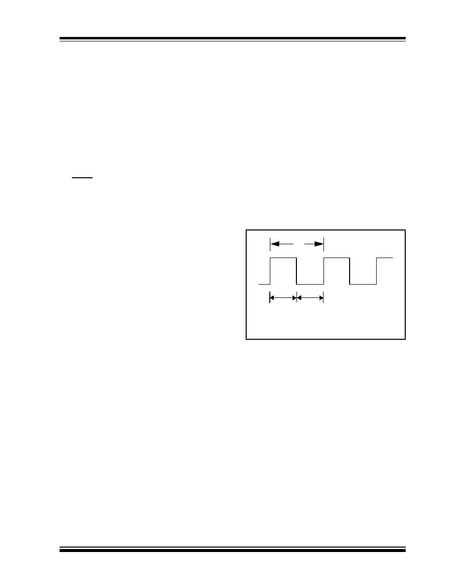
FIGURE 4-1:
Duty Cycle of a PWM
Waveform.
The TC646B/TC648B/TC649B devices generate a
pulse train with a typical frequency of 30 Hz
(C
F
= 1 µF). The duty cycle can be varied from 0% to
100%. The pulse train generated by the TC646B/
TC648B/TC649B device drives the gate of an external
N-channel MOSFET or the base of an NPN transistor.
(shown in Figure 4-2). See Section 5.5, "Output Drive
Device Selection", for more information on output drive
device selection.
t
ton
toff
t = Period
t = 1/f
f = Frequency
D = Duty Cycle
D = ton / t
TC646B/TC648B/TC649B
DS21755B-page 12
2003 Microchip Technology Inc.
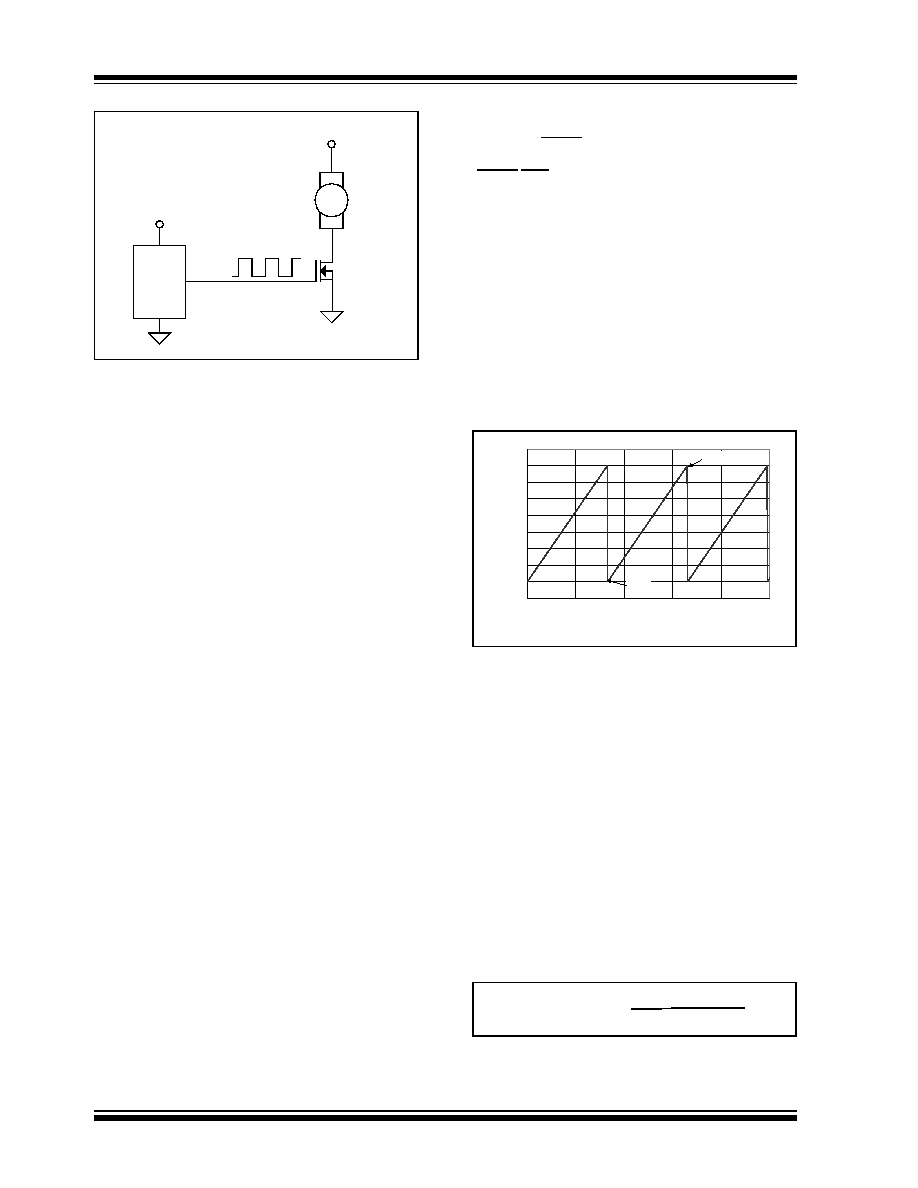
FIGURE 4-2:
PWM Fan Drive.
By modulating the voltage applied to the gate of the
MOSFET (Q
DRIVE
), the voltage that is applied to the
fan is also modulated. When the V
OUT
pulse is high, the
gate of the MOSFET is turned on, pulling the voltage at
the drain of Q
DRIVE
to zero volts. This places the full
12V across the fan for the t
on
period of the pulse. When
the duty cycle of the drive pulse is 100% (full on,
t
on
= t), the fan will run at full speed. As the duty cycle
is decreased (pulse on time "t
on
" is lowered), the fan
will slow down proportionally. With the TC646B,
TC648B and TC649B devices, the duty cycle is con-
trolled by the V
IN
input and can also be terminated by
the V
AS
input (auto-shutdown). This is described in
more detail in Section 5.5, "Output Drive Device
Selection".
4.3
Fan Start-up
Often overlooked in fan speed control is the actual
start-up control period. When starting a fan from a non-
operating condition (fan speed is zero revolutions per
minute (RPM)), the desired PWM duty cycle or average
fan voltage cannot be applied immediately. Since the
fan is at a rest position, the fan's inertia must be over-
come to get it started. The best way to accomplish this
is to apply the full rated voltage to the fan for a minimum
of one second. This will ensure that in all operating
environments, the fan will start and operate properly.
An example of the start-up timing is shown in
Figure 1-1.
A key feature of the TC646B/TC648B/TC649B devices
is the start-up timer. When power is first applied to the
device, or when the device is brought out of the shut-
down/auto-shutdown modes of operation, the V
OUT
output will go to a high state for 32 PWM cycles (one
second for C
F
= 1 µF). This will drive the fan to full
speed for this time frame.
During the start-up period for the TC646B and TC649B
devices, the SENSE pin is being monitored for fan
pulses. If pulses are detected during this period, the fan
speed controller will then move to PWM operation. If
pulses are not detected during the start-up period, the
start-up timer is activated again. If pulses are not
detected at the SENSE pin during this additional
period, the FAULT output will go low to indicate that a
fan fault condition has occurred. See Section 4.7,
"FAULT/OTF Output", for more details.
4.4
PWM Frequency & Duty Cycle
Control (C
F
& V
IN
Pins)
The frequency of the PWM pulse train is controlled by
the C
F
pin. By attaching a capacitor to the C
F
pin, the
frequency of the PWM pulse train can be set to the
desired value. The typical PWM frequency for a 1.0 µF
capacitor is 30 Hz. The frequency can be adjusted by
raising or lowering the value of the capacitor. The C
F
pin functions as a ramp generator. The voltage at this
pin will ramp from 1.20V to 2.60V (typically) as a saw-
tooth waveform. An example of this is shown in
Figure 4-3.
FIGURE 4-3:
C
F
Pin Voltage.
The duty cycle of the PWM output is controlled by the
voltage at the V
IN
input pin. The duty cycle of the PWM
output is produced by comparing the voltage at the V
IN
pin to the voltage ramp at the C
F
pin. When the voltage
at the V
IN
pin is 1.20V, the duty cycle will be 0%. When
the voltage at the V
IN
pin is 2.60V, the PWM duty cycle
will be 100% (these are both typical values). The
V
IN
-to-PWM duty cycle relationship is shown in
Figure 4-4.
The lower value of 1.20V is referred to as "V
CMIN
" and
the 2.60V threshold is referred to as "V
CMAX
". A calcu-
lation for duty cycle is shown in the equation below. The
voltage range between V
CMIN
and V
CMAX
is character-
ized as "V
CSPAN
" and has a typical value of 1.4V, with
minimum and maximum values of 1.3V and 1.5V,
respectively.
EQUATION
PWM DUTY CYCLE
FAN
12V
Q
DRIVE
TC646B
TC648B
TC649B
V
DD
GND
V
OUT
G
D
S
1.0
1.2
1.4
1.6
1.8
2.0
2.2
2.4
2.6
2.8
0
20
40
60
80
100
Time (msec)
C
F
Voltage (V)
C
F
= 1 µF
V
CMAX
V
CMIN
Duty Cycle (%) =
V
CMAX
- V
CMIN
(V
IN
- V
CMIN
) * 100
2003 Microchip Technology Inc.
DS21755B-page 13
TC646B/TC648B/TC649B
For the TC646B, TC648B and TC649B devices, the V
IN
pin is also used as the shutdown pin. The V
SHDN
and
V
REL
threshold voltages are characterized in the "Elec-
trical Characteristics Table" of Section 1.0. If the V
IN
pin
voltage is pulled below the V
SHDN
threshold, the device
will shut down (V
OUT
output goes to a low state, the
FAULT/OTF pin is inactive). If the voltage on the V
IN
pin
then rises above the release threshold (V
REL
), the
device will go through a power-up sequence (assuming
that the V
IN
voltage is also higher than the voltage at
the V
AS
pin). The power-up sequence is shown later in
the "Behavioral Algorithm Flowcharts" of Section 4.9.
FIGURE 4-4:
V
IN
Voltage vs. PWM Duty
Cycle (Typical).
4.5
Auto-Shutdown Mode (V
AS
)
For the TC646B, TC648B and TC649B devices, pin 3
is the V
AS
pin and is used for setting the auto-shutdown
threshold voltage.
The auto-shutdown function provides a way to set a
threshold voltage (temperature) at which the fan will be
shut off. This way, if the temperature in the system
reaches a threshold at which the fan(s) no longer needs
to operate, the fan can be shutdown automatically.
The voltage range for the V
AS
pin is the same as the
voltage range for the V
IN
pin (1.20V to 2.60V). The volt-
age at the V
AS
pin is set in this range so that when the
voltage at the V
IN
pin decreases below the voltage at
the V
AS
pin (signifying that the threshold temperature
has been reached), the V
OUT
output is shut off (goes to
a low state). In auto-shutdown, the FAULT/OTF output
is inactive (high-impedance). Auto-shutdown mode is
exited when the V
IN
voltage exceeds the V
AS
voltage
by the auto-shutdown hysteresis voltage (V
HAS
). Upon
exiting auto-shutdown mode, the start-up timer is
triggered and the device returns to normal operation.
4.6
V
OUT
Output (PWM Output)
The V
OUT
output is a digital output designed for driving
the base of a transistor or the gate of a MOSFET. The
V
OUT
output is designed to be able to quickly raise the
base current or the gate voltage of the external drive
device to its final value.
When the device is in shutdown/auto-shutdown mode,
the V
OUT
output is actively held low. The output can be
varied from 0% (full off) to 100% duty cycle (full on). As
previously discussed, the duty cycle of the V
OUT
output
is controlled via the V
IN
input voltage and can be termi-
nated based on the V
AS
voltage.
A base current-limiting resistor is required when using
a transistor as the external drive device in order to limit
the amount of drive current that is drawn from the V
OUT
output.
The V
OUT
output can be directly connected to the gate
of an external MOSFET. One concern when doing this,
though, is that the fast turn-off time of the fan drive
MOSFET can cause a problem because the fan motor
looks like an inductor. When the MOSFET is turned off
quickly, the current in the fan wants to continue to flow
in the same direction. This causes the voltage at the
drain of the MOSFET to rise. If there aren't any clamp
diodes internal to the fan, this voltage can rise above
the drain-to-source voltage rating of the MOSFET. For
this reason, an external clamp diode is suggested. This
is shown in Figure 4-5.
FIGURE 4-5:
Clamp Diode for Fan.
4.7
FAULT/OTF Output
The FAULT/OTF output is an open-drain, active-low
output. For the TC646B and TC649B devices, pin 6 is
labeled as the FAULT output and indicates when a fan
fault condition has occurred. For the TC646B device,
the FAULT output also indicates when an over-temper-
ature (OTF) condition has occurred. For the TC648B
device, pin 6 is the OTF output that indicates an over-
temperature (OTF) condition has occurred.
0
10
20
30
40
50
60
70
80
90
100
1
1.2
1.4
1.6
1.8
2
2.2
2.4
2.6
2.8
V
IN
(V)
Duty Cycle (%)
Q
1
GND
R
SENSE
V
OUT
Q
1
: N-Channel MOSFET
FAN
Clamp Diode
TC646B/TC648B/TC649B
DS21755B-page 14
2003 Microchip Technology Inc.
For the TC646B and TC648B devices, an over-temper-
ature condition is indicated when the V
IN
input reaches
the V
OTF
threshold voltage (the V
OTF
threshold voltage
is typically 20 mV higher than the V
CMAX
threshold and
has 80 mV of hysteresis). This indicates that maximum
cooling capacity has been reached (the fan is at full
speed) and that an overheating situation can occur.
When the voltage at the V
IN
input falls below the V
OTF
threshold voltage by the hysteresis value (V
OTF-HYS
),
the FAULT/OTF output will return to the high state (a
pull-up resistor is needed on the FAULT/OTF output).
For the TC646B/TC649B devices, a fan fault condition
is indicated when fan current pulses are no longer
detected at the SENSE pin. Pulses at the SENSE pin
indicate that the fan is spinning and conducting current.
If pulses are not detected at the SENSE pin for
32 PWM cycles, the 3-cycle diagnostic timer is fired.
This means that the V
OUT
output is high for 3 PWM
cycles. If pulses are detected in this 3-cycle period, nor-
mal PWM operation is resumed and no fan fault is indi-
cated. If no pulses are detected in the 3-cycle period,
the start-up timer is activated and the V
OUT
output is
driven high for 32 PWM cycles. If pulses are detected
during this time-frame, normal PWM operation is
resumed. If no pulses are detected during this time-
period, a fan fault condition exists and the FAULT
output is pulled low.
During a fan fault condition, the FAULT output will
remain low until the fault condition has been removed.
During this time, the V
OUT
output is driven high contin-
uously to attempt to restart the fan and the SENSE pin
is monitored for fan pulses. If a minimum of 16 pulses
are detected at the SENSE input over a 32 cycle time-
period (one second for C
F
= 1.0 µF), the fan fault con-
dition no longer exists. Therefore, The FAULT output is
released and the V
OUT
output returns to normal PWM
operation, as dictated by the V
IN
and V
AS
inputs.
If the V
IN
voltage is pulled below the V
SHDN
level during
a fan fault condition, the FAULT output will be released
and the V
OUT
output will be shutdown (V
OUT
= 0V). If
the V
IN
voltage then increases above the V
REL
thresh-
old and is above the V
AS
voltage, the device will go
through the normal start-up routine.
If, during a fan fault condition, the voltage at the V
IN
pin
drops below the V
AS
voltage level, the TC646B/
TC649B device will continue to hold the FAULT line low
and drive the V
OUT
output to 100% duty cycle. If the fan
fault condition is then removed, the FAULT output will
be released and the TC646B/TC649B device will enter
auto-shutdown mode until the V
IN
voltage is brought
above the V
AS
voltage by the auto-shutdown hysteresis
value (V
HAS
). The TC646B/TC649B device will then
resume normal PWM mode operation.
The sink current capability of the FAULT output is listed
in the "Electrical Characteristics Table" of Section 1.0.
4.8
Sensing Fan Operation (SENSE)
The SENSE input is an analog input used to monitor
the fan's operation (the TC648B device does not incor-
porate the fan sensing feature). It does this by sensing
fan current pulses that represent fan rotation. When a
fan rotates, commutation of the fan current occurs as
the fan poles pass the armatures of the motor. The
commutation of the fan current makes the current
waveshape appear as pulses. There are two typical
current waveforms of brushless DC fan motors,
illustrated in Figures 4-6 and 4-7.
FIGURE 4-6:
Fan Current With DC Offset
And Positive Commutation Current.
FIGURE 4-7:
Fan Current With
Commutation Pulses To Zero.
2003 Microchip Technology Inc.
DS21755B-page 15
TC646B/TC648B/TC649B
The SENSE pin senses positive voltage pulses that
have an amplitude of 70 mV (typical value). Each time
a pulse is detected, the missing pulse detector timer
(t
MP
) is reset. As previously stated, if the missing pulse
detector timer reaches the time for 32 cycles, the loop
for diagnosing a fan fault is engaged (diagnostic timer,
then the start-up timer).
Both of the fan current waveshapes shown in Figures
4-6 and 4-7 can be sensed with the sensing scheme
shown in Figure 4-8.
FIGURE 4-8:
Sensing Scheme For Fan
Current.
The fan current flowing through R
SENSE
generates a
voltage that is proportional to the current. The C
SENSE
capacitor removes any DC portion of the voltage
across R
SENSE
and presents only the voltage pulse
portion to the SENSE pin of the TC646B/TC649B
devices.
The R
SENSE
and C
SENSE
values need to be selected so
that the voltage pulse provided to the SENSE pin is
70 mV (typical) in amplitude. Be sure to check the
sense pulse amplitude over all operating conditions
(duty cycles) as the current pulse amplitude will vary
with duty cycle. See Section 5.0, "Applications Informa-
tion", for more details on selecting values for R
SENSE
and C
SENSE
.
Key features of the SENSE pin circuitry are an initial
blanking period after every V
OUT
pulse and an initial
pulse blanker.
The TC646B/TC649B sense circuitry has a blanking
period that occurs at the turn-on of each V
OUT
pulse.
During this blanking period, the sense circuitry ignores
any pulse information that is seen at the SENSE pin
input. This stops the TC646B/TC649B device from
falsely sensing a current pulse that is due to the fan
drive device turn-on.
The initial pulse blanker is also implemented to stop
false sensing of fan current pulses. When a fan is in a
locked rotor condition, the fan current no longer com-
mutates, it simply flows through one fan winding and is
a DC current. When a fan is in a locked rotor condition
and the TC646B/TC649B device is in PWM mode, it
will see one current pulse each time the V
OUT
output is
turned on. The initial pulse blanker allows the
TC646B/TC649B device to ignore this pulse and
recognize that the fan is in a fault condition.
4.9
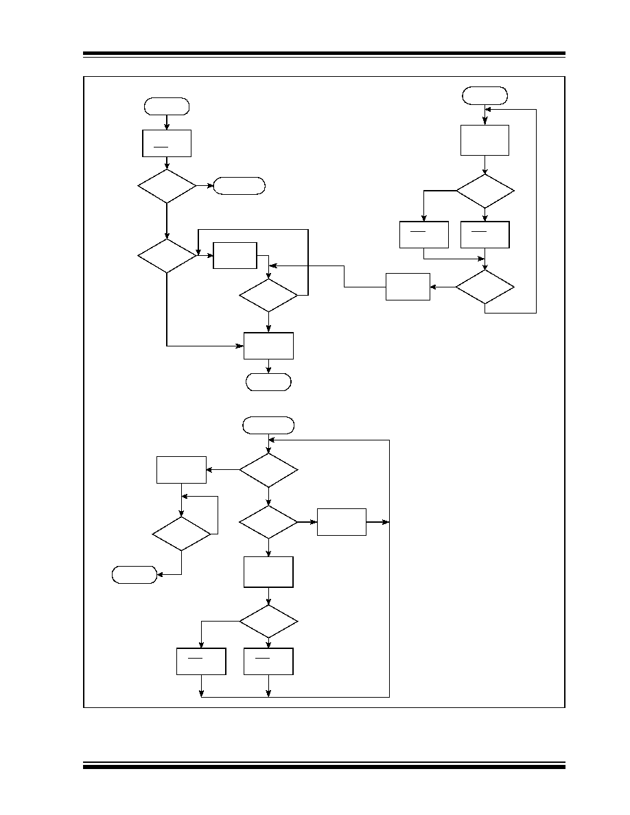
Behavioral Algorithms
The behavioral algorithms for the TC646B/TC649B
and TC648B devices are shown in Figure 4-9 and
Figure 4-10, respectively.
The behavioral algorithms show the step-by-step deci-
sion-making process for the fan speed controller oper-
ation. The TC646B and TC649B devices are very
similar with one exception: the TC649B device does
not implement the over-temperature portion of the
algorithm.
R
ISO
R
SENSE
C
SENSE
(0.1 µF typical)
SENSE
V
OUT
TC64XB
GND
FAN
TC646B/TC648B/TC649B
DS21755B-page 16
2003 Microchip Technology Inc.
FIGURE 4-9:
TC646B/TC649B Behavioral Algorithm.
Fire Start-up
Timer
(1 sec)
Fan Pulse
Detected?
Fan Pulse
Detected?
V
IN
< V
SHDN
?
V
IN
< V
AS
?
Shutdown
V
OUT
= 0
Auto-
Shutdown
V
OUT
= 0
Yes
No
No
No
No
Yes
Yes
Yes
Power-Up
Normal
Operation
Fan Fault
Power-on
Reset
FAULT = 1
V
IN
> V
REL
?
No
V
IN
>
(V
AS
+ V
HAS
)
Yes
Yes
No
Hot Start
Fire Start-up
Timer
(1 sec)
Fire Start-up
Timer
(1 sec)
V
IN
> V
REL?
Yes
Fan Fault
Clear Missing
Pulse Detector
V
OUT
Proportional
to V
IN
V
IN
< V
SHDN
?
V
IN
< V
AS
?
V
IN
> V
OTF
?
M.P.D.
Expired?
Fan Pulse
Detected?
Shutdown
V
OUT
= 0
Auto
Shutdown
V
OUT
= 0
No
No
No
No
No
No
Yes
Yes
Yes
Yes
Normal
Operation
Power-Up
V
IN
>
(V
AS
+ V
HAS
)
No
Yes
Hot Start
Yes
No
FAULT = 0
Yes
Fire
Diagnostic
Timer
(100 msec)
Fan Pulse
Detected?
Fan Pulse
Detected?
Yes
No
FAULT = Low,
V
OUT
= High
16 Pulses
Detected?
No
Yes
Power-Up
V
IN
< V
SHDN
?
V
IN
> V
REL
?
Fan Fault
Yes
Normal
Operation
Shutdown
V
OUT
= 0
Yes
No
No
TC646B Only
2003 Microchip Technology Inc.
DS21755B-page 17
TC646B/TC648B/TC649B
FIGURE 4-10:
TC648B Behavioral Algorithm.
V
AS
= 0V
V
IN
< V
AS
?
Auto-
Shutdown
V
OUT
= 0
Yes
No
No
Yes
Power-Up
Power-on
Reset
OTF = 1
V
IN
>
(V
AS
+ V
HAS
)
Yes
No
Fire Start-up
Timer
(1 sec)
V
IN
> 1.20V
V
OUT
Proportional
to V
IN
V
IN
> V
OTF
?
Auto
Shutdown
V
OUT
= 0
No
No
Yes
Normal
Operation
V
OUT
= 0
No
Yes
Yes
Minimum
Speed Mode
Normal
Operation
OTF = 1
OTF = 0
V
IN
< V
AS
?
Minimum
Speed Mode
V
IN
= 0V
Power-Up
V
IN
> 1.20V
V
OUT
Proportional
to V
IN
V
IN
> V
OTF
?
No
Yes
OTF = 1
OTF = 0
V
OUT
= 0
Yes
No
No
Yes
TC646B/TC648B/TC649B
DS21755B-page 18
2003 Microchip Technology Inc.
5.0
APPLICATIONS INFORMATION
5.1
Setting the PWM Frequency
The PWM frequency of the V
OUT
output is set by the
capacitor value attached to the C
F
pin. The PWM fre-
quency will be 30 Hz (typical) for a 1 µF capacitor. The
relationship between frequency and capacitor value is
linear, making alternate frequency selections easy.
As stated in previous sections, the PWM frequency
should be kept in the range of 15 Hz to 35 Hz. This will
eliminate the possibility of having audible frequencies
when varying the duty cycle of the fan drive.
A very important factor to consider when selecting the
PWM frequency for the TC646B/TC648B/TC649B
devices is the RPM rating of the selected fan and the
minimum duty cycle that you will be operating at. For
fans that have a full-speed rating of 3000 RPM or less,
it is desirable to use a lower PWM frequency. A lower
PWM frequency allows for a longer time-period to mon-
itor the fan current pulses. The goal is to be able to
monitor at least two fan current pulses during the on-
time of the V
OUT
output.
Example: The system design requirement is to operate
the fan at 50% duty cycle when ambient temperatures
are below 20°C. The fan full-speed RPM rating is
3000 RPM and has four current pulses per rotation. At
50% duty cycle, the fan will be operating at
approximately 1500 RPM.
EQUATION
If one fan revolution occurs in 40 msec, each fan pulse
occurs 10 msec apart. In order to detect two fan current
pulses, the on-time of the V
OUT
pulse must be at least
20 msec. With the duty cycle at 50%, the total period of
one cycle must be at least 40 msec, which makes the
PWM frequency 25 Hz. For this example, a PWM fre-
quency of 20 Hz is recommended. This would define a
C
F
capacitor value of 1.5 µF.
5.2
Temperature Sensor Design
As discussed in previous sections, the V
IN
analog input
has a range of 1.20V to 2.60V (typical), which repre-
sents a duty cycle range on the V
OUT
output of 0% to
100%, respectively. The V
IN
voltages can be thought of
as representing temperatures. The 1.20V level is the
low temperature at which the system requires very little
cooling. The 2.60V level is the high temperature, for
which the system needs maximum cooling capability
(100% fan speed).
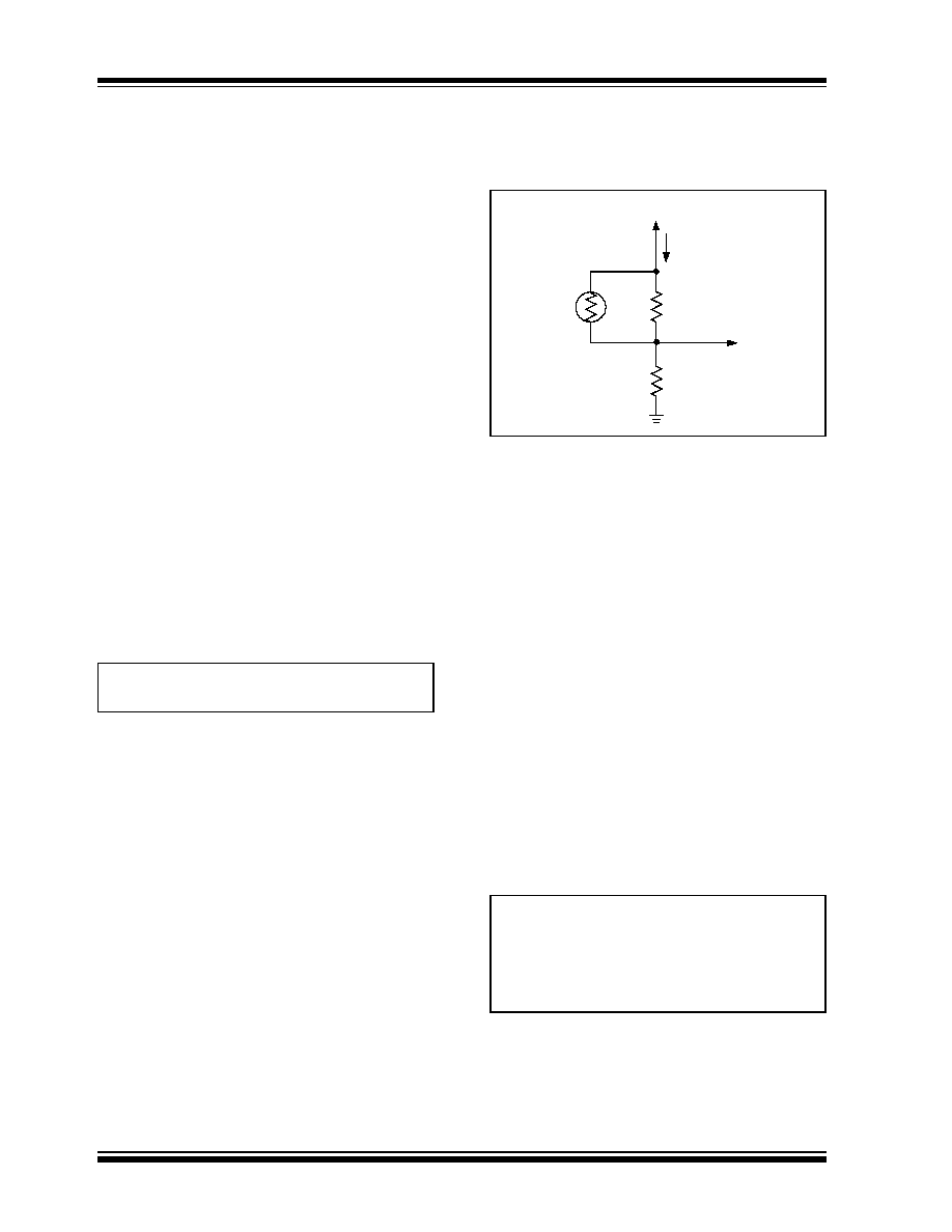
One of the simplest ways of sensing temperature over
a given range is to use a thermistor. By using a NTC
thermistor, as shown in Figure 5-1, a temperature-
variant voltage can be created.
FIGURE 5-1:
Temperature Sensing
Circuit.
Figure 5-1 represents a temperature-dependent, volt-
age divider circuit. R
T
is a conventional NTC thermistor,
R
1
and R
2
are standard resistors. R
1
and R
T
form a
parallel resistor combination that will be referred to as
R
TEMP
(R
TEMP
= R
1
* R
T
/ R
1
+ R
T
). As the temperature
increases, the value of R
T
decreases and the value of
R
TEMP
will decrease with it. Accordingly, the voltage at
V
IN
increases as temperature increases, giving the
desired relationship for the V
IN
input. R
1
helps to linear-
ize the response of the SENSE network and aids in
obtaining the proper V
IN
voltages over the desired tem-
perature range. An example of this is shown in
Figure 5-2.
If less current draw from V
DD
is desired, a larger value
thermistor should be chosen. The voltage at the V
IN
pin
can also be generated by a voltage output temperature
sensor device. The key is to get the desired V
IN
volt-
age-to-system (or component) temperature relation-
ship.
The following equations apply to the circuit in
Figure 5-1.
EQUATION
In order to solve for the values of R
1
, R
2
, V
IN
and the
temperatures at which they are to occur, need to be
selected. The variables T1 and T2 represent the
selected temperatures. The value of the thermistor at
these two temperatures can be found in the thermistor
Time for one revolution (msec.)
60 1000
×
1500
------------------------
40
=
=
R
2
R
1
R
T
I
DIV
V
IN
V
DD
V T1
( )
VDD R2
×
RTEMP T1
( ) R2
+
----------------------------------------------
=
V T2
( )
VDD R2
×
RTEMP T2
( ) R2
+
----------------------------------------------
=
2003 Microchip Technology Inc.
DS21755B-page 19
TC646B/TC648B/TC649B
data sheet. With the values for the thermistor and the
values for V
IN
, you now have two equations from which
the values for R
1
and R
2
can be found.
Example: The following design goals are desired:
· Duty Cycle = 50% (V
IN
= 1.90V) with Temperature
(T1) = 30°C
· Duty Cycle = 100% (V
IN
= 2.60V) with
Temperature (T2) = 60°C
Using a 100 k
thermistor (25°C value), we look up the
thermistor values at the desired temperatures:
· R
T
(T1) = 79428
@ 30°C
· R
T
(T2) = 22593
@ 60°C
Substituting these numbers into the given equations
produces the following numbers for R
1
and R
2
.
· R
1
= 34.8 k
· R
2
= 14.7 k
FIGURE 5-2:
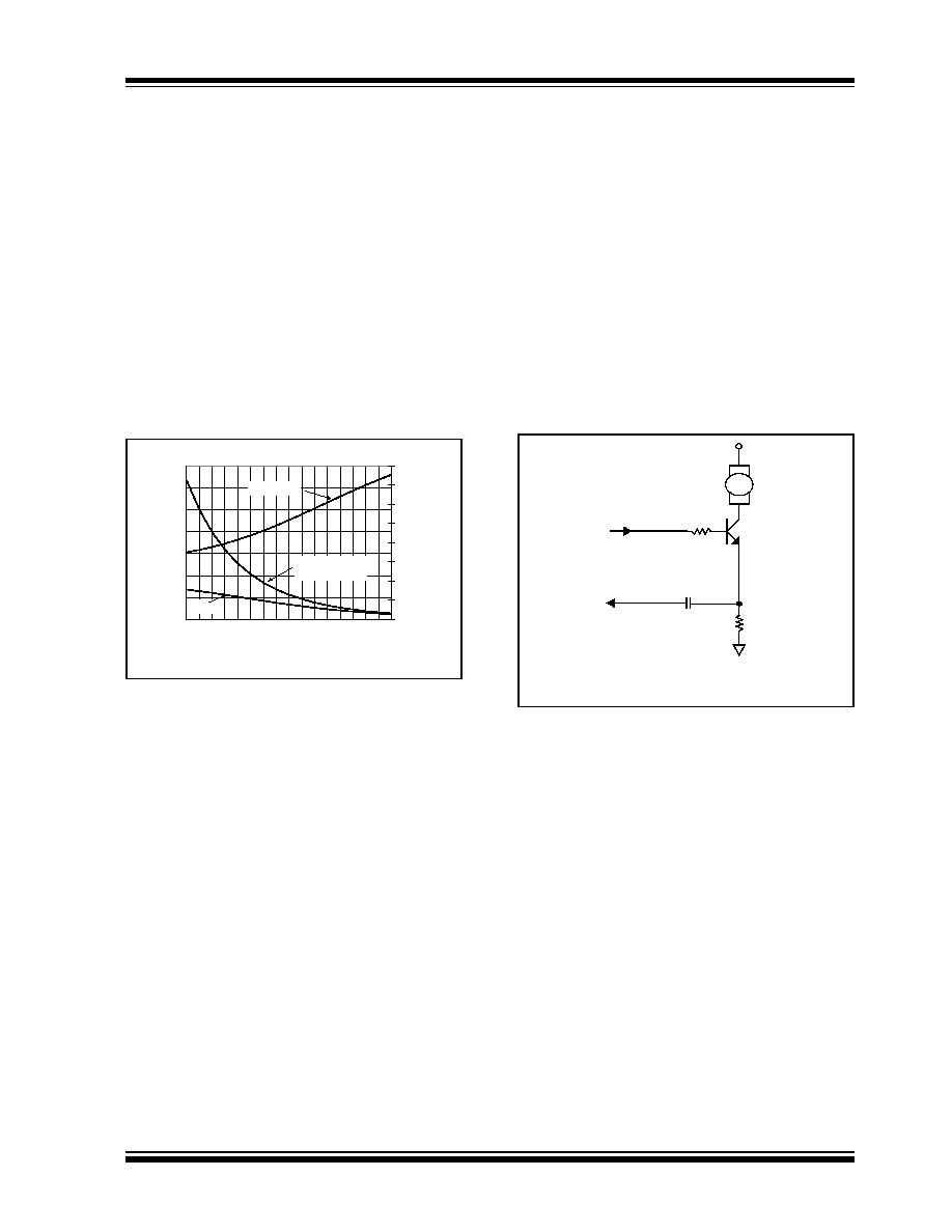
How Thermistor Resistance,
V
IN
, and R
TEMP
Vary With Temperature.
Figure 5-2 graphs R
T
, R
TEMP
(R
1
in parallel with R
T
)
and V
IN
, versus temperature for the example shown
above.
5.3
Thermistor Selection
As with any component, there are a number of sources
for thermistors. A listing of companies that manufacture
thermistors can be found at www.temperatures.com/
thermivendors.html. This website lists over forty
suppliers of thermistor products. A brief list is shown
here:
5.4
FanSense Network
(R
SENSE
and C
SENSE
)
The SENSE network (comprised of R
SENSE
and
C
SENSE
) allows the TC646B and TC649B devices to
detect commutation of the fan motor. R
SENSE
converts
the fan current into a voltage. C
SENSE
AC couples this
voltage signal to the SENSE pin. The goal of the
SENSE network is to provide a voltage pulse to the
SENSE pin that has a minimum amplitude of 90 mV.
This will ensure that the current pulse caused by the
fan commutation is recognized by the TC646B/
TC649B device.
A 0.1 µF ceramic capacitor is recommended for
C
SENSE
. Smaller values will require that larger sense
resistors be used. Using a 0.1 µF capacitor results in
reasonable values for R
SENSE
. Figure 5-3 illustrates a
typical SENSE network.
FIGURE 5-3:
Typical Sense Network.
The required value of R
SENSE
will change with the cur-
rent rating of the fan and the fan current waveshape. A
key point is that the current rating of the fan specified
by the manufacturer may be a worst-case rating, with
the actual current drawn by the fan being lower than
this rating. For the purposes of setting the value for
R
SENSE
, the operating fan current should be measured
to get the nominal value. This can be done by using an
oscilloscope current probe or using a voltage probe
with a low-value resistor (0.5
). Another good tool for
this exercise is the TC642 Evaluation Board. This
board allows the R
SENSE
and C
SENSE
values to be eas-
ily changed while allowing the voltage waveforms to be
monitored to ensure the proper levels are being
reached.
Table 5-1 shows values of R
SENSE
according to the
nominal operating current of the fan. The fan currents
are average values. If the fan current falls between two
of the values listed, use the higher resistor value.
-
Thermometrics
®
-
Quality Thermistor
TM
-
Ametherm
®
-
Sensor Scientific
TM
-
U.S. Sensor
TM
-
Vishay
®
-
Advanced Thermal
Products
TM
-
muRata
®
0
20
40
60
80
100
120
140
20
30
40
50
60
70
80
90
100
Temperature (ºC)
Network Resistance (k
)
0.000
0.500
1.000
1.500
2.000
2.500
3.000
3.500
4.000
V
IN
(V)
NTC Thermistor
100 k @ 25ºC
V
IN
Voltage
R
TEMP
FAN
R
ISO
R
SENSE
C
SENSE
SENSE
V
OUT
(0.1 µF typical)
715
Note:
See Table 5-1 for R
SENSE
values.
TC646B/TC648B/TC649B
DS21755B-page 20
2003 Microchip Technology Inc.
TABLE 5-1:
FAN CURRENT VS. R
SENSE
The values listed in Table 5-1 are for fans that have the
fan current waveshape shown in Figure 4-7. With this
waveshape, the average fan current is closer to the
peak value, which requires the resistor value to be
higher. When using a fan that has the fan current wave-
shape shown in Figure 4-6, the resistor value can often
be decreased since the current peaks are higher than
the average and it is the AC portion of the voltage that
gets coupled to the SENSE pin.
The key point when selecting an R
SENSE
value is to try
to minimize the value in order to minimize the power
dissipation in the resistor. In order to do this, it is critical
to know the waveshape of the fan current and not just
the average value.
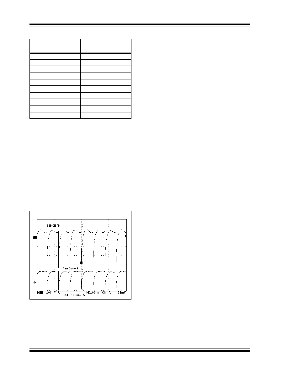
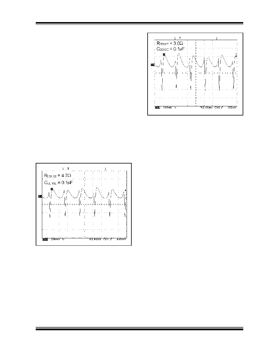
Figure 5-4 shows some typical waveforms for the fan
current and the voltage at the SENSE pin.
FIGURE 5-4:
Typical Fan Current and
SENSE Pin Waveforms.
Another important factor to consider when selecting the
R
SENSE
value is the fan current value during a locked-
rotor condition. When a fan is in a locked-rotor condi-
tion (fan blades are stopped even though power is
being applied to the fan), the fan current can increase
dramatically (often 2.5 to 3.0 times the normal operat-
ing fan current). This will effect the power rating of the
R
SENSE
resistor selected.
When selecting the fan for the application, the current
draw of the fan during a locked-rotor condition should
be considered. Especially if multiple fans are being
used in the application.
There are two main types of fan designs when looking
at fan current draw during a locked-rotor condition.
The first is a fan that will simply draw high DC currents
when put into a locked-rotor condition. Many older fans
were designed this way. An example of this is a fan that
draws an average current of 100 mA during normal
operation. In a locked-rotor condition, this fan will draw
250 mA of average current. For this design, the
R
SENSE
power rating must be sized to handle the
250 mA condition. The fan bias supply must also take
this into account.
The second style design, which represents many of the
newer fan designs today, acts to limit the current in a
locked-rotor condition by going into a pulse mode of
operation. An example of the fan current waveshape
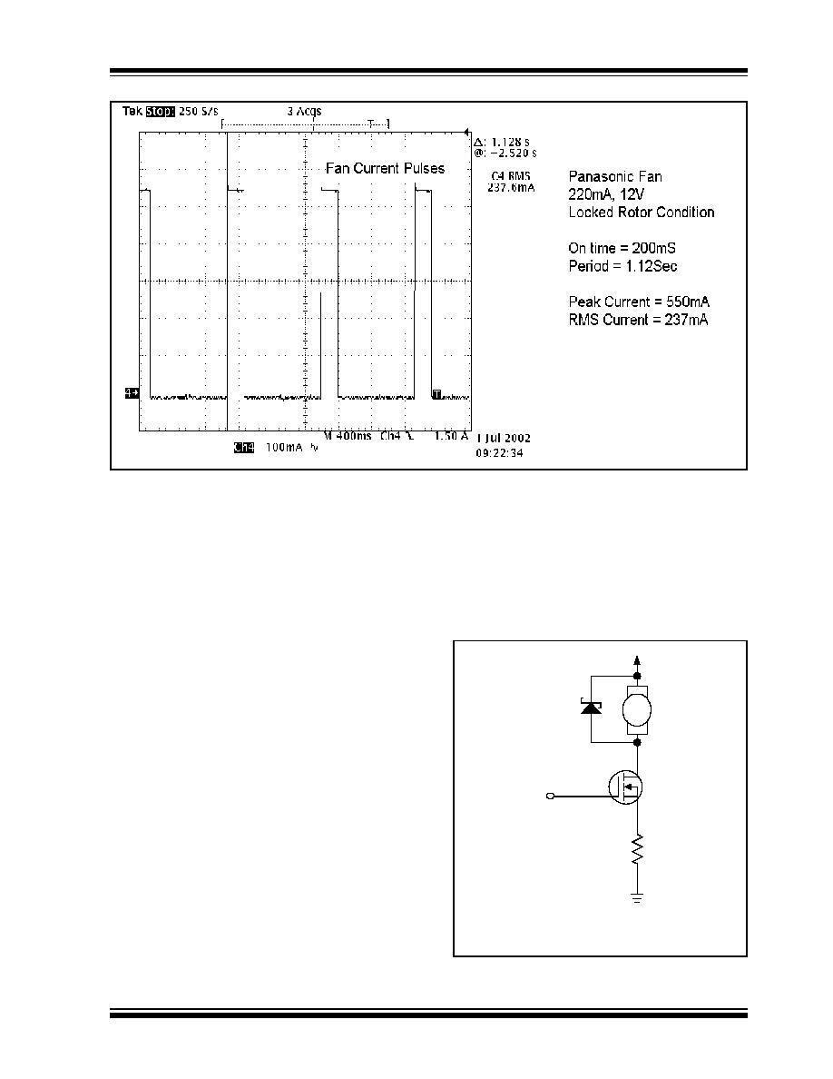
for this style fan is shown in Figure 5-5. The fan repre-
sented in Figure 5-5 is a Panasonic
®
, 12V, 220 mA fan.
During the on-time of the waveform, the fan current is
peaking up to 550 mA. Due to the pulse mode opera-
tion, the actual RMS current of the fan is very near the
220 mA rating. Because of this, the power rating for the
R
SENSE
resistor does not have to be oversized for this
application.
Nominal Fan Current
(mA)
R
SENSE
(
)
50
9.1
100
4.7
150
3.0
200
2.4
250
2.0
300
1.8
350
1.5
400
1.3
450
1.2
500
1.0
2003 Microchip Technology Inc.
DS21755B-page 21
TC646B/TC648B/TC649B
FIGURE 5-5:
Fan Current During a Locked Rotor Condition.
5.5
Output Drive Device Selection
The TC646B/TC648B/TC649B is designed to drive an
external NPN transistor or N-channel MOSFET as the
fan speed modulating element. These two arrange-
ments are shown in Figure 5-7. For lower-current fans,
NPN transistors are a very economical choice for the
fan drive device. It is recommended that, for higher cur-
rent fans (300 mA and above), MOSFETs be used as
the fan drive device. Table 5-2 provides some possible
part numbers for use as the fan drive element.
When using a NPN transistor as the fan drive element,
a base current-limiting resistor must be used. This is
shown in Figure 5-7.
When using MOSFETs as the fan drive element, it is
very easy to turn the MOSFETs on and off at very high
rates. Because the gate capacitances of these small
MOSFETs are very low, the TC646B/TC648B/TC649B
can charge and discharge them very quickly, leading to
very fast edges. Of key concern is the turn-off edge of
the MOSFET. Since the fan motor winding is essentially
an inductor, once the MOSFET is turned off the current
that was flowing through the motor wants to continue to
flow. If the fan does not have internal clamp diodes
around the windings of the motor, there is no path for
this current to flow through and the voltage at the drain
of the MOSFET may rise until the drain-to-source rating
of the MOSFET is exceeded. This will most likely cause
the MOSFET to go into avalanche mode. Since there is
very little energy in this occurrence, it will probably not
fail the device, but it would be a long-term reliability
issue.
The following is recommended:
· Ask how the fan is designed. If the fan has clamp
diodes internally, this problem will not be seen. If
the fan does not have internal clamp diodes, it is a
good idea to install one externally (Figure 5-6).
Putting a resistor between V
OUT
and the gate of
the MOSFET will also help slow down the turn-off
and limit this condition.
FIGURE 5-6:
Clamp Diode For Fan Turn-
Off.
Q
1
GND
R
SENSE
V
OUT
Q
1
: N-Channel MOSFET
FAN
TC646B/TC648B/TC649B
DS21755B-page 22
2003 Microchip Technology Inc.
FIGURE 5-7:
Output Drive Device Configurations.
TABLE 5-2:
FAN DRIVE DEVICE SELECTION TABLE (NOTE 2)
5.6
Bias Supply Bypassing and Noise
Filtering
The bias supply (V
DD
) for the TC646B/TC648B/
TC649B devices should be bypassed with a 1.0 µF
ceramic capacitor. This capacitor will help supply the
peak currents that are required to drive the base/gate
of the external fan drive devices.
As the V
IN
pin controls the duty cycle in a linear fashion,
any noise on this pin can cause duty cycle jittering. For
this reason, the V
IN
pin should be bypassed with a
0.01 µF capacitor.
In order to keep fan noise off of the TC646B/TC648B/
TC649B device ground, individual ground returns for
the TC646B/TC648B/TC649B and the low side of the
fan current sense resistor should be used.
5.7
Design Example/Typical
Application
The system has been designed with the following
components and criteria:
System inlet air ambient temperature ranges from 0ºC
to 50ºC. At 20ºC, system cooling is no longer required,
so the fan is to be turned off. Prior to turn-off, the fan
should be run at 40% of its full fan speed. Full fan
speed should be reached when the ambient air is 40ºC.
The system has a surface mount, NTC-style thermistor
in a 1206 package. The thermistor is mounted on a
daughtercard that is directly in the inlet air stream. The
thermistor is a NTC, 100 k
@ 25ºC, Thermometrics
®
part number NHQ104B425R5. The given Beta for the
thermistor is 4250. The system bias voltage to run the
fan controller is 5V, while the fan voltage is 12V.
Device
Package
Max Vbe sat /
Vgs(V)
Min hfe
V
CE
/V
DS
(V)
Fan Current
(mA)
Suggested
Rbase (
)
MMBT2222A
SOT-23
1.2
50
40
150
800
MPS2222A
TO-92
1.2
50
40
150
800
MPS6602
TO-92
1.2
50
40
500
301
SI2302
SOT-23
2.5
NA
20
500
Note 1
MGSF1N02E
SOT-23
2.5
NA
20
500
Note 1
SI4410
SO-8
4.5
NA
30
1000
Note 1
SI2308
SOT-23
4.5
NA
60
500
Note 1
Note 1:
A series gate resistor may be used in order to control the MOSFET turn-on and turn-off times.
2:
These drive devices are suggestions only. Fan currents listed are for individual fans.
Q
1
GND
Fan Bias
R
SENSE
R
BASE
V
OUT
FAN
a) Single Bipolar Transistor
Q
1
GND
Fan Bias
R
SENSE
V
OUT
b) N-Channel MOSFET
FAN
2003 Microchip Technology Inc.
DS21755B-page 23
TC646B/TC648B/TC649B
The fan used in the system is a Panasonic
®
, Panaflo
®
-
series fan, model number FBA06T12H.
A fault indication is desired when the fan is in a locked-
rotor condition. This signal is used to indicate to the
system that cooling is not available and a warning
should be issued to the user. No fault indication from
the fan controller is necessary for an over-temperature
condition as this is being reported elsewhere.
Step 1: Gathering Information.
The first step in the design process is to gather the
needed data on the fan and thermistor. For the fan, it is
also a good idea to look at the fan current waveform, as
indicated earlier in the data sheet.
Fan Information: Panasonic number: FBA06T12H
- Voltage = 12V
- Current = 145 mA (data sheet number)
FIGURE 5-8:
FBA06T12H Fan Current
Waveform.
From the waveform in Figure 5-8, the fan current has
an average value of 120 mA, with peaks up to 150 mA.
This information will help in the selection of the R
SENSE
and C
SENSE
values later on. Also of interest for the
R
SENSE
selection value is what the fan current does in
a locked-rotor condition.
FIGURE 5-9:
FBA06T12H Locked-Rotor
Fan Current.
From Figure 5-9, it is seen that in a locked-rotor fault
condition, the fan goes into a pulsed current mode of
operation. During this mode, when the fan is conduct-
ing current, the peak current value is 360 mA for peri-
ods of 200 msec. This is significantly higher than the
average full fan speed current shown in Figure 5-8.
However, because of the pulse mode, the average fan
current in a locked-rotor condition is lower and was
measured at 68 mA. The RMS current during this
mode, which is necessary for current sense resistor
(R
SENSE
) value selection, was measured at 154 mA.
This is slightly higher than the RMS value during full fan
speed operation.
Thermistor Information: Thermometrics part number:
NHQ104B425R5
- Resistance Value: 100 k
@ 25ºC
- Beta Value (
): 4250
From this information, the thermistor values at 20ºC
and 40ºC must be found. This information is needed in
order to select the proper resistor values for R
1
and R
2
(see Figure 5-13), which sets the V
IN
voltage.
The equation for determining the thermistor values is
shown below:
EQUATION
R
T0
is the thermistor value at 25ºC. T
0
is 298.15 and T
is the temperature of interest. All temperatures are in
degrees kelvin.
Using this equation, the values for the thermistor are
found to be:
- R
T
(20ºC) = 127,462
- R
T
(40ºC) = 50,520
R
T
R
TO
T
O
T
(
)
T T
O
·
------------------------
exp
=
TC646B/TC648B/TC649B
DS21755B-page 24
2003 Microchip Technology Inc.
Step 2: Selecting the Fan Controller.
The requirements for the fan controller are that it have
auto-shutdown capability at 20ºC and also indicate a
fan fault condition. No over-temperature indication is
necessary. From these specifications, the proper
selection is the TC649B device.
Step 3: Setting the PWM Frequency.
The fan is rated at 4200 RPM with a 12V input. The
goal is to run to a 40% duty cycle (roughly 40% fan
speed), which equates to approximately 1700 RPM. At
1700 RPM, one full fan revolution occurs every
35 msec. The fan being used is a four-pole fan that
gives four current pulses per revolution. With this infor-
mation, and viewing test results at 40% duty cycle, two
fan current pulses were always seen during the PWM
on time with a PWM frequency of 30 Hz. For this rea-
son, the C
F
value is selected to be 1.0 µF.
Step 4: Setting the V
IN
Voltage.
From the design criteria, the desired duty cycle at 20ºC
is 40% and full fan speed should be reached at 40ºC.
Based on a V
IN
voltage range of 1.20V to 2.60V, which
represents 0% to 100% duty cycle, the 40% duty cycle
voltage can be found using the following equation:
EQUATION
Using the above equation, the V
IN
values are
calculated to be:
- V
IN
(40%) = 1.76V
- V
IN
(100%) = 2.60V
Using these values along with the thermistor resistance
values calculated earlier, the R
1
and R
2
resistor values
can now be calculated using the following equation:
EQUATION
R
TEMP
is the parallel combination of R
1
and the ther-
mistor. V(T1) represents the V
IN
voltage at 20ºC and
V(T2) represents the V
IN
voltage at 40ºC. Solving the
equations simultaneously yields the following values
(V
DD
= 5V):
- R
1
= 238,455
- R
2
= 45,161
Using standard 1% resistor values, the selected R
1
and
R
2
values are:
- R
1
= 237 k
- R
2
= 45.3 k
A graph of the V
IN
voltage, thermistor resistance and
R
TEMP
resistance versus temperature for this
configuration is shown in Figure 5-10.
FIGURE 5-10:
Thermistor Resistance, V
IN
and R
TEMP
vs. Temperature
Step 5: Setting the Auto-Shutdown Voltage (V
AS
).
Setting the voltage for the auto-shutdown is done using
a simple resistor voltage divider. The criteria for the
voltage divider in this design is that it draw no more
than 100 µA of current. The required auto-shutdown
voltage was determined earlier in the selection of the
V
IN
voltage at 40% duty cycle, since this was also set
at the temperature that auto-shutdown is to occur
(20ºC).
- V
AS
= 1.76V
Given this desired setpoint and knowing the desired
divider current, the following equations can be used to
solve for the resistor values for R
3
and R
4
:
EQUATION
Using the equations above, the resistor values for R
3
and R
4
are found to be:
- R
3
= 32.4 k
- R
4
= 17.6 k
Using standard 1% resistor values yields the following
values:
- R
3
= 32.4 k
- R
4
= 17.8 k
V
IN
= (DC * 1.4V) + 1.20V
DC = Desired Duty Cycle
V T1
( )
V
DD
R
2
×
R
TEMP
T1
( ) R
2
+
------------------------------------------
=
V T2
( )
V
DD
R
2
×
R
TEMP
T2
( ) R
2
+
------------------------------------------
=
0
50
100
150
200
250
300
350
400
0
10
20
30
40
50
60
70
80
90
Temperature (ºC)
Network Resistance (k
)
0.00
0.50
1.00
1.50
2.00
2.50
3.00
3.50
4.00
4.50
5.00
V
IN
(V)
V
IN
NTC Thermistor
100 k @ 25ºC
R
TEMP
I
DIV
=
5V
R
3
+ R
4
V
AS
=
5V * R
4
R
3
+ R
4
2003 Microchip Technology Inc.
DS21755B-page 25
TC646B/TC648B/TC649B
Step 6: Selecting the Fan Drive Device (Q
1
).
Since the fan operating current is below 200 mA, a
transistor or MOSFET can be used as the fan drive
device. In order to reduce component count and cur-
rent draw, the drive device for this design is chosen to
be a N-channel MOSFET. Selecting from Table 5-2,
there are two MOSFETs that are good choices, the
MGSF1N02E and the SI2302. These devices have the
same pinout and are interchangeable for this design.
Step 7: Selecting the R
SENSE
and C
SENSE
Values.
The goal again for selecting these values is to ensure
that the signal at the SENSE pin is 90 mV in amplitude
under all operating conditions. This will ensure that the
pulses are detected by the TC649B device and that the
fan operation is detected.
The fan current waveform is shown in Figure 5-8, and
as discussed previously, with a waveform of this shape,
the current sense resistor values shown in Table 5-1 are
good reference values. Given the average fan operating
current was measured to be 120 mA, this falls between
two of the values listed in the table. For reference pur-
poses, both values have been tested and these results
are shown in Figures 5-11 (4.7
) and 5-12 (3.0). The
selected C
SENSE
value is 0.1 µF, as this provides the
appropriate coupling of the voltage to the SENSE pin.
FIGURE 5-11:
SENSE pin voltage with
4.7
sense resistor.
FIGURE 5-12:
SENSE pin voltage with
3.0
sense resistor.
Since the 3.0
value of sense resistor provides the
proper voltage to the SENSE pin, it is the correct choice
for this solution as it will also provide the lowest power
dissipation and the maximum amount of voltage to the
fan. Using the RMS fan current which was measured
previously, the power dissipation in the resistor during
a fan fault condition is 71 mW (Irms
2
* R
SENSE
). This
number will set the wattage rating of the resistor that is
selected. The selected value will vary depending upon
the derating guidelines that are used.
Now that all the values have been selected, the sche-
matic representation of this design can be seen in
Figure 5-13.
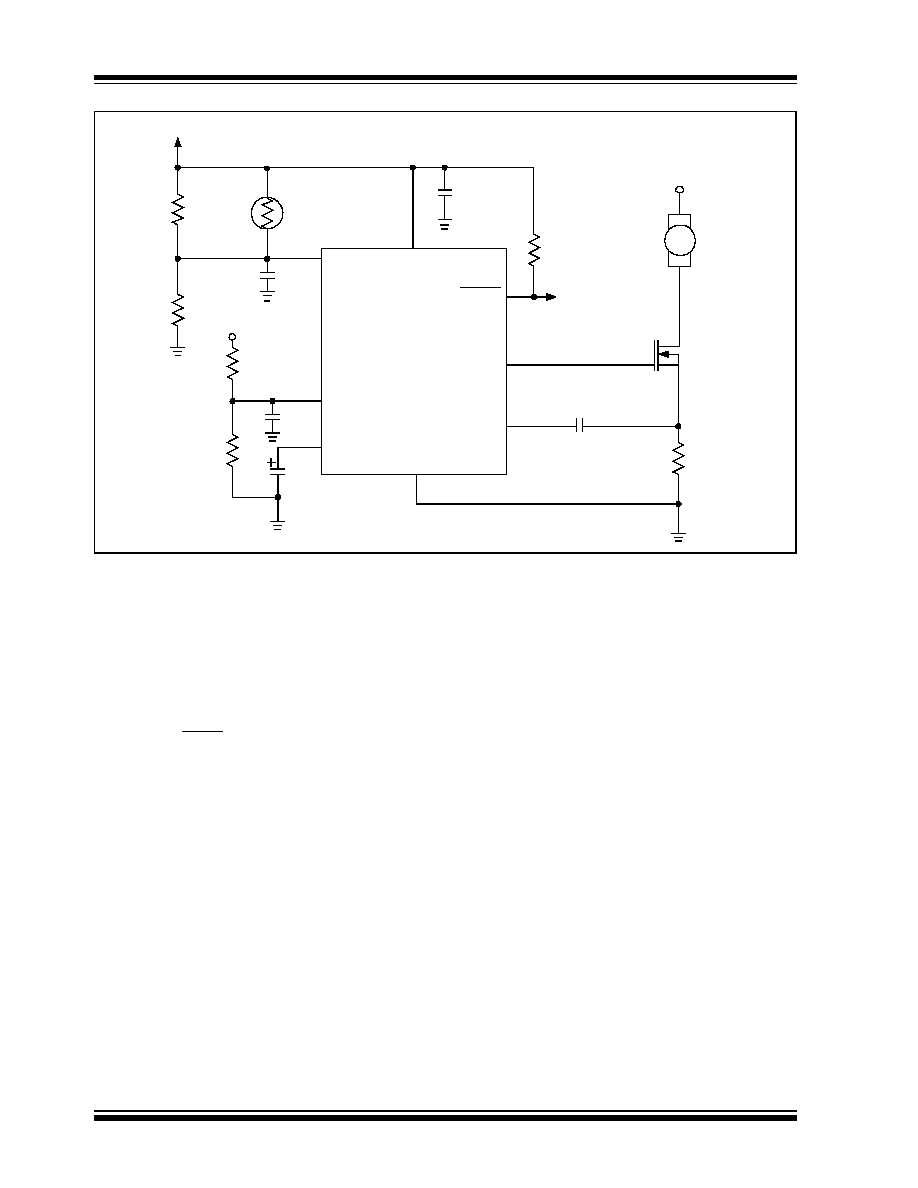
TC646B/TC648B/TC649B
DS21755B-page 26
2003 Microchip Technology Inc.
FIGURE 5-13:
Design Example Schematic.
Bypass capacitor C
VDD
is added to the design to
decouple the bias voltage. This is good to have, espe-
cially when using a MOSFET as the drive device. This
helps to give a localized low-impedance source for the
current required to charge the gate capacitance of Q
1
.
Two other bypass capacitors (labeled as C
B
) were also
added to decouple the V
IN
and V
AS
nodes. These were
added simply to remove any noise present that might
cause false triggerings or PWM jitter. R
5
is the pull-up
resistor for the FAULT output. The value for this resistor
is system-dependent.
FAULT
SENSE
R
1
R
2
R
3
32.4 k
R
4
GND
Q
1
+12V
+5V
V
DD
V
IN
V
AS
V
OUT
R
SENSE
C
SENSE
C
F
1.0 µF
C
F
TC649B
Fan
C
B
0.01 µF
C
B
0.01 µF
+
4
5
7
6
8
1
3
2
+5V
17.8 k
237 k
45.3k
R
5
10 k
0.1 µF
SI2302
or
MGSF1N02E
Panasonic
®
12V, 140 mA
FBA06T12H
Thermometrics
®
100 k
@25°C
NHQ104B425R5
1.0 µF
3.0
C
VDD
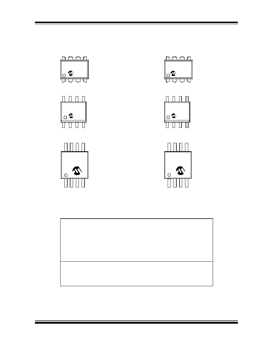
2003 Microchip Technology Inc.
DS21755B-page 27
TC646B/TC648B/TC649B
6.0
PACKAGING INFORMATION
6.1
Package Marking Information
XXXXXXXXX
NNN
YYWW
8-Lead PDIP (300 mil)
Example
:
8-Lead SOIC (150 mil)
Example
:
XXXXXX
XXXYYWW
NNN
TC646BCPA
025
0215
TC646B
COA0215
025
8-Lead MSOP
Example
:
XXXXXX
YWWNNN
TC646B
215025
Legend: XX...X
Customer specific information*
Y
Year code (last digit of calendar year)
YY
Year code (last 2 digits of calendar year)
WW
Week code (week of January 1 is week `01')
NNN
Alphanumeric traceability code
Note:
In the event the full Microchip part number cannot be marked on one line, it will
be carried over to the next line thus limiting the number of available characters
for customer specific information.
*
Standard device marking consists of Microchip part number, year code, week code, and traceability
code.
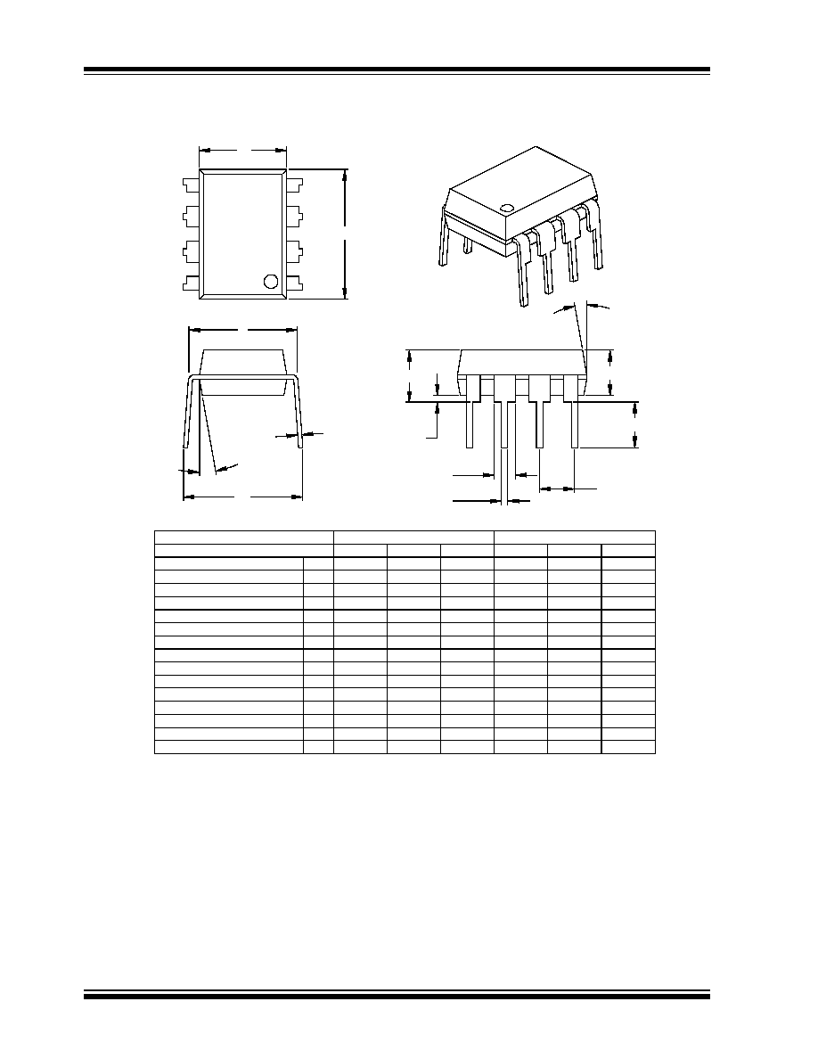
TC646B/TC648B/TC649B
DS21755B-page 28
2003 Microchip Technology Inc.
8-Lead Plastic Dual In-line (PA) 300 mil (PDIP)
B1
B
A1
A
L
A2
p
E
eB
c
E1
n
D
1
2
Units
INCHES*
MILLIMETERS
Dimension Limits
MIN
NOM
MAX
MIN
NOM
MAX
Number of Pins
n
8
8
Pitch
p
.100
2.54
Top to Seating Plane
A
.140
.155
.170
3.56
3.94
4.32
Molded Package Thickness
A2
.115
.130
.145
2.92
3.30
3.68
Base to Seating Plane
A1
.015
0.38
Shoulder to Shoulder Width
E
.300
.313
.325
7.62
7.94
8.26
Molded Package Width
E1
.240
.250
.260
6.10
6.35
6.60
Overall Length
D
.360
.373
.385
9.14
9.46
9.78
Tip to Seating Plane
L
.125
.130
.135
3.18
3.30
3.43
Lead Thickness
c
.008
.012
.015
0.20
0.29
0.38
Upper Lead Width
B1
.045
.058
.070
1.14
1.46
1.78
Lower Lead Width
B
.014
.018
.022
0.36
0.46
0.56
Overall Row Spacing
§
eB
.310
.370
.430
7.87
9.40
10.92
Mold Draft Angle Top
5
10
15
5
10
15
Mold Draft Angle Bottom
5
10
15
5
10
15
* Controlling Parameter
Notes:
Dimensions D and E1 do not include mold flash or protrusions. Mold flash or protrusions shall not exceed
JEDEC Equivalent: MS-001
Drawing No. C04-018
.010" (0.254mm) per side.
§ Significant Characteristic
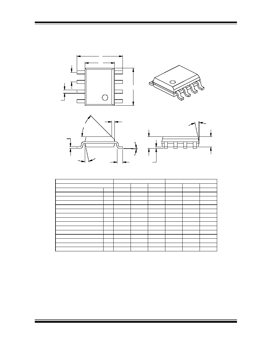
2003 Microchip Technology Inc.
DS21755B-page 29
TC646B/TC648B/TC649B
8-Lead Plastic Small Outline (OA) Narrow, 150 mil (SOIC)
Foot Angle
f
0
4
8
0
4
8
15
12
0
15
12
0
Mold Draft Angle Bottom
15
12
0
15
12
0
Mold Draft Angle Top
0.51
0.42
0.33
.020
.017
.013
B
Lead Width
0.25
0.23
0.20
.010
.009
.008
c
Lead Thickness
0.76
0.62
0.48
.030
.025
.019
L
Foot Length
0.51
0.38
0.25
.020
.015
.010
h
Chamfer Distance
5.00
4.90
4.80
.197
.193
.189
D
Overall Length
3.99
3.91
3.71
.157
.154
.146
E1
Molded Package Width
6.20
6.02
5.79
.244
.237
.228
E
Overall Width
0.25
0.18
0.10
.010
.007
.004
A1
Standoff §
1.55
1.42
1.32
.061
.056
.052
A2
Molded Package Thickness
1.75
1.55
1.35
.069
.061
.053
A
Overall Height
1.27
.050
p
Pitch
8
8
n
Number of Pins
MAX
NOM
MIN
MAX
NOM
MIN
Dimension Limits
MILLIMETERS
INCHES*
Units
2
1
D
n
p
B
E
E1
h
L
c
45×
f
A2
A
A1
* Controlling Parameter
Notes:
Dimensions D and E1 do not include mold flash or protrusions. Mold flash or protrusions shall not exceed
.010" (0.254mm) per side.
JEDEC Equivalent: MS-012
Drawing No. C04-057
§ Significant Characteristic
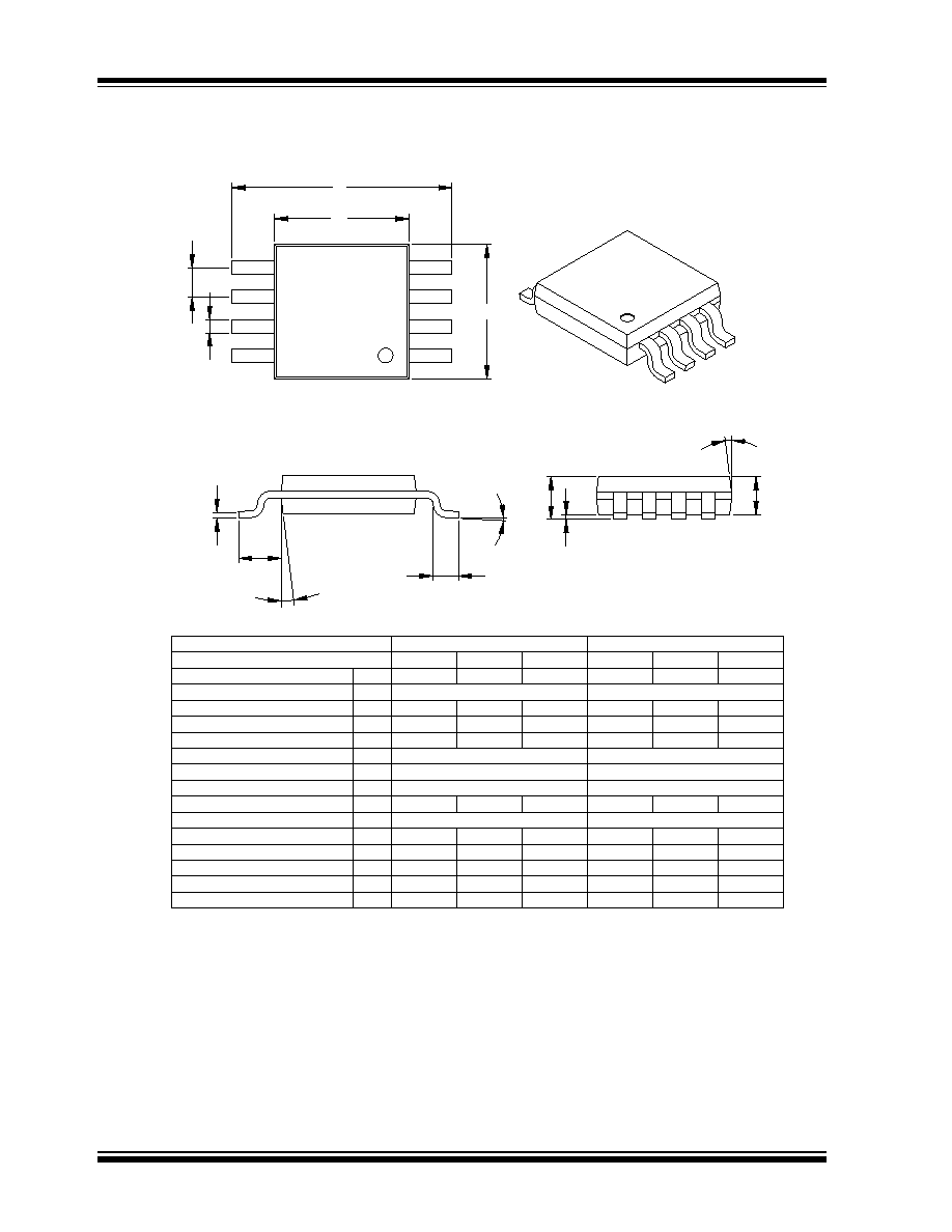
TC646B/TC648B/TC649B
DS21755B-page 30
2003 Microchip Technology Inc.
8-Lead Plastic Micro Small Outline Package (UA) (MSOP)
D
A
A1
L
c
(F)
A2
E1
E
p
B
n
1
2
Dimensions D and E1 do not include mold flash or protrusions. Mold flash or protrusions shall not
.037 REF
F
Footprint (Reference)
exceed .010" (0.254mm) per side.
Notes:
Drawing No. C04-111
*Controlling Parameter
Mold Draft Angle Top
Mold Draft Angle Bottom
Foot Angle
Lead Width
Lead Thickness
c
B
.003
.009
.006
.012
Dimension Limits
Overall Height
Molded Package Thickness
Molded Package Width
Overall Length
Foot Length
Standoff
Overall Width
Number of Pins
Pitch
A
L
E1
D
A1
E
A2
.016
.024
.118 BSC
.118 BSC
.000
.030
.193 TYP.
.033
MIN
p
n
Units
.026 BSC
NOM
8
INCHES
0.95 REF
-
-
.009
.016
0.08
0.22
0°
0.23
0.40
8°
MILLIMETERS*
0.65 BSC
0.85
3.00 BSC
3.00 BSC
0.60
4.90 BSC
.043
.031
.037
.006
0.40
0.00
0.75
MIN
MAX
NOM
1.10
0.80
0.15
0.95
MAX
8
-
-
-
15°
5°
-
15°
5°
-
JEDEC Equivalent: MO-187
0°
-
8°
5°
5°
-
-
15°
15°
-
-
-
-
2003 Microchip Technology Inc.
DS21755B-page 31
TC646B/TC648B/TC649B
6.2
Taping Form
PIN 1
Component Taping Orientation for 8-Pin MSOP Devices
User Direction of Feed
Standard Reel Component Orientation
for 713 or TR Suffix Device
W
P
Carrier Tape, Number of Components Per Reel and Reel Size:
Package
Carrier Width (W)
Pitch (P)
Part Per Full Reel
Reel Size
8-Pin MSOP
12 mm
8 mm
2500
13 in.
PIN 1
Component Taping Orientation for 8-Pin SOIC Devices
User Direction of Feed
Standard Reel Component Orientation
for 713 or TR Suffix Device
W
P
Carrier Tape, Number of Components Per Reel and Reel Size:
Package
Carrier Width (W)
Pitch (P)
Part Per Full Reel
Reel Size
8-Pin SOIC
12 mm
8 mm
2500
13 in.

TC646B/TC648B/TC649B
DS21755B-page 32
2003 Microchip Technology Inc.
NOTES:

2003 Microchip Technology Inc.
DS21755B-page 33
TC646B/TC648B/TC649B
PRODUCT IDENTIFICATION SYSTEM
To order or obtain information, e.g., on pricing or delivery, refer to the factory or the listed sales office
.
Sales and Support
Device:
TC646B: PWM Fan Speed Controller with Fan
Restart, Auto-Shutdown, Fan Fault and
Over-Temp Detection
TC648B: PWM Fan Speed Controller with Auto-
Shutdown and Over-Temp Detection
TC649B: PWM Fan Speed Controller with Fan
Restart, Auto-Shutdown and Fan Fault
Detection
Temperature
Range:
E
= -40°C to +85°C
Package:
OA = Plastic SOIC, (150 mil Body), 8-lead
PA = Plastic DIP (300 mil Body), 8-lead
UA = Plastic Micro Small Outline (MSOP), 8-lead
713 = Tape and Reel (SOIC and MSOP)
(TC646B and TC648B only)
TR = Tape and Reel (SOIC and MSOP) (TC649B
only)
PART NO.
X
/XX
Package
Temperature
Range
Device
Examples:
a)
TC646BEOA: SOIC package.
b)
TC646BEOA713: Tape and Reel,
SOIC package.
c)
TC646BEPA: PDIP package.
d)
TC646BEUA: MSOP package.
a)
TC648BEOA: SOIC package.
b)
TC648BEPA: PDIP package.
c)
TC648BEUA: MSOP package.
d)
TC648BEUA713: Tape and Reel,
MSOP package.
a)
TC649BEOA: SOIC package.
b)
TC649BEOATR: Tape and Reel,
SOIC package.
c)
TC649BEPA: PDIP package.
d)
TC649BEUA: MSOP package
Data Sheets
Products supported by a preliminary Data Sheet may have an errata sheet describing minor operational differences and
recommended workarounds. To determine if an errata sheet exists for a particular device, please contact one of the following:
1.
Your local Microchip sales office
2.
The Microchip Corporate Literature Center U.S. FAX: (480) 792-7277
3.
The Microchip Worldwide Site (www.microchip.com)
Please specify which device, revision of silicon and Data Sheet (include Literature #) you are using.
Customer Notification System
Register on our web site (www.microchip.com/cn) to receive the most current information on our products.

TC646B/TC648B/TC649B
DS21755B-page 34
2003 Microchip Technology Inc.
NOTES:

DS21755B-page 35
2003 Microchip Technology Inc.
Information contained in this publication regarding device
applications and the like is intended through suggestion only
and may be superseded by updates. It is your responsibility to
ensure that your application meets with your specifications.
No representation or warranty is given and no liability is
assumed by Microchip Technology Incorporated with respect
to the accuracy or use of such information, or infringement of
patents or other intellectual property rights arising from such
use or otherwise. Use of Microchip's products as critical
components in life support systems is not authorized except
with express written approval by Microchip. No licenses are
conveyed, implicitly or otherwise, under any intellectual
property rights.
Trademarks
The Microchip name and logo, the Microchip logo, K
EE
L
OQ
,
MPLAB, PIC, PICmicro, PICSTART, PRO MATE and
PowerSmart are registered trademarks of Microchip
Technology Incorporated in the U.S.A. and other countries.
FilterLab, microID, MXDEV, MXLAB, PICMASTER, SEEVAL
and The Embedded Control Solutions Company are
registered trademarks of Microchip Technology Incorporated
in the U.S.A.
Accuron, Application Maestro, dsPIC, dsPICDEM,
dsPICDEM.net, ECONOMONITOR, FanSense, FlexROM,
fuzzyLAB, In-Circuit Serial Programming, ICSP, ICEPIC,
microPort, Migratable Memory, MPASM, MPLIB, MPLINK,
MPSIM, PICC, PICkit, PICDEM, PICDEM.net, PowerCal,
PowerInfo, PowerMate, PowerTool, rfLAB, rfPIC, Select
Mode, SmartSensor, SmartShunt, SmartTel and Total
Endurance are trademarks of Microchip Technology
Incorporated in the U.S.A. and other countries.
Serialized Quick Turn Programming (SQTP) is a service mark
of Microchip Technology Incorporated in the U.S.A.
All other trademarks mentioned herein are property of their
respective companies.
© 2003, Microchip Technology Incorporated, Printed in the
U.S.A., All Rights Reserved.
Printed on recycled paper.
Note the following details of the code protection feature on Microchip devices:
·
Microchip products meet the specification contained in their particular Microchip Data Sheet.
·
Microchip believes that its family of products is one of the most secure families of its kind on the market today, when used in the
intended manner and under normal conditions.
·
There are dishonest and possibly illegal methods used to breach the code protection feature. All of these methods, to our
knowledge, require using the Microchip products in a manner outside the operating specifications contained in Microchip's Data
Sheets. Most likely, the person doing so is engaged in theft of intellectual property.
·
Microchip is willing to work with the customer who is concerned about the integrity of their code.
·
Neither Microchip nor any other semiconductor manufacturer can guarantee the security of their code. Code protection does not
mean that we are guaranteeing the product as "unbreakable."
Code protection is constantly evolving. We at Microchip are committed to continuously improving the code protection features of our
products. Attempts to break microchip's code protection feature may be a violation of the Digital Millennium Copyright Act. If such acts
allow unauthorized access to your software or other copyrighted work, you may have a right to sue for relief under that Act.
Microchip received QS-9000 quality system
certification for its worldwide headquarters,
design and wafer fabrication facilities in
Chandler and Tempe, Arizona in July 1999
and Mountain View, California in March 2002.
The Company's quality system processes and
procedures are QS-9000 compliant for its
PICmicro
®
8-bit MCUs, K
EE
L
OQ
®
code hopping
devices, Serial EEPROMs, microperipherals,
non-volatile memory and analog products. In
addition, Microchip's quality system for the
design and manufacture of development
systems is ISO 9001 certified.

DS21755B-page 36
2003 Microchip Technology Inc.
M
AMERICAS
Corporate Office
2355 West Chandler Blvd.
Chandler, AZ 85224-6199
Tel: 480-792-7200 Fax: 480-792-7277
Technical Support: 480-792-7627
Web Address: http://www.microchip.com
Atlanta
3780 Mansell Road, Suite 130
Alpharetta, GA 30022
Tel: 770-640-0034 Fax: 770-640-0307
Boston
2 Lan Drive, Suite 120
Westford, MA 01886
Tel: 978-692-3848 Fax: 978-692-3821
Chicago
333 Pierce Road, Suite 180
Itasca, IL 60143
Tel: 630-285-0071 Fax: 630-285-0075
Dallas
4570 Westgrove Drive, Suite 160
Addison, TX 75001
Tel: 972-818-7423 Fax: 972-818-2924
Detroit
Tri-Atria Office Building
32255 Northwestern Highway, Suite 190
Farmington Hills, MI 48334
Tel: 248-538-2250 Fax: 248-538-2260
Kokomo
2767 S. Albright Road
Kokomo, IN 46902
Tel: 765-864-8360 Fax: 765-864-8387
Los Angeles
18201 Von Karman, Suite 1090
Irvine, CA 92612
Tel: 949-263-1888 Fax: 949-263-1338
Phoenix
2355 West Chandler Blvd.
Chandler, AZ 85224-6199
Tel: 480-792-7966 Fax: 480-792-4338
San Jose
Microchip Technology Inc.
2107 North First Street, Suite 590
San Jose, CA 95131
Tel: 408-436-7950 Fax: 408-436-7955
Toronto
6285 Northam Drive, Suite 108
Mississauga, Ontario L4V 1X5, Canada
Tel: 905-673-0699 Fax: 905-673-6509
ASIA/PACIFIC
Australia
Microchip Technology Australia Pty Ltd
Marketing Support Division
Suite 22, 41 Rawson Street
Epping 2121, NSW
Australia
Tel: 61-2-9868-6733 Fax: 61-2-9868-6755
China - Beijing
Microchip Technology Consulting (Shanghai)
Co., Ltd., Beijing Liaison Office
Unit 915
Bei Hai Wan Tai Bldg.
No. 6 Chaoyangmen Beidajie
Beijing, 100027, No. China
Tel: 86-10-85282100 Fax: 86-10-85282104
China - Chengdu
Microchip Technology Consulting (Shanghai)
Co., Ltd., Chengdu Liaison Office
Rm. 2401-2402, 24th Floor,
Ming Xing Financial Tower
No. 88 TIDU Street
Chengdu 610016, China
Tel: 86-28-86766200 Fax: 86-28-86766599
China - Fuzhou
Microchip Technology Consulting (Shanghai)
Co., Ltd., Fuzhou Liaison Office
Unit 28F, World Trade Plaza
No. 71 Wusi Road
Fuzhou 350001, China
Tel: 86-591-7503506 Fax: 86-591-7503521
China - Hong Kong SAR
Microchip Technology Hongkong Ltd.
Unit 901-6, Tower 2, Metroplaza
223 Hing Fong Road
Kwai Fong, N.T., Hong Kong
Tel: 852-2401-1200 Fax: 852-2401-3431
China - Shanghai
Microchip Technology Consulting (Shanghai)
Co., Ltd.
Room 701, Bldg. B
Far East International Plaza
No. 317 Xian Xia Road
Shanghai, 200051
Tel: 86-21-6275-5700 Fax: 86-21-6275-5060
China - Shenzhen
Microchip Technology Consulting (Shanghai)
Co., Ltd., Shenzhen Liaison Office
Rm. 1812, 18/F, Building A, United Plaza
No. 5022 Binhe Road, Futian District
Shenzhen 518033, China
Tel: 86-755-82901380 Fax: 86-755-82966626
China - Qingdao
Rm. B505A, Fullhope Plaza,
No. 12 Hong Kong Central Rd.
Qingdao 266071, China
Tel: 86-532-5027355 Fax: 86-532-5027205
India
Microchip Technology Inc.
India Liaison Office
Marketing Support Division
Divyasree Chambers
1 Floor, Wing A (A3/A4)
No. 11, O'Shaugnessey Road
Bangalore, 560 025, India
Tel: 91-80-2290061 Fax: 91-80-2290062
Japan
Microchip Technology Japan K.K.
Benex S-1 6F
3-18-20, Shinyokohama
Kohoku-Ku, Yokohama-shi
Kanagawa, 222-0033, Japan
Tel: 81-45-471- 6166 Fax: 81-45-471-6122
Korea
Microchip Technology Korea
168-1, Youngbo Bldg. 3 Floor
Samsung-Dong, Kangnam-Ku
Seoul, Korea 135-882
Tel: 82-2-554-7200 Fax: 82-2-558-5934
Singapore
Microchip Technology Singapore Pte Ltd.
200 Middle Road
#07-02 Prime Centre
Singapore, 188980
Tel: 65-6334-8870 Fax: 65-6334-8850
Taiwan
Microchip Technology (Barbados) Inc.,
Taiwan Branch
11F-3, No. 207
Tung Hua North Road
Taipei, 105, Taiwan
Tel: 886-2-2717-7175 Fax: 886-2-2545-0139
EUROPE
Austria
Microchip Technology Austria GmbH
Durisolstrasse 2
A-4600 Wels
Austria
Tel: 43-7242-2244-399
Fax: 43-7242-2244-393
Denmark
Microchip Technology Nordic ApS
Regus Business Centre
Lautrup hoj 1-3
Ballerup DK-2750 Denmark
Tel: 45-4420-9895 Fax: 45-4420-9910
France
Microchip Technology SARL
Parc d'Activite du Moulin de Massy
43 Rue du Saule Trapu
Batiment A - ler Etage
91300 Massy, France
Tel: 33-1-69-53-63-20 Fax: 33-1-69-30-90-79
Germany
Microchip Technology GmbH
Steinheilstrasse 10
D-85737 Ismaning, Germany
Tel: 49-89-627-144-0
Fax: 49-89-627-144-44
Italy
Microchip Technology SRL
Via Quasimodo, 12
20025 Legnano (MI)
Milan, Italy
Tel: 39-0331-742611 Fax: 39-0331-466781
United Kingdom
Microchip Ltd.
505 Eskdale Road
Winnersh Triangle
Wokingham
Berkshire, England RG41 5TU
Tel: 44-118-921-5869 Fax: 44-118-921-5820
03/25/03
W
ORLDWIDE
S
ALES
AND
S
ERVICE
Document Outline