Fan Speed Controller with Auto-Shutdown and Over-Temperature Alert
2002 Microchip Technology Inc.
DS21448C-page 1
M
TC648
Features
· Temperature Proportional Fan Speed for Acoustic
Control and Longer Fan Life
· Efficient PWM Fan Drive
· 3.0V to 5.5V Supply Range:
- Fan Voltage Independent of TC648
Supply Voltage
- Supports any Fan Voltage
· Over-temperature Fault Detection
· Automatic Shutdown Mode for "Green" Systems
· Supports Low Cost NTC/PTC Thermistors
· Space Saving 8-Pin MSOP Package
Applications
· Power Supplies
· Computers
· Portable Computers
· Telecom Equipment
· UPSs, Power Amps
· General Purpose Fan Speed Control
Available Tools
· Fan Controller Demonstration Board (TC642DEMO)
· Fan Controller Evaluation Kit (TC642EV)
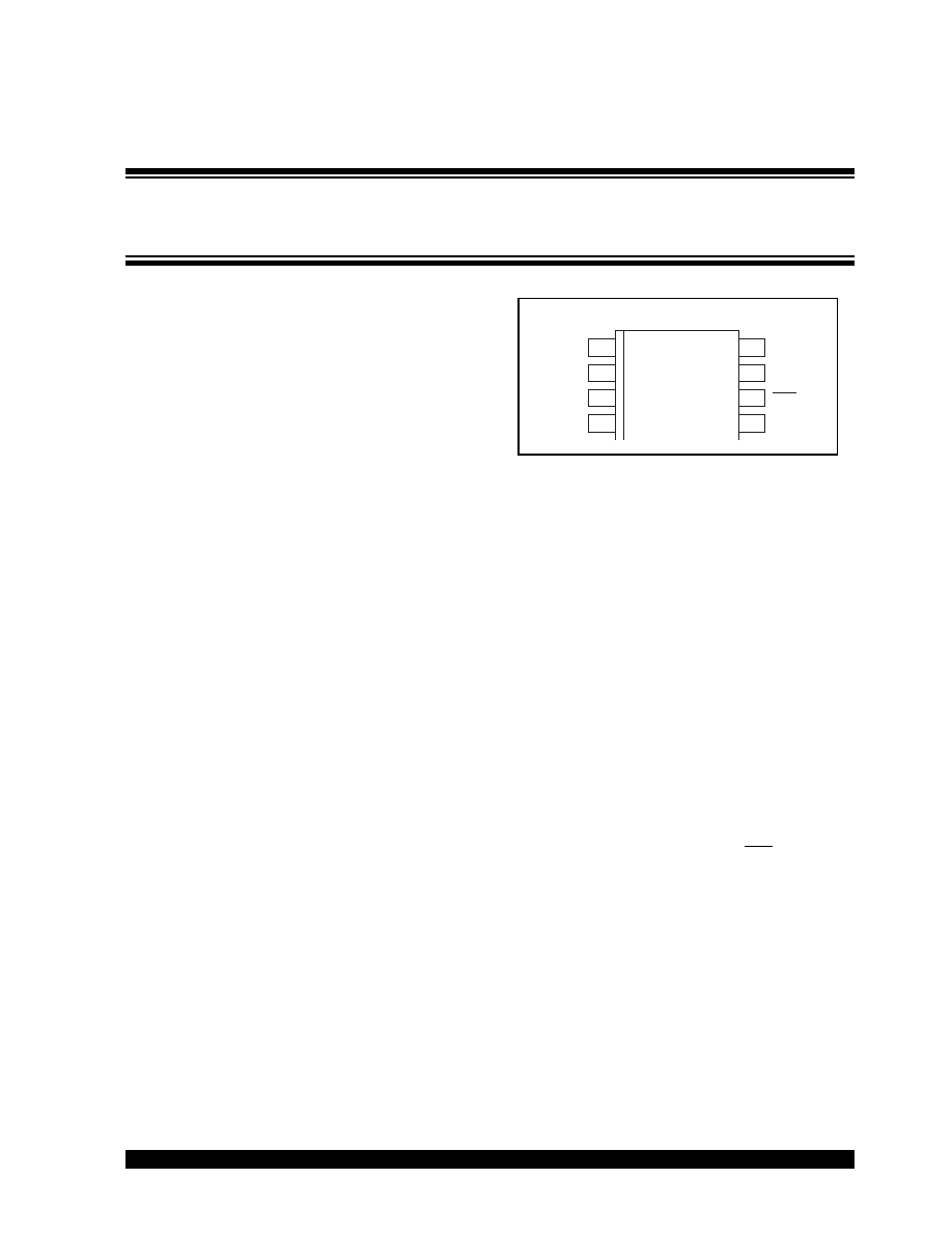
Package Types
General Description
The TC648 is a switch mode, fan speed controller for
use with brushless DC fans. Temperature proportional
speed control is accomplished using pulse width mod-
ulation (PWM). A thermistor (or other voltage output
temperature sensor) connected to the V
IN
input
furnishes the required control voltage of 1.25V to 2.65V
(typical) for 0% to 100% PWM duty cycle. The TC648
can be configured to operate in either auto-shutdown or
minimum speed mode. In auto-shutdown mode, fan
operation is automatically suspended when measured
temperature (V
IN
) is lower than a user programmed
minimum setting (V
AS
). The fan is automatically
restarted, and proportional speed control restored,
when V
IN
exceeds V
AS
(plus hysteresis). Operation in
minimum speed mode is similar to auto-shutdown
mode, with the exception that the fan is operated at a
user programmed minimum setting when the mea-
sured temperature is low. An integrated Start-up Timer
ensures reliable motor start-up at turn-on, and when
coming out of shutdown or auto-shutdown mode.
The over-temperature fault output (OTF) is asserted
when the PWM reaches 100% duty cycle, indicating a
possible thermal runaway situation.
The TC648 is available in the 8-pin plastic DIP, SOIC
and MSOP packages and is available in the industrial
and extended commercial temperature ranges.
1
8
2
7
3
6
4
5
TC648
GND
C
F
V
IN
V
AS
OTF
NC
V
DD
V
OUT
SOIC/PDIP/MSOP
Fan Speed Controller with Auto-Shutdown
and Over-Temperature Alert
TC648
DS21448C-page 2
2002 Microchip Technology Inc.
Functional Block Diagram
OTF
SHDN
NC
PWM
OTF
GND
V
AS
V
SHDN
V
IN
C
F
V
DD
V
OUT
TC648
Control
Logic
+
V
OTF
+
+
+
Start-up
Timer
Clock
Generator
2002 Microchip Technology Inc.
DS21448C-page 3
TC648
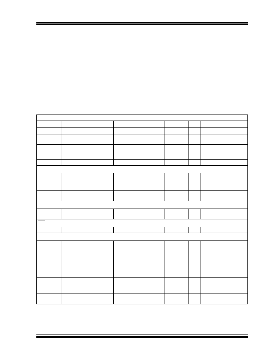
1.0
ELECTRICAL
CHARACTERISTICS
Absolute Maximum Ratings*
Supply Voltage ......................................................... 6V
Input Voltage, Any Pin... (GND 0.3V) to (V
DD
+ 0.3V)
Package Thermal Resistance:
PDIP (R
JA
)............................................. 125°C/W
SOIC (R
JA
) ............................................155°C/W
MSOP (R
JA
) .......................................... 200°C/W
Specified Temperature Range ........... -40°C to +125°C
Storage Temperature Range.............. -65°C to +150°C
*Stresses above those listed under "Absolute Maximum Rat-
ings" may cause permanent damage to the device. These are
stress ratings only and functional operation of the device at
these or any other conditions above those indicated in the
operation sections of the specifications is not implied. Expo-
sure to absolute maximum rating conditions for extended peri-
ods may affect device reliability.
DC ELECTRICAL SPECIFICATIONS
Electrical Characteristics: Unless otherwise specified, T
MIN
T
A
T
MAX
, V
DD
= 3.0V to 5.5V
Symbol
Parameter
Min
Typ
Max
Units
Test Conditions
V
DD
Supply Voltage
3.0
--
5.5
V
I
DD
Supply Current, Operating
--
0.5
1.0
mA
Pins 6, 7 Open,
C
F
= 1 µF, V
IN
= V
C(MAX)
I
DD(SHDN)
Supply Current, Shutdown/
Auto-shutdown Mode
--
25
--
µA
Pins 6, 7 Open;
Note 1
C
F
=1 µF, V
IN
= 0.35V
I
IN
V
IN
,
V
AS
Input Leakage
-1.0
--
+1.0
µA
Note 1
V
OUT
Output
t
R
V
OUT
Rise Time
--
--
50
µsec I
OH
= 5 mA, Note 1
t
F
V
OUT
Fall Time
--
--
50
µsec I
OL
= 1 mA, Note 1
I
OL
Sink Current at V
OUT
Output
1.0
--
--
mA
V
OL
= 10% of V
DD
I
OH
Source Current at V
OUT
Output
5.0
--
--
mA
V
OH
= 80% of V
DD
SENSE Input
V
TH(SENSE)
SENSE Input Threshold
Voltage with Respect to GND
50
70
90
mV
Note 1
OTF Output
V
OL
Output Low Voltage
--
--
0.3
V
I
OL
= 2.5 mA
V
IN
, V
AS
Inputs
V
C(MAX),
V
OTF
Voltage at V
IN
for 100% Duty
Cycle and Overtemp. Fault
2.5
2.65
2.8
V
V
C(SPAN)
V
C(MAX)
- V
C(MIN)
1.3
1.4
1.5
V
V
AS
Auto-shutdown Threshold
V
C(MAX) ~
V
C(SPAN)
--
V
C(MAX)
V
V
SHDN
Voltage Applied to V
IN
to
Ensure Reset/Shutdown
--
--
V
DD
x 0.13
V
V
REL
Voltage Applied to V
IN
to
Release Reset Mode
V
DD
x 0.19
--
--
V
V
DD
= 5V
V
HYST
Hysteresis on V
SHDN,
V
REL
--
0.01 x V
DD
--
V
V
HAS
Hysteresis on Auto-shutdown
Comparator
--
70
--
mV
Note 1:
Ensured by design, not tested.
TC648
DS21448C-page 4
2002 Microchip Technology Inc.
Pulse Width Modulator
F
OSC
PWM Frequency
26
30
34
Hz
C
F
= 1.0 µF
t
STARTUP
Start-up Timer
--
32/F
--
Sec
C
F
= 1.0 µF
DC ELECTRICAL SPECIFICATIONS (CONTINUED)
Electrical Characteristics: Unless otherwise specified, T
MIN
T
A
T
MAX
, V
DD
= 3.0V to 5.5V
Symbol
Parameter
Min
Typ
Max
Units
Test Conditions
Note 1:
Ensured by design, not tested.
2002 Microchip Technology Inc.
DS21448C-page 5
TC648
2.0
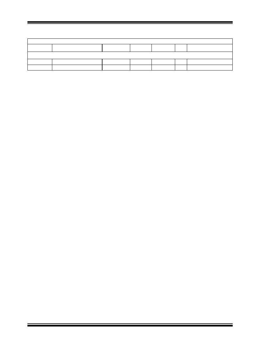
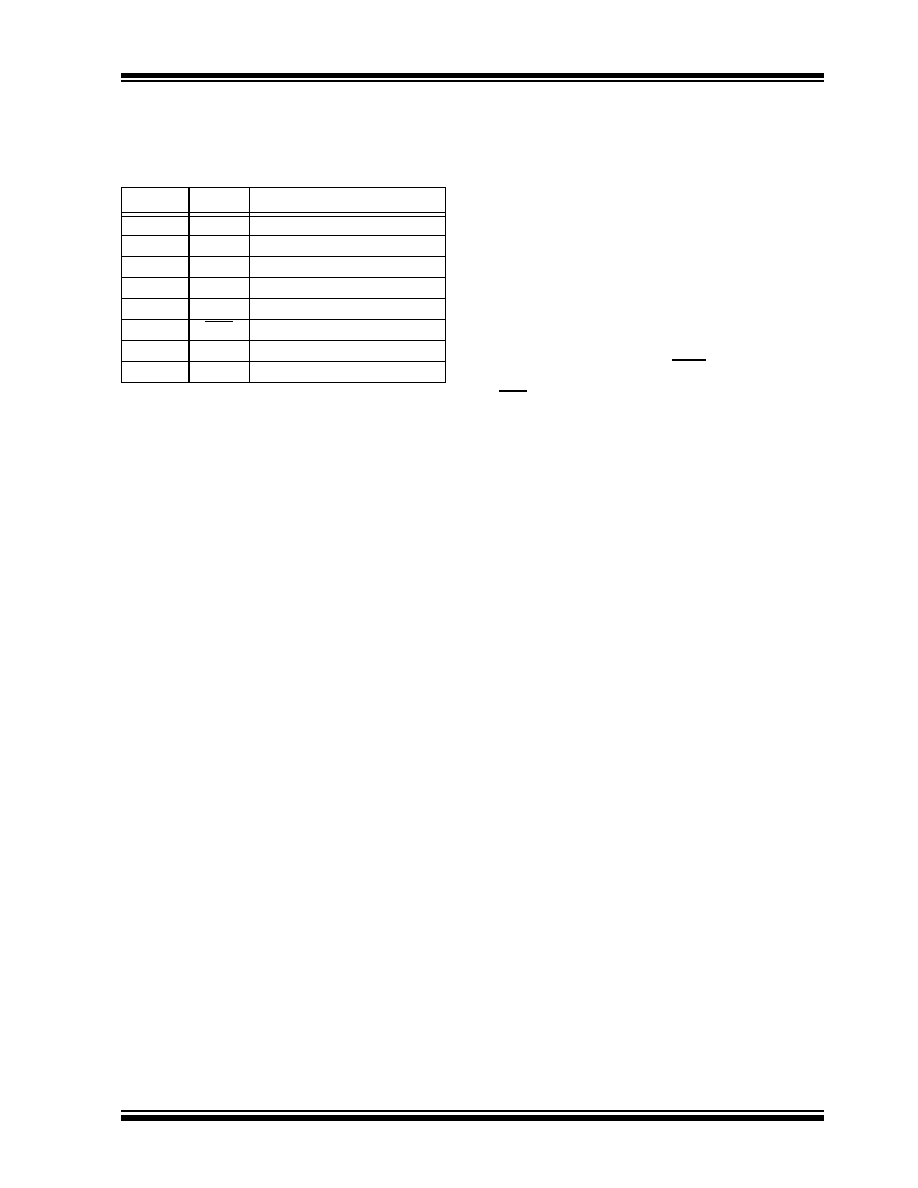
PIN DESCRIPTIONS
The descriptions of the pins are listed in Table 2-1.
TABLE 2-1:
PIN FUNCTION TABLE
2.1
Analog Input (V
IN
)
The thermistor network (or other temperature sensor)
connects to the V
IN
input. A voltage range of 1.25V to
2.65V (typical) on this pin drives an active duty cycle of
0% to 100% on the V
OUT
pin (see Section 5.0, "Typical
Applications", for more details).
2.2
Analog Output (C
F
)
C
F
is the positive terminal for the PWM ramp generator
timing capacitor. The recommended C
F
is 1 µF for
30 Hz PWM operation.
2.3
Analog Input (V
AS
)
An external resistor divider connected to the V
AS
input
sets the auto-shutdown threshold. Auto-shutdown
occurs when V
IN
V
AS
. During shutdown, supply
current falls to 25 µA (typical). The fan is automatically
restarted when V
IN
(V
AS
+V
HAS
) (see Section 5.0,
"Typical Applications" for more details).
2.4
Ground (GND)
GND denotes the ground Terminal.
2.5
No Connect
No internal connection.
2.6
Digital Output (OTF)
OTF goes low to indicate an over-temperature
condition. This occurs when the voltage at V
IN
> V
OTF
(see Section 1.0, "Electrical Characteristics"). An over-
temperature indication is a non-latching condition.
2.7
Digital Output (V
OUT
)
V
OUT
is an active high complimentary output that drives
the base of an external NPN transistor (via an appropri-
ate base resistor) or the gate of an N-channel MOS-
FET. This output has asymmetrical drive (see
Section 1.0, "Electrical Characteristics").
2.8
Power Supply Input (V
DD
)
V
DD
may be independent of the fan's power supply
(see Section 1.0, "Electrical Characteristics").
Pin No.
Symbol
Description
1
V
IN
Analog Input
2
C
F
Analog Output
3
V
AS
Analog Input
4
GND
Ground Terminal
5
NC
No Internal Connection
6
OTF
Digital (Open Collector) Output
7
V
OUT
Digital Output
8
V
DD
Power Supply Input
Document Outline