 | ÐлекÑÑоннÑй компоненÑ: TC665EUN | СкаÑаÑÑ:  PDF PDF  ZIP ZIP |
Äîêóìåíòàöèÿ è îïèñàíèÿ www.docs.chipfind.ru
2002 Microchip Technology Inc.
DS21737A-page 1
M
TC664/TC665
Features
· Temperature Proportional Fan Speed for Reduced
Acoustic Noise and Longer Fan Life
· FanSenseTM Protects against Fan Failure and
Eliminates the Need for 3-wire Fans
· Over Temperature Detection (TC665)
· Efficient PWM Fan Drive
· Provides RPM Data
· 2-Wire SMBusTM-Compatible Interface
· Supports Any Fan Voltage
· Software Controlled Shutdown Mode for "Green"
Systems
· Supports Low Cost NTC/PTC Thermistors
· Space Saving 10-Pin MSOP Package
· Temperature Range: -40°C to +85ºC
Applications
· Personal Computers & Servers
· LCD Projectors
· Datacom & Telecom Equipment
· Fan Trays
· File Servers
· Workstations
· General Purpose Fan Speed Control
Package Type
Description
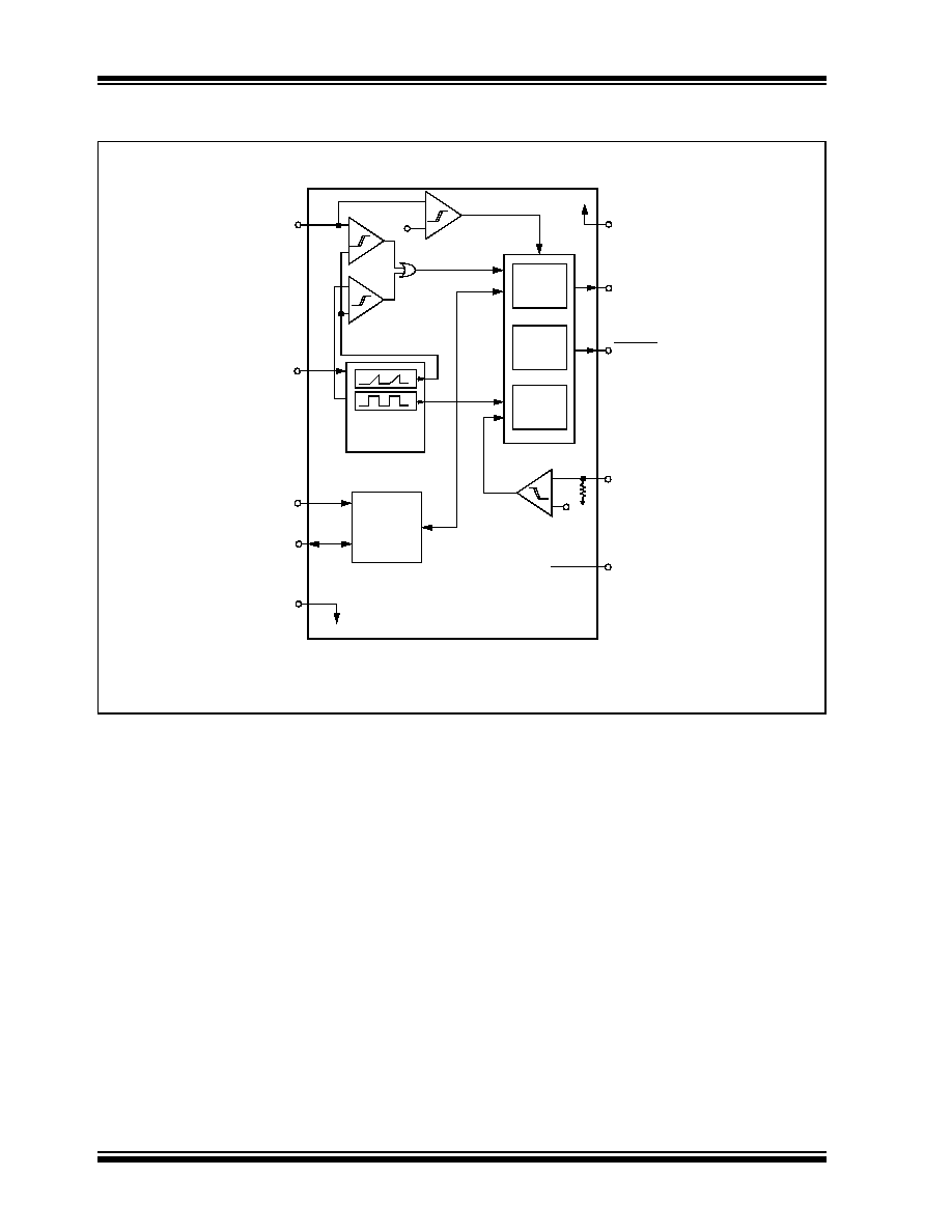
The TC664/TC665 devices are PWM mode fan speed
controllers with FanSense technology for use with
brushless DC fans. These devices implement temper-
ature proportional fan speed control which lowers
acoustic fan noise and increases fan life. The voltage
at V
IN
(Pin 1) represents temperature and is typically
provided by an external thermistor or voltage output
temperature sensor. The PWM output (V
OUT
) is
adjusted between 30% and 100%, based on the volt-
age at V
IN
. The PWM duty cycle can also be pro-
grammed via SMBus to allow fan speed control without
the need for an external thermistor. If V
IN
is not con-
nected, the TC664/TC665 will start driving the fan at a
default duty cycle of 39.33%. See Section 4.3, "Fan
Startup", for more details).
In normal fan operation, a pulse train is present at the
SENSE pin (Pin 8). The TC664/TC665 use these
pulses to calculate the fan revolutions per minute
(RPM). The fan RPM data is used to detect a worn out,
stalled, open or unconnected fan. An RPM level below
the user-programmable threshold causes the TC664/
TC665 to assert a logic low alert signal (FAULT). The
default threshold value is 500 RPM. Also, if this condi-
tion occurs, FF (bit 0<0>) in the Status Register will also
be set to a `
1
'.
An over-temperature condition is indicated when the
voltage at V
IN
exceeds 2.6 V (typical). The TC664/
TC665 devices indicate this by setting OTF(bit 5<X>) in
the Status Register to a '
1
'. The TC665 device also
pulls the FAULT line low during an over-temperature
condition.
The TC664/TC665 devices are available in a 10-Pin
MSOP package and consume 150 µA during opera-
tion. The devices can also enter a low-power shutdown
mode (5 µA, typ.) by setting the appropriate bit in the
Configuration Register. The operating temperature
range for these devices is -40°C to +85ºC.
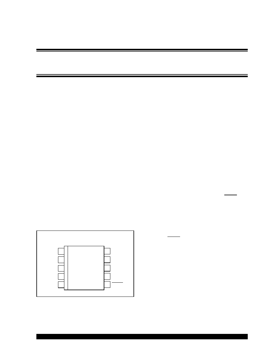
10-Pin MSOP
1
2
3
4
5
10
9
8
7
6
V
IN
C
F
SCLK
SDA
GND
V
DD
V
OUT
SENSE
NC
FAULT
TC664
TC665
SMBusTM PWM Fan Speed Controllers With
Fan Fault Detection
SMBus is a trademark of Intel Coporation
TC664/TC665
DS21737A-page 2
2002 Microchip Technology Inc.
Functional Block Diagram
V
OTF
50 k
OTF
V
MIN
TC664/TC665
SENSE
FAULT
V
OUT
V
DD
GND
SDA
SCLK
C
F
V
IN
+
+
Clock
Generator
Serial Port
Interface
Control
Logic
Start-up
Timer
Missing
Pulse
Detect
100 mV (typ.)
+
NC
+
Note: OTF condition applies for the TC665 device only.
Note
2002 Microchip Technology Inc.
DS21737A-page 3
TC664/TC665
1.0
ELECTRICAL
CHARACTERISTICS
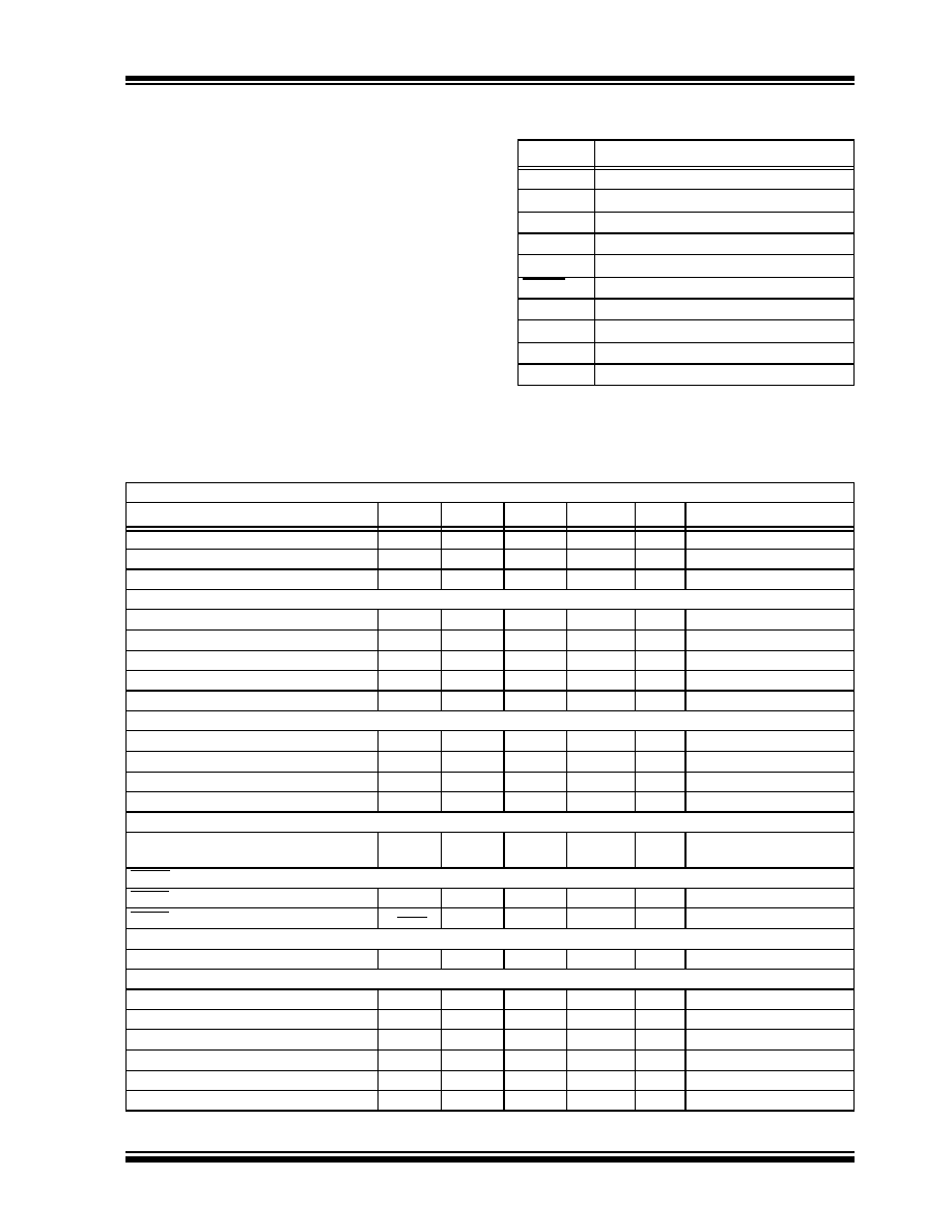
Absolute Maximum Ratings *
V
DD
..................................................................................6.5 V
Input Voltages .................................... -0.3 V to (V
DD
+ 0.3 V)
Output Voltages ................................. -0.3 V to (V
DD
+ 0.3 V)
Storage temperature .....................................-65°C to +150°C
Ambient temp. with power applied ................-40°C to +125°C
Maximum Junction Temperature, T
J
............................. 150°C
ESD protection on all pins
..................................................
4 kV
*Notice: Stresses above those listed under "Maximum rat-
ings" may cause permanent damage to the device. This is a
stress rating only and functional operation of the device at
those or any other conditions above those indicated in the
operational listings of this specification is not implied. Expo-
sure to maximum rating conditions for extended periods may
affect device reliability.
PIN FUNCTION TABLE
ELECTRICAL SPECIFICATIONS
Name
Function
V
IN
Analog Input
C
F
Analog Output
SCLK
Serial Clock Input
SDA
Serial Data In/Out (Open Drain)
GND
Ground
FAULT
Digital (Open Drain) Output
NC
No Connection
SENSE
Analog Input
V
OUT
Digital Output
V
DD
Power Supply Input
Electrical Characteristics: Unless otherwise noted, all limits are specified for V
DD
= 3.0 V to 5.5 V, -40°C <T
A
< +85°C.
Parameters
Sym
Min
Typ
Max
Units
Conditions
Supply Voltage
V
DD
3.0
--
5.5
V
Operating Supply Current
I
DD
--
150
300
µA
Pins 8, 9 Open
Shutdown Mode Supply Current
I
DDSHDN
--
5
10
µA
Pins 8, 9 Open
V
OUT
PWM Output
V
OUT
Rise Time
t
R
--
--
50
µsec
I
OH
= 5 mA, Note 1
V
OUT
Fall Time
t
F
--
--
50
µsec
I
OL
= 1 mA, Note 1
Sink Current at V
OUT
Output
I
OL
1.0
--
--
mA
V
OL
= 10% of V
DD
Source Current at V
OUT
Output
I
OH
5.0
--
--
mA
V
OH
= 80% of V
DD
PWM Frequency
F
26
30
34
Hz
C
F
= 1 µF
V
IN
Input
V
IN
Input Voltage for 100% PWM duty-cycle V
C(MAX)
2.45
2.6
2.75
V
V
C(MAX)
- V
C(MIN)
V
CRANGE
1.25
1.4
1.55
V
V
IN
Input Resistance
--
10M
--
V
DD
= 5.0 V
V
IN
Input Leakage Current
I
IN
-1.0
--
+1.0
µA
SENSE Input
SENSE Input Threshold Voltage with
Respect to GND
V
THSENSE
80
100
120
mV
FAULT Output
FAULT Output LOW Voltage
V
OL
--
--
0.3
V
I
OL
= 2.5 mA
FAULT Output Response Time
t
FAULT
--
2.4
--
sec
Fan RPM-to-Digital Output
Fan RPM ERROR
-15
--
+15
%
RPM > 1600
2-Wire Serial Bus Interface
Logic Input High
V
IH
2.1
--
--
V
Note 2
Logic Input Low
V
IL
--
--
0.8
V
Logic Output Low
V
OL
--
--
0.4
V
I
OL
= 3 mA
Input Capacitance SDA, SCLK
C
IN
--
10
15
pF
Note 1
I/O Leakage Current
I
LEAK
-1.0
--
+1.0
µA
SDA Output Low Current
I
OLSDA
6
--
--
mA
V
OL
= 0.6 V
Note 1: Not production tested, ensured by design, tested during characterization.
2: For 5.0 V < V
DD
5.5 V, the limit for V
IH
= 2.2 V.
TC664/TC665
DS21737A-page 4
2002 Microchip Technology Inc.
TEMPERATURE SPECIFICATIONS
TIMING SPECIFICATIONS
Electrical Characteristics: Unless otherwise noted, all parameters apply at V
DD
= 3.0 V to 5.5 V
Parameters
Symbol
Min
Typ
Max
Units
Conditions
Temperature Ranges:
Specified Temperature Range
T
A
-40
--
+85
°C
Operating Temperature Range
T
A
-40
--
+125
°C
Storage Temperature Range
T
A
-65
--
+150
°C
Thermal Package Resistances:
Thermal Resistance, 10 Pin MSOP
JA
--
113
--
°C/W
Electrical Characteristics: Unless otherwise noted, all limits are specified for V
DD
= 3.0 V to 5.5 V,
-40°C <T
A
< +85°C
Parameters
Sym
Min
Typ
Max
Units
Conditions
SMBus Interface (See Figure 1-1)
Serial Port Frequency
f
SC
0
--
100
kHz
Note 1
Low Clock Period
t
LOW
4.7
--
--
µsec Note 1
High Clock Period
t
HIGH
4.7
--
--
µsec Note 1
SCLK and SDA Rise Time
t
R
--
--
1000
nsec Note 1
SCLK and SDA Fall Time
t
F
--
--
300
nsec Note 1
Start Condition Setup Time
t
SU(START)
4.7
--
--
µsec Note 1
SCLK Clock Period Time
t
SC
10
--
--
µsec Note 1
Start Condition Hold Time
t
H(START)
4.0
--
--
µsec Note 1
Data in SetupTime to SCLK
High
t
SU-DATA
250
--
--
nsec Note 1
Data in Hold Time after SCLK
Low
t
H-DATA
300
--
--
nsec Note 1
Stop Condition Setup Time
t
SU(STOP)
4.0
--
--
µsec Note 1
Bus Free Time Prior to New
Transition
t
IDLE
4.7
--
µsec Note 1 and Note 2
Note 1: Not production tested, ensured by design, tested during characterization.
2: Time the bus must be free before a new transmission can start.
2002 Microchip Technology Inc.
DS21737A-page 5
TC664/TC665
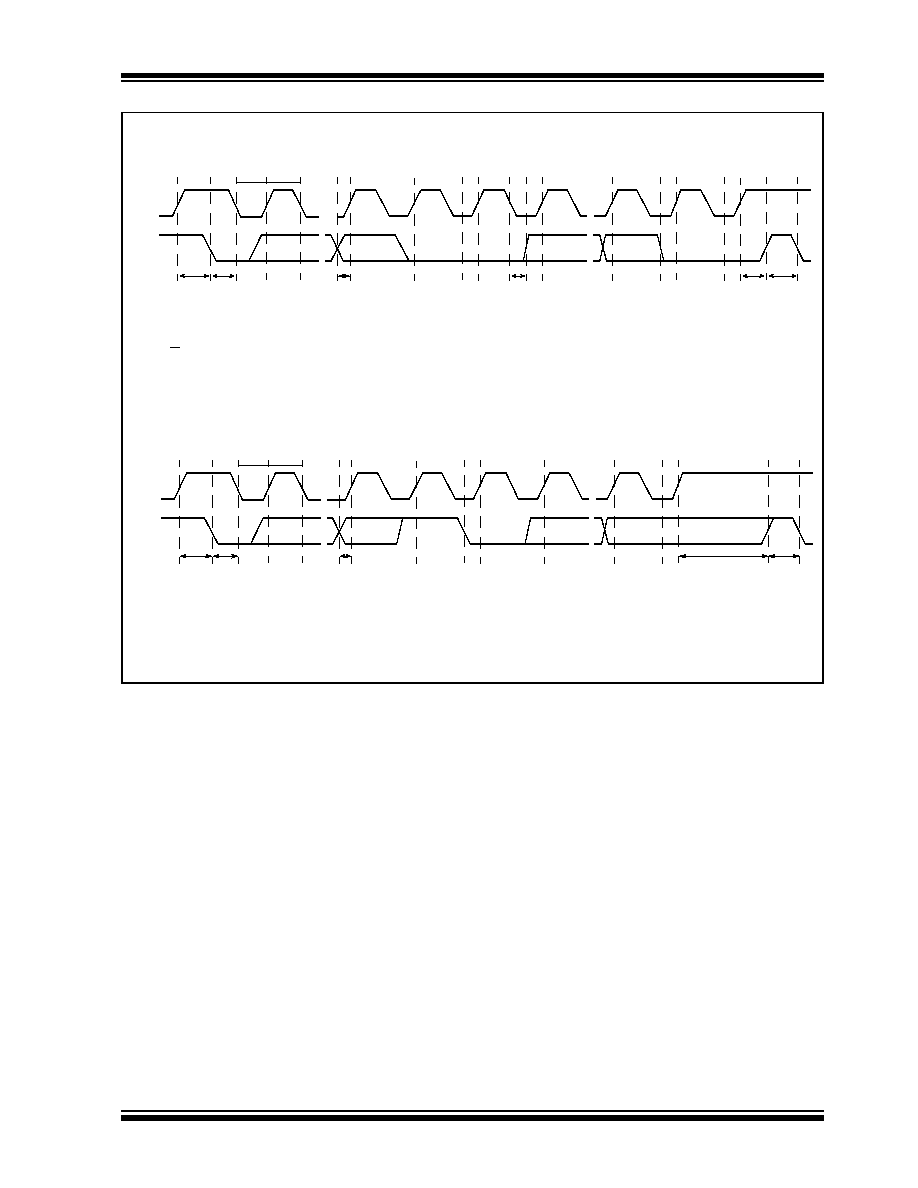
FIGURE 1-1:
Bus Timing Data.
t
SU(START)
t
H(START)
t
SU-DATA
t
SU(STOP)
t
IDLE
A = Start Condition
B = MSB of Address Clocked into Slave
C = LSB of Address Clocked into Slave
D = R/W Bit Clocked into Slave
E = Slave Pulls SDA Line Low
A
B
C
D
E
F
G
H
I J
K
L
M
F = Acknowledge Bit Clocked into Master
G = MSB of Data Clocked into Slave
H = LSB of Data Clocked into Slave
I = Slave Pulls SDA Line Low
J = Acknowledge Clocked into Master
K = Acknowledge Clock Pulse
L = Stop Condition, Data Executed by Slave
M = New Start Condition
t
LOW
t
HIGH
SCLK
SDA
t
H-DATA
SMBus Write Timing Diagram
t
SU(START)
t
H(START)
t
SU-DATA
t
SU(STOP)
t
IDLE
A = Start Condition
B = MSB of Address Clocked into Slave
C = LSB of Address Clocked into Slave
D = R/W Bit Clocked into Slave
A
B
C
D
E F
G
H
I
J
K
E = Slave Pulls SDA Line Low
F = Acknowledge Bit Clocked into Master
G = MSB of Data Clocked into Master
H = LSB of Data Clocked into Master
t
LOW
t
HIGH
I = Acknowledge Clock Pulse
J = Stop Condition
K = New Start Condition
SCLK
SDA
SMBus Read Timing Diagram
E
Document Outline