 | –≠–ª–µ–∫—Ç—Ä–æ–Ω–Ω—ã–π –∫–æ–º–ø–æ–Ω–µ–Ω—Ç: TC7116IJL | –°–∫–∞—á–∞—Ç—å:  PDF PDF  ZIP ZIP |

©
2002 Microchip Technology Inc.
DS21457B-page 1
TC7116/A/TC7117/A
Features
∑ Low Temperature Drift Internal Reference
- TC7116/TC7117 80 ppm/∞C Typ.
- TC7116A/TC7117A 20 ppm/∞C Typ.
∑ Display Hold Function
∑ Directly Drives LCD or LED Display
∑ Zero Reading with Zero Input
∑ Low Noise for Stable Display
- 2V or 200mV Full Scale Range (FSR)
∑ Auto-Zero Cycle Eliminates Need for Zero
∑ Adjustment Potentiometer
∑ True Polarity Indication for Precision Null
Applications
∑ Convenient 9V Battery Operation:
(TC7116/TC7116A)
∑ High Impedance CMOS Differential Inputs: 10
12
∑ Low Power Operation: 10mW
Applications
∑ Thermometry
∑ Bridge Readouts: Strain Gauges, Load Cells,
Null Detectors
∑ Digital Meters: Voltage/Current/Ohms/Power, pH
∑ Digital Scales, Process Monitors
∑ Portable Instrumentation
Device Selection Table
General Description
The TC7116A/TC7117A are 3-1/2 digit CMOS analog-
to-digital converters (ADCs) containing all the active
components necessary to construct a 0.05% resolution
measurement
system.
Seven-segment
decoders,
polarity and digit drivers, voltage reference, and clock
circuit are integrated on-chip. The TC7116A drives liq-
uid crystal displays (LCDs) and includes a backplane
driver. The TC7117A drives common anode light emit-
ting diode (LED) displays directly with an 8mA drive
current per segment.
These devices incorporate a display hold (HLDR) func-
tion. The displayed reading remains indefinitely, as
long as HLDR is held high. Conversions continue, but
output data display latches are not updated. The refer-
ence low input (V
REF
-) is not available, as it is with the
TC7106/7107. V
REF
- is tied internally to analog com-
mon in the TC7116A/7117A devices.
The TC7116A/7117A reduces linearity error to less
than 1 count. Rollover error (the difference in readings
for equal magnitude but opposite polarity input signals)
is below ±1 count. High-impedance differential inputs
offer 1pA leakage current and a 10
12
input imped-
ance. The 15
µ
V
P-P
noise performance enables a "rock
solid" reading. The auto-zero cycle ensures a zero dis-
play reading with a 0V input.
The TC7116A and TC7117A feature a precision, low
drift internal reference, and are functionally identical to
the TC7116/TC7117. A low drift external reference is
not normally required with the TC7116A/TC7117A.
Package Code
Package
Temperature Range
CPL
40-Pin PDIP
0
∞
C to +70
∞
C
IJL
40-Pin CERDIP
-25
∞
C to +85
∞
C
CKW
44-Pin PQFP
0
∞
C to +70
∞
C
CLW
44-Pin PLCC
0
∞
C to +70
∞
C
3-1/2 Digit Analog-to-Digital Converters with Hold
TC7116/A/TC7117/A
DS21457B-page 2
©
2002 Microchip Technology Inc.
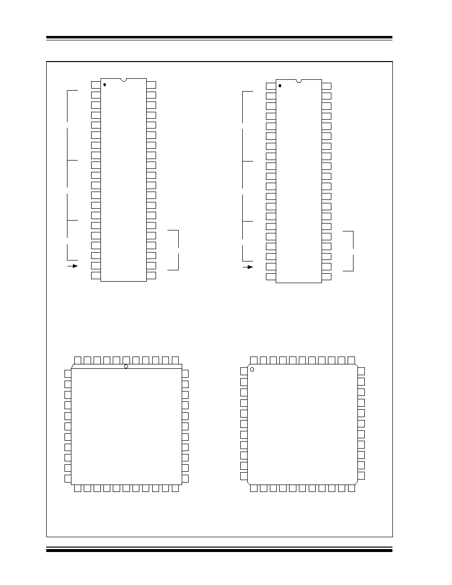
Package Type
BP/
GND
33
34
35
36
37
38
39
13
10
9
8
7
COMMON
V+
18 19 20 21
23 24
AB
4
POL
NC
V
IN
+
NC
V
IN
-
B2
6
5
4
3
1 44
2
A
1
OSC1
22
43
OSC2
42
OSC3
41
TEST
40
V
REF
+
25 26 27 28
F
3
E
3
G
3
A
3
C
3
G
2
32
14
C
AZ
31
15
V
BUFF
30
16
V
INT
E
2
29
17
D
3
NC
11
12
NC
C
2
D
2
F
2
A
2
B
3
TC7116CLW
TC7116ACLW
TC7117CLW
TC7117ACLW
TC7116CPL
TC7116ACPL
TC7117CPL
TC7117ACPL
V-
C
REF
+
C
REF
-
B
1
C
1
D
1
F
1
G
1
E
1
BP/
GND
27
28
29
30
31
32
33
7
4
3
2
1
NC
TC7116CKW
TC7116ACKW
TC7117CKW
TC7117ACKW
12 13 14 15
17 18
G
3
44 43 42 41
39 38
40
V
REF
+
COMMON
16
37
C
AZ
36
V
BUFF
35
V
INT
34
V-
19 20 21 22
D
3
26
8
25
9
24
10
23
11
V
IN
+
5
6
C
3
OSC3
TEST
NC
NC
HLDR
D
2
C
2
B
2
A
2
F
2
E
2
NC
OSC2
OSC1
V+
C
REF
+
C
REF
-
V
IN
-
A
3
G
3
POL
AB
4
E
3
F
3
B
3
D
1
C
1
B
1
A
1
F
1
G
1
E
1
40-Pin PDIP
40-Pin CERDIP
44-Pin PLCC
44-Pin PQFP
1
2
3
4
OSC1
5
6
7
8
9
10
11
12
TEST
V
REF
+
COMMON
C
AZ
HLDR
D
2
13
14
15
16
17
18
19
20
40
39
38
37
36
35
34
33
32
31
30
29
28
27
26
25
24
23
22
21
C
2
B
2
A
2
F
2
E
2
D
3
B
3
F
3
E
3
AB
4
(Minus Sign)
(Minus Sign)
10's
100's
1000's
(TC7116/7117)
(TC7116A/TC7117A)
(TC7116/7117)
(TC7116A/TC7117A)
100's
OSC2
OSC3
V+
C
REF
+
C
REF
-
V
IN
+
V
IN
-
V
BUFF
V
INT
V-
G
2
C
3
A
3
G
3
BP/GND
POL
D
1
C
1
B
1
A
1
F
1
G
1
E
1
1's
HLDR
TC7116IJL
TC7116AIJL
TC7117IJL
TC7117AIJL
1
2
3
4
OSC1
5
6
7
8
9
10
11
12
TEST
V
REF
+
COMMON
C
AZ
HLDR
D
2
13
14
15
16
17
18
19
20
40
39
38
37
36
35
34
33
32
31
30
29
28
27
26
25
24
23
22
21
C
2
B
2
A
2
F
2
E
2
D
3
B
3
F
3
E
3
AB
4
10's
100's
1000's
100's
OSC2
OSC3
V+
C
REF
+
C
REF
-
V
IN
+
V
IN
-
V
BUFF
V
INT
V-
G
2
C
3
A
3
G
3
BP/GND
POL
D
1
C
1
B
1
A
1
F
1
G
1
E
1
1's
Note
1: NC = No internal connection.
2: Pins 9, 25, 40 and 56 are connected to the die substrate. The potential at these pins is approximately V+. No external
connections should be made.

©
2002 Microchip Technology Inc.
DS21457B-page 3
TC7116/A/TC7117/A
Typical Application
V
REF
+
TC7116/A
9V
V
REF
33
34
24k
1k
31
29
36
39
38
40
0.47
µF
0.1
µF
V-
OSC1
OSC3
OSC2
To Analog
Common (Pin 32)
3 Conversions Per Second
C
OSC
100k
47k
0.22
µF
0.01
µF
Analog
Input
+
≠
C
REF
-
C
REF
+
V
IN
+
V
IN
-
ANALOG
COMMON
V
INT
V
BUFF
C
AZ
20
21
35
Segment
Drive
2≠19
22≠25
POL
BP/GND
V+
Minus Sign
Backplane Drive
28
R
OSC
100pF
LCD Display (TC7116/7116A)
or Common Anode LED Display
(TC7117/7117A)
1M
27
30
32
HLDR
Display
Hold
100mV
1
26
TC7117/A
+

TC7116/A/TC7117/A
DS21457B-page 4
©
2002 Microchip Technology Inc.
1.0
ELECTRICAL
CHARACTERISTICS
Absolute Maximum Ratings*
Supply Voltage:
TC7116/TC7116A (V+ to V-) ........................... 15V
TC7117/TC7117A (V+ to GND) .......................+6V
V- to GND.........................................................-9V
Analog Input Voltage (Either Input) (Note 1) ... V+ to V-
Reference Input Voltage (Either Input) ............ V+ to V-
Clock Input:
TC7116/TC7116A............................... TEST to V+
TC7117/TC7117A.................................GND to V+
Package Power Dissipation; T
A
70∞C (Note 2)
40-Pin CDIP ................................................2.29W
40-Pin PDIP ................................................1.23W
44-Pin PLCC ...............................................1.23W
44-Pin PQFP ...............................................1.00W
Operating Temperature:
C (Commercial) Device ................... 0∞C to +70∞C
I (Commercial) Device.................... 0∞C to +70∞C
Storage Temperature.......................... -65∞C to +150∞C
*Stresses above those listed under "Absolute Maximum
Ratings" may cause permanent damage to the device. These
are stress ratings only and functional operation of the device
at these or any other conditions above those indicated in the
operation sections of the specifications is not implied.
Exposure to Absolute Maximum Rating conditions for
extended periods may affect device reliability.
TC7116/A AND TC7117/A ELECTRICAL SPECIFICATIONS
Electrical Characteristics: Unless otherwise noted, specifications apply to both the TC7116/A and TC7117/A at T
A
= 25∞C,
f
CLOCK
= 48kHz. Parts are tested in the circuit of the Typical Operating Circuit.
Symbol
Parameter
Min
Typ
Max
Unit
Test Conditions
Z
IR
Zero Input Reading
--
±0
--
Digital
Reading
V
IN
= 0V
Full Scale = 200mV
Ratiometric Reading
999
999/1000
1000
Digital
Reading
V
IN
= V
REF
V
REF
= 100mV
R/O
Rollover Error (Difference in Reading for
Equal Positive and Negative
Readings Near Full Scale)
-1
±0.2
+1
Counts
V
IN
- = + V
IN
+
200mV
or
2V
Linearity (Maximum Deviation from Best
Straight Line Fit)
-1
±0.2
+1
Counts
Full Scale = 200mV or 2V
CMRR
Common Mode Rejection Ratio
(Note 3)
--
50
--
µ
V/V
V
CM
= ±1V, V
IN
= 0V
Full Scale = 200mV
e
N
Noise (Peak to Peak 95% of Time)
--
15
--
µ
V
V
IN
= 0V
Full Scale = 200mV
I
L
Leakage Current at Input
--
1
10
pA
V
IN
= 0V
Zero Reading Drift
--
0.2
1
µ
V/∞C
V
IN
= 0V
"C" Device = 0∞C to +70∞C
--
1.0
2
µ
V/∞C
"I" Device = -25∞C to +85∞C
Note
1:
Input voltages may exceed the supply voltages provided the input current is limited to ±100
µ
A.
2:
Dissipation rating assumes device is mounted with all leads soldered to printed circuit board.
3:
Refer to "Differential Input" discussion.
4:
Backplane drive is in phase with segment drive for "OFF" segment, 180∞ out of phase for "ON" segment. Frequency is
20 times conversion rate. Average DC component is less than 50mV.
5:
The TC7116/TC7116A logic inputs have an internal pull-down resistor connected from HLDR, Pin 1 to TEST, Pin 37. The
TC7117/TC7117A logic inputs have an internal pull-down resistor connected from HLDR, Pin 1 to GND, Pin 21.

©
2002 Microchip Technology Inc.
DS21457B-page 5
TC7116/A/TC7117/A
TC
SF
Scale Factor Temperature Coefficient
--
1
5
ppm/∞C
V
IN
= 199mV,
"C" Device = 0∞C to +70∞C
(Ext. Ref = 0ppm∞C)
--
--
20
ppm/∞C
"I" Device = -25∞C to +85∞C
Input Resistance, Pin 1
30
70
--
k
(Note 5)
V
IL,
Pin 1
--
--
Test + 1.5
V
TC7116/A Only
V
IL,
Pin 1
--
--
GND + 1.5
V
TC7117/A Only
V
IH,
Pin 1
V
+
- 1.5
--
--
V
Both
I
DD
Supply Current (Does not Include LED
Current for TC7117/A)
--
0.8
1.8
mA
V
IN
= 0V
V
C
Analog Common Voltage
(with Respect to Positive Supply)
2.4
3.05
3.35
V
25k
Between Common
and Positive Supply
V
CTC
Temperature Coefficient of Analog
Common (with Respect to Positive
Supply)
--
--
20
80
--
50
--
--
ppm/∞C
ppm/∞C
"C" Device: 0∞C to
+70∞C
TC7116A/TC7117A
TC7116/TC7117
V
SD
TC7116/TC7117A ONLY Peak to Peak
Segment Drive Voltage
4
5
6
V
V+ to V- = 9V
(Note 4)
V
BD
TC7116A/TC7116A ONLY Peak to Peak
Backplane Drive Voltage
4
5
6
V
V+ to V- = 9V
(Note 4)
TC7117/TC7117A ONLY
Segment Sinking Current
(Except Pin 19)
5
8
--
mA
V+ = 5.0V
Segment Voltage = 3V
TC7117/TC7117A ONLY
Segment Sinking Current (Pin 19 Only)
10
16
--
mA
V+ = 5.0V
Segment Voltage = 3V
TC7116/A AND TC7117/A ELECTRICAL SPECIFICATIONS (CONTINUED)
Electrical Characteristics: Unless otherwise noted, specifications apply to both the TC7116/A and TC7117/A at T
A
= 25∞C,
f
CLOCK
= 48kHz. Parts are tested in the circuit of the Typical Operating Circuit.
Symbol
Parameter
Min
Typ
Max
Unit
Test Conditions
Note
1:
Input voltages may exceed the supply voltages provided the input current is limited to ±100
µ
A.
2:
Dissipation rating assumes device is mounted with all leads soldered to printed circuit board.
3:
Refer to "Differential Input" discussion.
4:
Backplane drive is in phase with segment drive for "OFF" segment, 180∞ out of phase for "ON" segment. Frequency is
20 times conversion rate. Average DC component is less than 50mV.
5:
The TC7116/TC7116A logic inputs have an internal pull-down resistor connected from HLDR, Pin 1 to TEST, Pin 37. The
TC7117/TC7117A logic inputs have an internal pull-down resistor connected from HLDR, Pin 1 to GND, Pin 21.