3 1/2 Digit Analog-to-Digital Converters with Hold
©
2002 Microchip Technology Inc.
DS21457B-page 1
TC7116/A/TC7117/A
Features
· Low Temperature Drift Internal Reference
- TC7116/TC7117 80 ppm/°C Typ.
- TC7116A/TC7117A 20 ppm/°C Typ.
· Display Hold Function
· Directly Drives LCD or LED Display
· Zero Reading with Zero Input
· Low Noise for Stable Display
- 2V or 200mV Full Scale Range (FSR)
· Auto-Zero Cycle Eliminates Need for Zero
· Adjustment Potentiometer
· True Polarity Indication for Precision Null
Applications
· Convenient 9V Battery Operation:
(TC7116/TC7116A)
· High Impedance CMOS Differential Inputs: 10
12
· Low Power Operation: 10mW
Applications
· Thermometry
· Bridge Readouts: Strain Gauges, Load Cells,
Null Detectors
· Digital Meters: Voltage/Current/Ohms/Power, pH
· Digital Scales, Process Monitors
· Portable Instrumentation
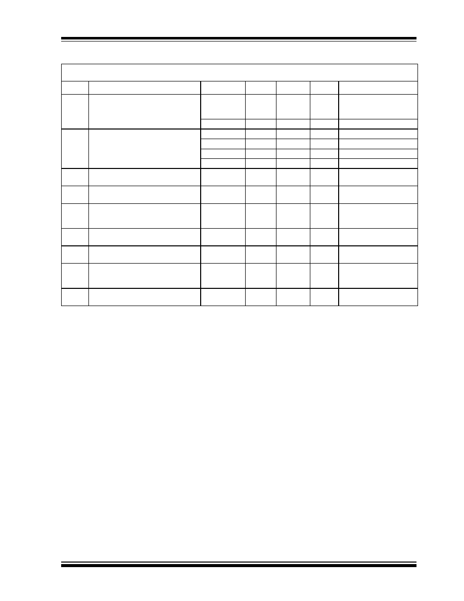
Device Selection Table
General Description
The TC7116A/TC7117A are 3-1/2 digit CMOS analog-
to-digital converters (ADCs) containing all the active
components necessary to construct a 0.05% resolution
measurement
system.
Seven-segment
decoders,
polarity and digit drivers, voltage reference, and clock
circuit are integrated on-chip. The TC7116A drives liq-
uid crystal displays (LCDs) and includes a backplane
driver. The TC7117A drives common anode light emit-
ting diode (LED) displays directly with an 8mA drive
current per segment.
These devices incorporate a display hold (HLDR) func-
tion. The displayed reading remains indefinitely, as
long as HLDR is held high. Conversions continue, but
output data display latches are not updated. The refer-
ence low input (V
REF
-) is not available, as it is with the
TC7106/7107. V
REF
- is tied internally to analog com-
mon in the TC7116A/7117A devices.
The TC7116A/7117A reduces linearity error to less
than 1 count. Rollover error (the difference in readings
for equal magnitude but opposite polarity input signals)
is below ±1 count. High-impedance differential inputs
offer 1pA leakage current and a 10
12
input imped-
ance. The 15
µ
V
P-P
noise performance enables a "rock
solid" reading. The auto-zero cycle ensures a zero dis-
play reading with a 0V input.
The TC7116A and TC7117A feature a precision, low
drift internal reference, and are functionally identical to
the TC7116/TC7117. A low drift external reference is
not normally required with the TC7116A/TC7117A.
Package Code
Package
Temperature Range
CPL
40-Pin PDIP
0
°
C to +70
°
C
IJL
40-Pin CERDIP
-25
°
C to +85
°
C
CKW
44-Pin PQFP
0
°
C to +70
°
C
CLW
44-Pin PLCC
0
°
C to +70
°
C
3-1/2 Digit Analog-to-Digital Converters with Hold
TC7116/A/TC7117/A
DS21457B-page 2
©
2002 Microchip Technology Inc.
Package Type
BP/
GND
33
34
35
36
37
38
39
13
10
9
8
7
COMMON
V+
18 19 20 21
23 24
AB
4
POL
NC
V
IN
+
NC
V
IN
-
B2
6
5
4
3
1 44
2
A
1
OSC1
22
43
OSC2
42
OSC3
41
TEST
40
V
REF
+
25 26 27 28
F
3
E
3
G
3
A
3
C
3
G
2
32
14
C
AZ
31
15
V
BUFF
30
16
V
INT
E
2
29
17
D
3
NC
11
12
NC
C
2
D
2
F
2
A
2
B
3
TC7116CLW
TC7116ACLW
TC7117CLW
TC7117ACLW
TC7116CPL
TC7116ACPL
TC7117CPL
TC7117ACPL
V-
C
REF
+
C
REF
-
B
1
C
1
D
1
F
1
G
1
E
1
BP/
GND
27
28
29
30
31
32
33
7
4
3
2
1
NC
TC7116CKW
TC7116ACKW
TC7117CKW
TC7117ACKW
12 13 14 15
17 18
G
3
44 43 42 41
39 38
40
V
REF
+
COMMON
16
37
C
AZ
36
V
BUFF
35
V
INT
34
V-
19 20 21 22
D
3
26
8
25
9
24
10
23
11
V
IN
+
5
6
C
3
OSC3
TEST
NC
NC
HLDR
D
2
C
2
B
2
A
2
F
2
E
2
NC
OSC2
OSC1
V+
C
REF
+
C
REF
-
V
IN
-
A
3
G
3
POL
AB
4
E
3
F
3
B
3
D
1
C
1
B
1
A
1
F
1
G
1
E
1
40-Pin PDIP
40-Pin CERDIP
44-Pin PLCC
44-Pin PQFP
1
2
3
4
OSC1
5
6
7
8
9
10
11
12
TEST
V
REF
+
COMMON
C
AZ
HLDR
D
2
13
14
15
16
17
18
19
20
40
39
38
37
36
35
34
33
32
31
30
29
28
27
26
25
24
23
22
21
C
2
B
2
A
2
F
2
E
2
D
3
B
3
F
3
E
3
AB
4
(Minus Sign)
(Minus Sign)
10's
100's
1000's
(TC7116/7117)
(TC7116A/TC7117A)
(TC7116/7117)
(TC7116A/TC7117A)
100's
OSC2
OSC3
V+
C
REF
+
C
REF
-
V
IN
+
V
IN
-
V
BUFF
V
INT
V-
G
2
C
3
A
3
G
3
BP/GND
POL
D
1
C
1
B
1
A
1
F
1
G
1
E
1
1's
HLDR
TC7116IJL
TC7116AIJL
TC7117IJL
TC7117AIJL
1
2
3
4
OSC1
5
6
7
8
9
10
11
12
TEST
V
REF
+
COMMON
C
AZ
HLDR
D
2
13
14
15
16
17
18
19
20
40
39
38
37
36
35
34
33
32
31
30
29
28
27
26
25
24
23
22
21
C
2
B
2
A
2
F
2
E
2
D
3
B
3
F
3
E
3
AB
4
10's
100's
1000's
100's
OSC2
OSC3
V+
C
REF
+
C
REF
-
V
IN
+
V
IN
-
V
BUFF
V
INT
V-
G
2
C
3
A
3
G
3
BP/GND
POL
D
1
C
1
B
1
A
1
F
1
G
1
E
1
1's
Note
1: NC = No internal connection.
2: Pins 9, 25, 40 and 56 are connected to the die substrate. The potential at these pins is approximately V+. No external
connections should be made.
©
2002 Microchip Technology Inc.
DS21457B-page 3
TC7116/A/TC7117/A
Typical Application
V
REF
+
TC7116/A
9V
V
REF
33
34
24k
1k
31
29
36
39
38
40
0.47
µF
0.1
µF
V-
OSC1
OSC3
OSC2
To Analog
Common (Pin 32)
3 Conversions Per Second
C
OSC
100k
47k
0.22
µF
0.01
µF
Analog
Input
+
C
REF
-
C
REF
+
V
IN
+
V
IN
-
ANALOG
COMMON
V
INT
V
BUFF
C
AZ
20
21
35
Segment
Drive
219
2225
POL
BP/GND
V+
Minus Sign
Backplane Drive
28
R
OSC
100pF
LCD Display (TC7116/7116A)
or Common Anode LED Display
(TC7117/7117A)
1M
27
30
32
HLDR
Display
Hold
100mV
1
26
TC7117/A
+
TC7116/A/TC7117/A
DS21457B-page 4
©
2002 Microchip Technology Inc.
1.0
ELECTRICAL
CHARACTERISTICS
Absolute Maximum Ratings*
Supply Voltage:
TC7116/TC7116A (V+ to V-) ........................... 15V
TC7117/TC7117A (V+ to GND) .......................+6V
V- to GND.........................................................-9V
Analog Input Voltage (Either Input) (Note 1) ... V+ to V-
Reference Input Voltage (Either Input) ............ V+ to V-
Clock Input:
TC7116/TC7116A............................... TEST to V+
TC7117/TC7117A.................................GND to V+
Package Power Dissipation; T
A
70°C (Note 2)
40-Pin CDIP ................................................2.29W
40-Pin PDIP ................................................1.23W
44-Pin PLCC ...............................................1.23W
44-Pin PQFP ...............................................1.00W
Operating Temperature:
C (Commercial) Device ................... 0°C to +70°C
I (Commercial) Device.................... 0°C to +70°C
Storage Temperature.......................... -65°C to +150°C
*Stresses above those listed under "Absolute Maximum
Ratings" may cause permanent damage to the device. These
are stress ratings only and functional operation of the device
at these or any other conditions above those indicated in the
operation sections of the specifications is not implied.
Exposure to Absolute Maximum Rating conditions for
extended periods may affect device reliability.
TC7116/A AND TC7117/A ELECTRICAL SPECIFICATIONS
Electrical Characteristics: Unless otherwise noted, specifications apply to both the TC7116/A and TC7117/A at T
A
= 25°C,
f
CLOCK
= 48kHz. Parts are tested in the circuit of the Typical Operating Circuit.
Symbol
Parameter
Min
Typ
Max
Unit
Test Conditions
Z
IR
Zero Input Reading
--
±0
--
Digital
Reading
V
IN
= 0V
Full Scale = 200mV
Ratiometric Reading
999
999/1000
1000
Digital
Reading
V
IN
= V
REF
V
REF
= 100mV
R/O
Rollover Error (Difference in Reading for
Equal Positive and Negative
Readings Near Full Scale)
-1
±0.2
+1
Counts
V
IN
- = + V
IN
+
200mV
or
2V
Linearity (Maximum Deviation from Best
Straight Line Fit)
-1
±0.2
+1
Counts
Full Scale = 200mV or 2V
CMRR
Common Mode Rejection Ratio
(Note 3)
--
50
--
µ
V/V
V
CM
= ±1V, V
IN
= 0V
Full Scale = 200mV
e
N
Noise (Peak to Peak 95% of Time)
--
15
--
µ
V
V
IN
= 0V
Full Scale = 200mV
I
L
Leakage Current at Input
--
1
10
pA
V
IN
= 0V
Zero Reading Drift
--
0.2
1
µ
V/°C
V
IN
= 0V
"C" Device = 0°C to +70°C
--
1.0
2
µ
V/°C
"I" Device = -25°C to +85°C
Note
1:
Input voltages may exceed the supply voltages provided the input current is limited to ±100
µ
A.
2:
Dissipation rating assumes device is mounted with all leads soldered to printed circuit board.
3:
Refer to "Differential Input" discussion.
4:
Backplane drive is in phase with segment drive for "OFF" segment, 180° out of phase for "ON" segment. Frequency is
20 times conversion rate. Average DC component is less than 50mV.
5:
The TC7116/TC7116A logic inputs have an internal pull-down resistor connected from HLDR, Pin 1 to TEST, Pin 37. The
TC7117/TC7117A logic inputs have an internal pull-down resistor connected from HLDR, Pin 1 to GND, Pin 21.
©
2002 Microchip Technology Inc.
DS21457B-page 5
TC7116/A/TC7117/A
TC
SF
Scale Factor Temperature Coefficient
--
1
5
ppm/°C
V
IN
= 199mV,
"C" Device = 0°C to +70°C
(Ext. Ref = 0ppm°C)
--
--
20
ppm/°C
"I" Device = -25°C to +85°C
Input Resistance, Pin 1
30
70
--
k
(Note 5)
V
IL,
Pin 1
--
--
Test + 1.5
V
TC7116/A Only
V
IL,
Pin 1
--
--
GND + 1.5
V
TC7117/A Only
V
IH,
Pin 1
V
+
- 1.5
--
--
V
Both
I
DD
Supply Current (Does not Include LED
Current for TC7117/A)
--
0.8
1.8
mA
V
IN
= 0V
V
C
Analog Common Voltage
(with Respect to Positive Supply)
2.4
3.05
3.35
V
25k
Between Common
and Positive Supply
V
CTC
Temperature Coefficient of Analog
Common (with Respect to Positive
Supply)
--
--
20
80
--
50
--
--
ppm/°C
ppm/°C
"C" Device: 0°C to
+70°C
TC7116A/TC7117A
TC7116/TC7117
V
SD
TC7116/TC7117A ONLY Peak to Peak
Segment Drive Voltage
4
5
6
V
V+ to V- = 9V
(Note 4)
V
BD
TC7116A/TC7116A ONLY Peak to Peak
Backplane Drive Voltage
4
5
6
V
V+ to V- = 9V
(Note 4)
TC7117/TC7117A ONLY
Segment Sinking Current
(Except Pin 19)
5
8
--
mA
V+ = 5.0V
Segment Voltage = 3V
TC7117/TC7117A ONLY
Segment Sinking Current (Pin 19 Only)
10
16
--
mA
V+ = 5.0V
Segment Voltage = 3V
TC7116/A AND TC7117/A ELECTRICAL SPECIFICATIONS (CONTINUED)
Electrical Characteristics: Unless otherwise noted, specifications apply to both the TC7116/A and TC7117/A at T
A
= 25°C,
f
CLOCK
= 48kHz. Parts are tested in the circuit of the Typical Operating Circuit.
Symbol
Parameter
Min
Typ
Max
Unit
Test Conditions
Note
1:
Input voltages may exceed the supply voltages provided the input current is limited to ±100
µ
A.
2:
Dissipation rating assumes device is mounted with all leads soldered to printed circuit board.
3:
Refer to "Differential Input" discussion.
4:
Backplane drive is in phase with segment drive for "OFF" segment, 180° out of phase for "ON" segment. Frequency is
20 times conversion rate. Average DC component is less than 50mV.
5:
The TC7116/TC7116A logic inputs have an internal pull-down resistor connected from HLDR, Pin 1 to TEST, Pin 37. The
TC7117/TC7117A logic inputs have an internal pull-down resistor connected from HLDR, Pin 1 to GND, Pin 21.
TC7116/A/TC7117/A
DS21457B-page 6
©
2002 Microchip Technology Inc.
2.0
PIN DESCRIPTIONS
The descriptions of the pins are listed in Table 2-1.
TABLE 2-1:
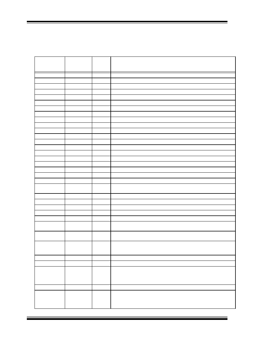
PIN FUNCTION TABLE
Pin Number
(40-Pin PDIP)
(40-Pin CERDIP)
Pin Number
(44-Pin PQFP)
Symbol
Description
1
8
HLDR
Hold pin, Logic 1 holds present display reading.
2
9
D
1
Activates the D section of the units display.
3
10
C
1
Activates the C section of the units display.
4
11
B
1
Activates the B section of the units display.
5
12
A
1
Activates the A section of the units display.
6
13
F
1
Activates the F section of the units display.
7
14
G
1
Activates the G section of the units display.
8
15
E
1
Activates the E section of the units display.
9
16
D
2
Activates the D section of the tens display.
10
17
C
2
Activates the C section of the tens display.
11
18
B
2
Activates the B section of the tens display.
12
19
A
2
Activates the A section of the tens display.
13
20
F
2
Activates the F section of the tens display.
14
21
E
2
Activates the E section of the tens display.
15
22
D
3
Activates the D section of the hundreds display.
16
23
B
3
Activates the B section of the hundreds display.
17
24
F
3
Activates the F section of the hundreds display.
18
25
E
3
Activates the E section of the hundreds display.
19
26
AB
4
Activates both halves of the 1 in the thousands display.
20
27
POL
Activates the negative polarity display.
21
28
BP/
GND
LCD backplane drive output (TC7116/TC7116A). Digital ground
(TC7117/TC7117A).
22
29
G
3
Activates the G section of the hundreds display.
23
30
A
3
Activates the A section of the hundreds display.
24
31
C
3
Activates the C section of the hundreds display.
25
32
G
2
Activates the G section of the tens display.
26
34
V-
Negative power supply voltage.
27
35
V
INT
Integrator output. Connection point for integration capacitor.
See Section 4.3, Integrating Capacitor for more details.
28
36
V
BUFF
Integration resistor connection. Use a 47k
resistor for a 200mV full scale range
and a 470k
resistor for 2V full scale range.
29
37
C
AZ
The size of the auto-zero capacitor influences system noise. Use a 0.47
µ
F
capacitor for 200mV full scale, and a 0.047
µ
F capacitor for 2V full scale.
See Section 4.1, Auto-Zero Capacitor for more details.
30
38
V
IN
-
The analog LOW input is connected to this pin.
31
39
V
IN
+
The analog HIGH input signal is connected to this pin.
32
40
COMMON This pin is primarily used to set the Analog Common mode voltage for battery
operation, or in systems where the input signal is referenced to the power supply.
It also acts as a reference voltage source. See Section 3.1.6, Analog Common
for more details.
33
41
C
REF
-
See Pin 34.
34
42
C
REF
+
A 0.1
µ
F capacitor is used in most applications. If a large Common mode voltage
exists (for example, the V
IN
- pin is not at analog common), and a 200mV scale is
used, a 1
µ
F capacitor is recommended and will hold the rollover error to
0.5 count.
©
2002 Microchip Technology Inc.
DS21457B-page 7
TC7116/A/TC7117/A
3.0
DETAILED DESCRIPTION
(All Pin Designations Refer to 40-Pin PDIP.)
3.1
Analog Section
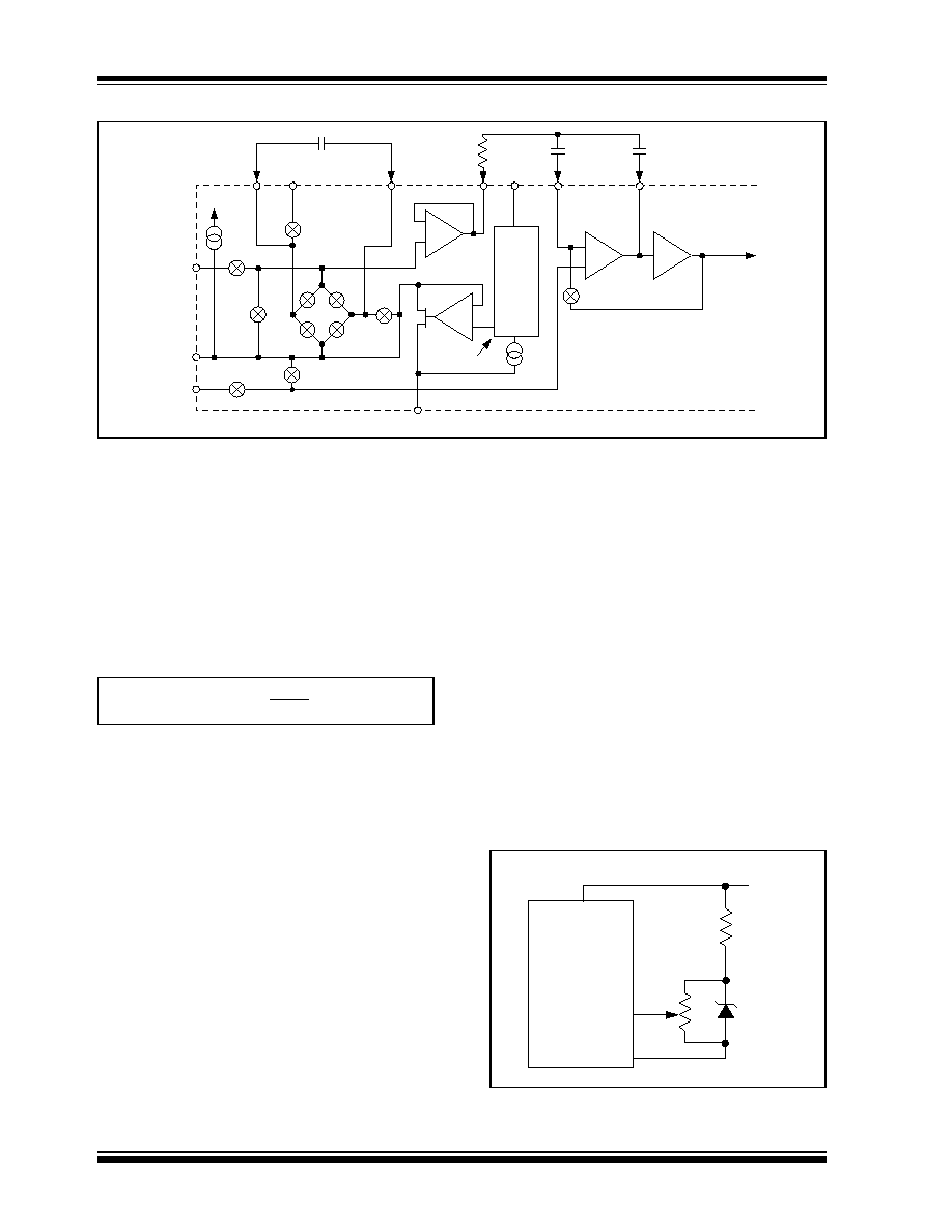
Figure 3-1 shows the block diagram of the analog sec-
tion for the TC7116/TC7116A and TC7117/TC7117A.
Each measurement cycle is divided into three phases:
(1) Auto-Zero (AZ), (2) Signal Integrate (INT), and
(3) Reference Integrate (REF), or De-integrate (DE).
3.1.1
AUTO-ZERO PHASE
High and low inputs are disconnected from the pins and
internally shorted to analog common. The reference
capacitor is charged to the reference voltage. A feed-
back loop is closed around the system to charge the
auto-zero capacitor (C
AZ
) to compensate for offset volt-
ages in the buffer amplifier, integrator, and comparator.
Since the comparator is included in the loop, AZ accu-
racy is limited only by system noise. The offset referred
to the input is less than 10
µ
V.
3.1.2
SIGNAL INTEGRATE PHASE
The auto-zero loop is opened, the internal short is
removed, and the internal high and low inputs are con-
nected to the external pins. The converter then inte-
grates the differential voltages between V
IN
+ and V
IN
-
for a fixed time. This differential voltage can be within a
wide Common mode range: 1V of either supply. How-
ever, if the input signal has no return with respect to the
converter power supply, V
IN
- can be tied to analog
common to establish the correct Common mode volt-
age. At the end of this phase, the polarity of the
integrated signal is determined
.
35
43
V+
Positive Power Supply Voltage.
36
44
V
REF
+
The analog input required to generate a full scale output (1999 counts). Place
100mV between Pins 32 and 36 for 199.9mV full scale. Place 1V between
Pins 35 and 36 for 2V full scale. See Section 4.6, Reference Voltage.
37
3
TEST
Lamp test. When pulled HIGH (to V+), all segments will be turned on and the dis-
play should read -1888. It may also be used as a negative supply for externally
generated decimal points. See Section 3.1.7, TEST for additional information.
38
4
OSC3
See Pin 40.
39
6
OSC2
See Pin 40.
40
7
OSC1
Pins 40, 39, 38 make up the oscillator section. For a 48kHz clock (3 readings per
section), connect Pin 40 to the junction of a 100k
resistor and a 100pF capaci-
tor. The 100k
resistor is tied to Pin 39 and the 100pF capacitor is tied to Pin 38.
TABLE 2-1:
PIN FUNCTION TABLE (CONTINUED)
Pin Number
(40-Pin PDIP)
(40-Pin CERDIP)
Pin Number
(44-Pin PQFP)
Symbol
Description
TC7116/A/TC7117/A
DS21457B-page 8
©
2002 Microchip Technology Inc.
FIGURE 3-1:
ANALOG SECTION OF TC7116/TC7117A AND TC7117/TC7117A
3.1.3
REFERENCE INTEGRATE PHASE
The final phase is reference integrate, or de-integrate.
Input low is internally connected to analog common
and input high is connected across the previously
charged reference capacitor. Circuitry within the chip
ensures that the capacitor will be connected with the
correct polarity to cause the integrator output to return
to zero. The time required for the output to return to
zero is proportional to the input signal. The digital
reading displayed is:
EQUATION 3-1:
3.1.4
REFERENCE
The positive reference voltage (V
REF
+) is referred to
analog common.
3.1.5
DIFFERENTIAL INPUT
This input can accept differential voltages anywhere
within the Common mode range of the input amplifier
or, specifically, from 1V below the positive supply to 1V
above the negative supply. In this range, the system
has a CMRR of 86dB, typical. However, since the inte-
grator also swings with the Common mode voltage,
care must be exercised to ensure that the integrator
output does not saturate. A worst case condition would
be a large, positive Common mode voltage with a near
full scale negative differential input voltage. The nega-
tive input signal drives the integrator positive, when
most of its swing has been used up by the positive
Common mode voltage. For these critical applications,
the integrator swing can be reduced to less than the
recommended 2V full scale swing with little loss of
accuracy. The integrator output can swing within 0.3V
of either supply without loss of linearity.
3.1.6
ANALOG COMMON
This pin is included primarily to set the Common mode
voltage for battery operation (TC7116/TC7116A), or for
any system where the input signals are floating, with
respect to the power supply. The analog common pin
sets a voltage approximately 2.8V more negative than
the positive supply. This is selected to give a minimum
end of life battery voltage of about 6V. However, analog
common has some attributes of a reference voltage.
When the total supply voltage is large enough to cause
the zener to regulate (>7V), the analog common volt-
age will have a low voltage coefficient (0.001%), low
output impedance (
15
), and a temperature coeffi-
cient of less than 20ppm/°C, typically, and 50 ppm max-
imum. The TC7116/TC7117 temperature coefficients
are typically 80ppm/°C.
An external reference may be used, if necessary, as
shown in Figure 3-2.
FIGURE 3-2:
USING AN EXTERNAL
REFERENCE
TC7116
TC7116A
TC7117
TC7117A
C
REF
C
REF
+
C
REF
-
R
INT
V+
C
AZ
Auto-Zero
V
INT
28
35
29
27
33
36
34
10
µA
31
AZ
AZ
INT
AZ & DE (±)
32
30
INT
26
Integrator
V+ -3V
Comparator
To
Digital
Section
DE (+)
DE
()
DE
(+)
DE ()
V+
AZ
Analog
Common
V
IN
+
V
IN
-
V
BUFF
C
INT
V
REF
+
Low
Temp.
Drift
Zener
V
REF
V-
+
+
+
+
1000 =
V
IN
V
REF
V+
V+
1.2V REF
COMMON
TC7116
TC7116A
TC7117
TC7117A
6.8k
V
REF
+
20k
©
2002 Microchip Technology Inc.
DS21457B-page 9
TC7116/A/TC7117/A
Analog common is also used as V
IN
- return during
auto-zero and de-integrate. If V
IN
- is different from ana-
log common, a Common mode voltage exists in the
system and is taken care of by the excellent CMRR of
the converter. However, in some applications, V
IN
- will
be set at a fixed, known voltage (power supply common
for instance). In this application, analog common
should be tied to the same point, thus removing the
Common mode voltage from the converter. The same
holds true for the reference voltage; if it can be conve-
niently referenced to analog common, it should be.
This removes the Common mode voltage from the
reference system.
Within the IC, analog common is tied to an N-channel
FET, that can sink 30mA or more of current to hold the
voltage 3V below the positive supply (when a load is
trying to pull the analog common line positive). How-
ever, there is only 10
µ
A of source current, so analog
common may easily be tied to a more negative voltage,
thus overriding the internal reference.
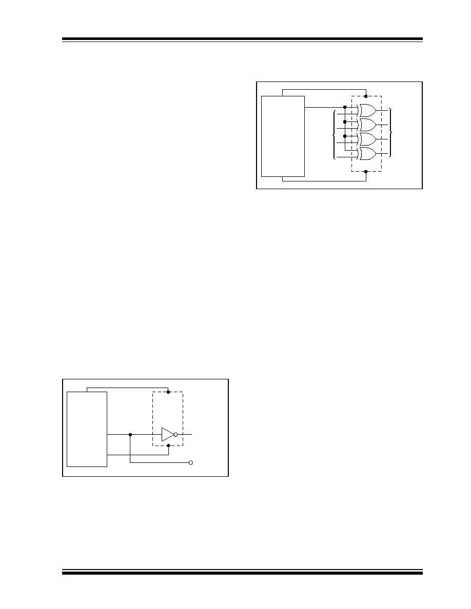
3.1.7
TEST
The TEST pin serves two functions. On the TC7117/
TC7117A, it is coupled to the internally generated digi-
tal supply through a 500
resistor. Thus, it can be used
as a negative supply for externally generated segment
drivers, such as decimal points, or any other presenta-
tion the user may want to include on the LCD.
(Figure 3-3 and Figure 3-4 show such an application.)
No more than a 1mA load should be applied.
The second function is a "lamp test." When TEST is
pulled HIGH (to V+), all segments will be turned ON
and the display should read -1888. The TEST pin will
sink about 10mA under these conditions.
FIGURE 3-3:
SIMPLE INVERTER FOR
FIXED DECIMAL POINT
FIGURE 3-4:
EXCLUSIVE "OR" GATE
FOR DECIMAL POINT
DRIVE
3.2
Digital Section
Figure 3-5 and Figure 3-6 show the digital section for
TC7116/TC7116A and TC7117/TC7117A, respectively.
For the TC7116/TC7116A (Figure 3-5), an internal dig-
ital ground is generated from a 6V zener diode and a
large P-channel source follower. This supply is made
stiff to absorb the relative large capacitive currents
when the backplane (BP) voltage is switched. The BP
frequency is the clock frequency 4800. For 3 readings
per second, this is a 60Hz square wave with a nominal
amplitude of 5V. The segments are driven at the same
frequency and amplitude, and are in phase with BP
when OFF, but out of phase when ON. In all cases,
negligible DC voltage exists across the segments.
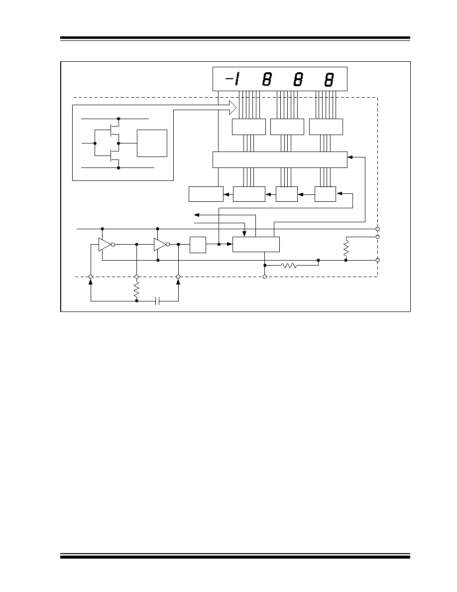
Figure 3-6 is the digital section of the TC7117/
TC7117A. It is identical to the TC7116/TC7116A,
except that the regulated supply and BP drive have
been eliminated, and the segment drive is typically
8mA. The 1000's output (Pin 19) sinks current from two
LED segments, and has a 16mA drive capability. The
TC7117/TC7117A are designed to drive common
anode LED displays.
In both devices, the polarity indication is ON for analog
inputs. If V
IN
- and V
IN
+ are reversed, this indication can
be reversed also, if desired.
TC7116
TC7116A
BP
TEST
37
21
V+
V+
GND
To LCD
Decimal
Point
To LCD
Backplane
4049
TC7116
TC7116A
Decimal
Point
Select
V+
V+
TEST
GND
4030
To LCD
Decimal
Point
BP
TC7116/A/TC7117/A
DS21457B-page 10
©
2002 Microchip Technology Inc.
FIGURE 3-5:
TC7116/TC7116A DIGITAL SECTION
3.2.1
SYSTEM TIMING
The clocking method used for the TC7116/TC7116A
and TC7117/TC7117A is shown in Figure 3-6. Three
clocking methods may be used:
1.
An external oscillator connected to Pin 40.
2.
A crystal between Pins 39 and 40.
3.
An RC network using all three pins.
The oscillator frequency is
÷
4 before it clocks the
decade counters. It is then further divided to form the
three convert cycle phases: Signal Integrate (1000
counts), Reference De-integrate (0 to 2000 counts),
and Auto-Zero (1000 to 3000 counts). For signals less
than full scale, auto-zero gets the unused portion of ref-
erence de-integrate. This makes a complete measure
cycle of 4000 (16,000 clock pulses), independent of
input voltage. For 3 readings per second, an oscillator
frequency of 48kHz would be used.
To achieve maximum rejection of 60Hz pickup, the sig-
nal integrate cycle should be a multiple of 60Hz. Oscil-
lator frequencies of 240kHz, 120kHz, 80kHz, 60kHz,
48kHz, 40kHz, etc. should be selected. For 50Hz rejec-
tion,
oscillator
frequencies
of
200kHz,
100kHz,
66-2/3kHz, 50kHz, 40kHz, etc. would be suitable. Note
that 40kHz (2.5 readings per second) will reject both
50Hz and 60Hz.
3.2.2
HOLD READING INPUT
When HLDR is at a logic HIGH, the latch will not be
updated. Analog-to-digital conversions will continue,
but will not be updated until HLDR is returned to LOW.
To continuously update the display, connect to TEST
(TC7116/TC7116A) or GROUND (TC7117/TC7117A),
or disconnect. This input is CMOS compatible with
70k
typical resistance to TEST (TC7116/TC7116A) or
GROUND (TC7117/TC7117A).
TC7116
TC7116A
LCD Phase Driver
Thousands
Hundreds
Tens
Units
4
Backplane
21
39
37
OSC2
Internal Digital Ground
V+
V-
TEST
6.2V
500
26
35
To Switch Drivers
From Comparator Output
Clock
V
TH
= 1V
7-Segment
Decode
7-Segment
Decode
7-Segment
Decode
200
40
38
Typical Segment Output
Internal Digital Ground
Segment
Output
V+
0.5mA
2mA
Latch
OSC3
OSC1
÷
÷
HLDR
~70k
Logic Control
1
©
2002 Microchip Technology Inc.
DS21457B-page 11
TC7116/A/TC7117/A
FIGURE 3-6:
TC7117/TC711A DIGITAL SECTION
TC7117
TC7117A
4
39
OSC2
V+
Digital
GND
TEST
35
Clock
40
38
OSC3
OSC1
÷
HLDR
Control Logic
Typical Segment Output
Digital Ground
To
Segment
V+
0.5mA
8mA
37
21
500
V+
1
Latch
~70k
To Switch Drivers
From Comparator Output
Internal Digital Ground
Thousands
Hundreds
Tens
Units
7-Segment
Decode
7-Segment
Decode
7-Segment
Decode
TC7116/A/TC7117/A
DS21457B-page 12
©
2002 Microchip Technology Inc.
4.0
COMPONENT VALUE
SELECTION
4.1
Auto-Zero Capacitor
The size of the auto-zero capacitor has some influence
on system noise. For 200mV full scale, where noise is
very important, a 0.47
µ
F capacitor is recommended.
On the 2V scale, a 0.047
µ
F capacitor increases the
speed of recovery from overload and is adequate for
noise on this scale.
4.2
Reference Capacitor
A 0.1
µ
F capacitor is acceptable in most applications.
However, where a large Common mode voltage exists
(i.e., the V
IN
- pin is not at analog common), and a
200mV scale is used, a larger value is required to pre-
vent rollover error. Generally, 1
µ
F will hold the rollover
error to 0.5 count in this instance.
4.3
Integrating Capacitor
The integrating capacitor should be selected to give the
maximum voltage swing that ensures tolerance buildup
will not saturate the integrator swing (approximately
0.3V from either supply). In the TC7116/TC7116A or
the TC7117/TC7117A, when the analog common is
used as a reference, a nominal ±2V full scale integrator
swing is acceptable. For the TC7117/TC7117A, with
±5V supplies and analog common tied to supply
ground, a ±3.5V to ±4V swing is nominal. For 3 read-
ings per second (48kHz clock), nominal values for C
INT
are 0.22
µ
1F and 0.10
µ
F, respectively. If different oscil-
lator frequencies are used, these values should be
changed in inverse proportion to maintain the output
swing. The integrating capacitor must have low dielec-
tric absorption to prevent rollover errors. Polypropylene
capacitors are recommended for this application.
4.4
Integrating Resistor
Both the buffer amplifier and the integrator have a class
A output stage with 100
µ
A of quiescent current. They
can supply 20
µ
A of drive current with negligible non-
linearity. The integrating resistor should be large
enough to remain in this very linear region over the
input voltage range, but small enough that undue leak-
age requirements are not placed on the PC board. For
2V full scale, 470k
is near optimum and, similarly,
47k
for 200mV full scale.
4.5
Oscillator Components
For all frequency ranges, a 100k
resistor is recom-
mended; the capacitor is selected from the equation:
EQUATION 4-1:
For a 48kHz clock (3 readings per second), C = 100pF.
4.6
Reference Voltage
To generate full scale output (2000 counts), the analog
input requirement is V
IN
= 2V
REF
. Thus, for the 200mV
and 2V scale, V
REF
should equal 100mV and 1V,
respectively. In many applications, where the ADC is
connected to a transducer, a scale factor exists
between the input voltage and the digital reading. For
instance, in a measuring system, the designer might like
to have a full scale reading when the voltage from the
transducer is 700mV. Instead of dividing the input down
to 200mV, the designer should use the input voltage
directly and select V
REF
= 350mV. Suitable values for
integrating resistor and capacitor would be 120kW and
0.22
µ
F. This makes the system slightly quieter and also
avoids a divider network on the input. The TC7117/
TC7117A, with ±5V supplies, can accept input signals
up to ±4V. Another advantage of this system is when a
digital reading of zero is desired for V
IN
0. Tempera-
ture and weighing systems with a variable tare are
examples. This offset reading can be conveniently gen-
erated by connecting the voltage transducer between
V
IN
+ and analog common, and the variable (or fixed)
offset voltage between analog common and V
IN
-.
5.0
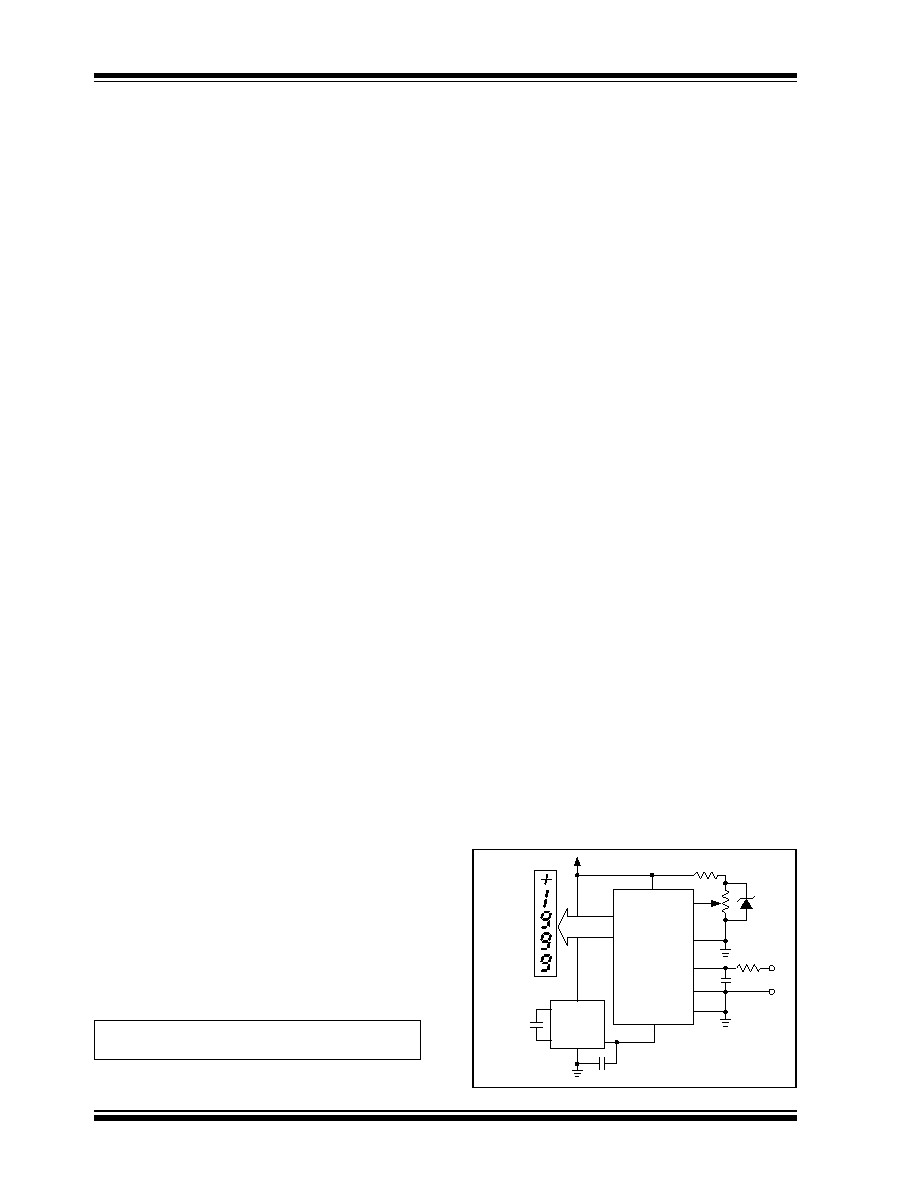
TC7117/TC7117A POWER
SUPPLIES
The TC7117/TC7117A are designed to operate from
±5V supplies. However, if a negative supply is not avail-
able, it can be generated with a TC7660 DC-to-DC con-
verter and two capacitors. Figure 5-1 shows this
application.
In selected applications, a negative supply is not
required. The conditions for using a single +5V supply
are:
1.
The input signal can be referenced to the center
of the Common mode range of the converter.
2.
The signal is less than ±1.5V.
3.
An external reference is used.
FIGURE 5-1:
NEGATIVE POWER
SUPPLY GENERATION
WITH TC7660
f
0.45
RC
-----------
=
V
REF
+
V+
TC7117
TC7117A
36
10
µF
V
IN
+
V
IN
-
COM
GND
32
31
30
21
10
µF
V
IN
V-
(-5V)
5
3
8
2
4
+5V
35
TC7660
26
+
+
+
LED
Drive
©
2002 Microchip Technology Inc.
DS21457B-page 13
TC7116/A/TC7117/A
6.0
TYPICAL APPLICATIONS
The TC7117/TC7117A sink the LED display current,
causing heat to build up in the IC package. If the inter-
nal voltage reference is used, the changing chip tem-
perature can cause the display to change reading. By
reducing the LED common anode voltage, the TC7117/
TC7117A package power dissipation is reduced.
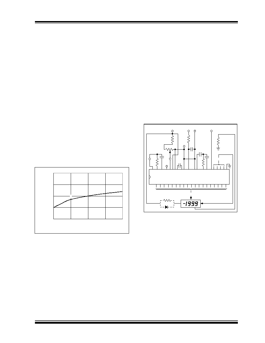
Figure 6-1 is a curve tracer display showing the rela-
tionship between output current and output voltage for
typical TC7117CPL/TC7117ACPL devices. Since a
typical LED has 1.8V across it at 8mA and its common
anode is connected to +5V, the TC7117/TC7117A out-
put is at 3.2V (Point A, Figure 6-1). Maximum power
dissipation is 8.1mA x 3.2V x 24 segments = 622mW.
However, notice that once the TC7117/TC7117A's out-
put voltage is above 2V, the LED current is essentially
constant as output voltage increases. Reducing the
output voltage by 0.7V (Point B Figure 6-1) results in
7.7mA of LED current, only a 5% reduction. Maximum
power dissipation is now only 7.7mA x 2.5V x 24 =
462mW, a reduction of 26%. An output voltage reduc-
tion of 1V (Point C) reduces LED current by 10%
(7.3mA), but power dissipation by 38% (7.3mA x 2.2V
x 24 = 385mW).
FIGURE 6-1:
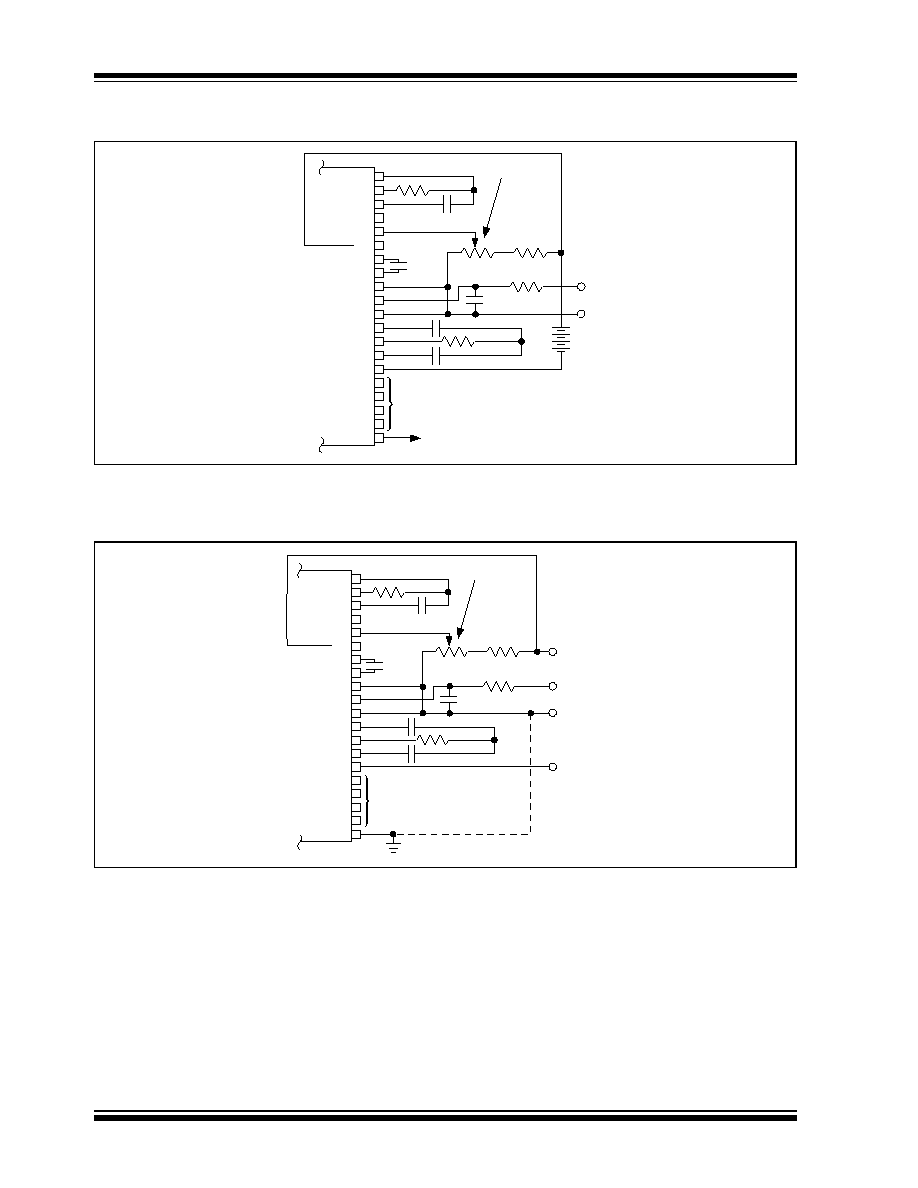
TC7117/TC7117A OUTPUT
VS. OUTPUT VOLTAGE
Reduced power dissipation is very easy to obtain.
Figure 6-2 shows two ways: either a 5.1
, 1/4W resis-
tor, or a 1A diode placed in series with the display (but
not in series with the TC7117/TC7117A). The resistor
reduces the TC7117/TC7117A's output voltage (when
all 24 segments are ON) to Point C of Figure 6-1. When
segments turn off, the output voltage will increase. The
diode, however, will result in a relatively steady output
voltage, around Point B.
In addition to limiting maximum power dissipation, the
resistor reduces change in power dissipation as the
display changes. The effect is caused by the fact that,
as fewer segments are ON, each ON output drops
more voltage and current. For the best case of six seg-
ments (a "111" display) to worst case (a "1888" display),
the resistor circuit will change about 230mW, while a
circuit without the resistor will change about 470mW.
Therefore, the resistor will reduce the effect of display
dissipation on reference voltage drift by about 50%.
The change in LED brightness caused by the resistor is
almost unnoticeable as more segments turn off. If dis-
play brightness remaining steady is very important to
the designer, a diode may be used instead of the
resistor.
FIGURE 6-2:
DIODE OR RESISTOR
LIMITS PACKAGE POWER
DISSIPATION
C
B
A
6.000
7.000
8.000
9.000
10.000
2.00
2.50
3.00
3.50
4.00
Output Voltage (V)
O
u
t
put
C
u
r
r
ent
(
m
A)
TP2
TP5
100
k
TP1
24k
1k
0.1
µF
TP3
0.01
µF
+
In
0.22
µF
Display
Display
100
pF
+5V
1M
-5V
150k
0.47
µF
TC7117
TC7117A
40
TP
4
30
35
21
20
10
1
47
k
1N4001
1.5W, 1/4
TC7116/A/TC7117/A
DS21457B-page 14
©
2002 Microchip Technology Inc.
FIGURE 6-3:
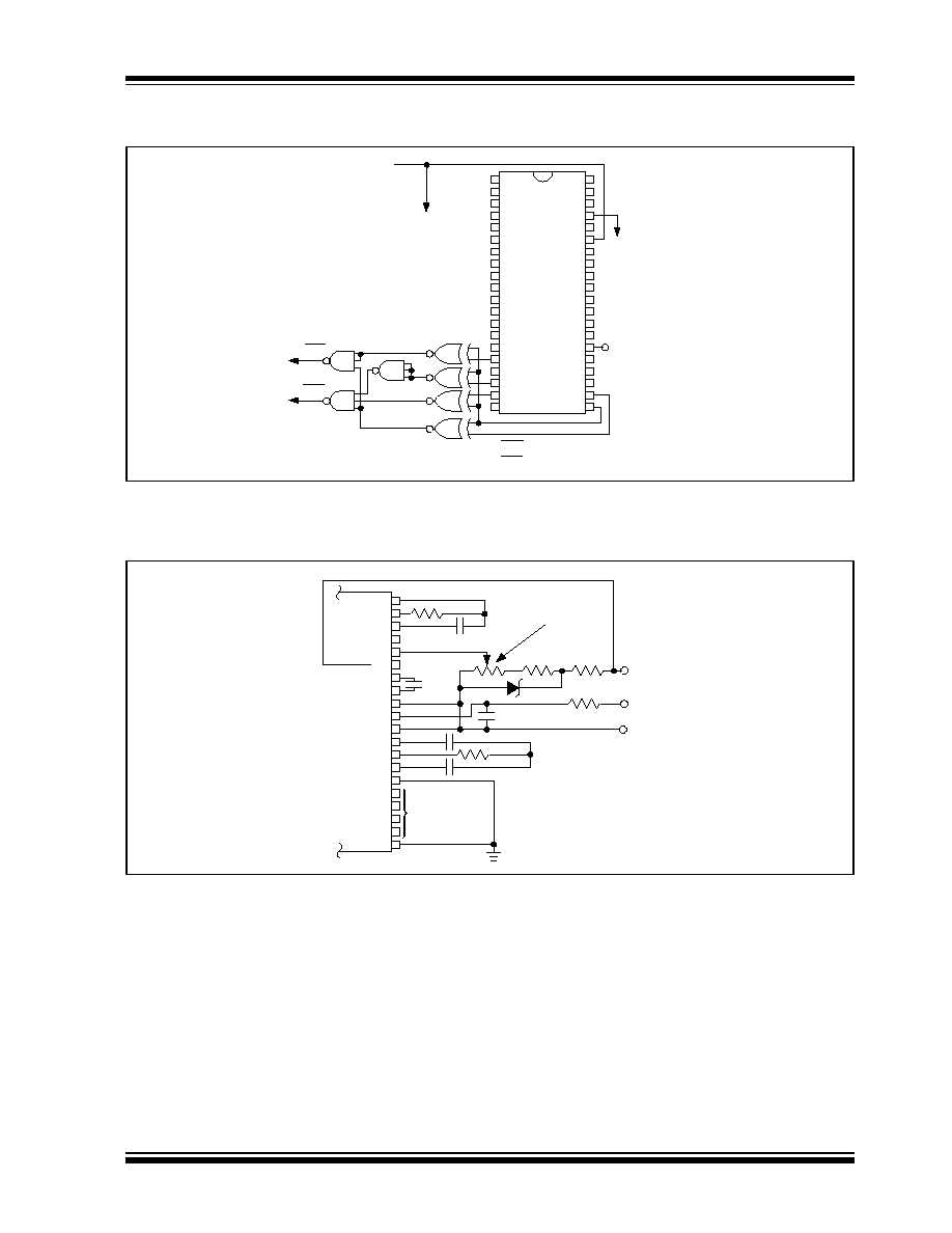
TC7116/TC7117A USING THE INTERNAL REFERENCE
(200mV FULL SCALE, 3 READINGS PER SECOND - RPS)
FIGURE 6-4:
TC7117/TC7117A INTERNAL REFERENCE
(200mV FULL SCALE, 3 RPS, V
IN
- TIED TO GND FOR SINGLE ENDED INPUTS)
100k
100pF
0.47
µF
47k
0.22
µF
To Display
To Backplane
0.1pF
21
1k
22k
9V
Set V
REF
= 100mV
TC7116
TC7116A
0.01
µF
+
In
1M
22
23
24
25
26
27
28
29
30
31
32
33
34
35
36
37
38
39
40
+
100k
100pF
0.47
µF
47k
0.22
µF
To Display
0.1pF
21
1k
22k
Set V
REF
= 100mV
0.01
µF
+
In
1M
22
23
24
25
26
27
28
29
30
31
32
33
34
35
36
37
38
39
40
-5V
+5V
TC7117
TC7117A
©
2002 Microchip Technology Inc.
DS21457B-page 15
TC7116/A/TC7117/A
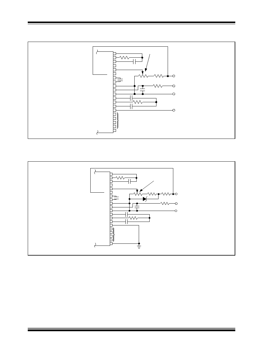
FIGURE 6-5:
CIRCUIT FOR DEVELOPING UNDER RANGE AND OVER RANGE SIGNALS
FROM TC7116/TC7117A OUTPUTS
FIGURE 6-6:
TC7117/TC7117A WITH A 1.2 EXTERNAL BANDGAP REFERENCE
(V
IN
- TIED TO COMMON)
21
20
40
35
26
To Logic
GND
V-
To Logic V
CC
V+
CD4077
U/R
O/R
CD4023
or 74C10
TC7116
TC7116A
O/R = Over Range
U/R = Under Range
100pF
0.47
µF
47k
To Display
0.1pF
1k
V+
Set V
REF
= 100mV
10k
10k
1.2V
0.01
µF
In
1M
+
100k
0.22
µF
21
22
23
24
25
26
27
28
29
30
31
32
33
34
35
36
37
38
39
40
TC7117
TC7117A
TC7116/A/TC7117/A
DS21457B-page 16
©
2002 Microchip Technology Inc.
FIGURE 6-7:
RECOMMENDED COMPONENT VALUES FOR 2V FULL SCALE
(TC7116/TC7116A AND TC7117/TC7117A)
FIGURE 6-8:
TC7117/TC7117A OPERATED FROM SINGLE +5V SUPPLY
(AN EXTERNAL REFERENCE MUST BE USED IN THIS APPLICATION)
100k
100pF
0.047
µF
470k
0.22
µF
To Display
0.1
µF
25k
24k
V+
Set V
REF
= 1V
0.01
µF
+
In
1M
V-
21
22
23
24
25
26
27
28
29
30
31
32
33
34
35
36
37
38
39
40
TC7116
TC7116A
TC7117
TC7117A
100pF
0.47
µF
47k
To Display
0.1pF
1k
V+
Set V
REF
= 100mV
10k
10k
1.2V
0.01
µF
In
1M
+
100k
0.22
µF
21
22
23
24
25
26
27
28
29
30
31
32
33
34
35
36
37
38
39
40
TC7117
TC7117A
©
2002 Microchip Technology Inc.
DS21457B-page 17
TC7116/A/TC7117/A
7.0
PACKAGING INFORMATION
7.1
Package Marking Information
Package marking data not available at this time.
7.2
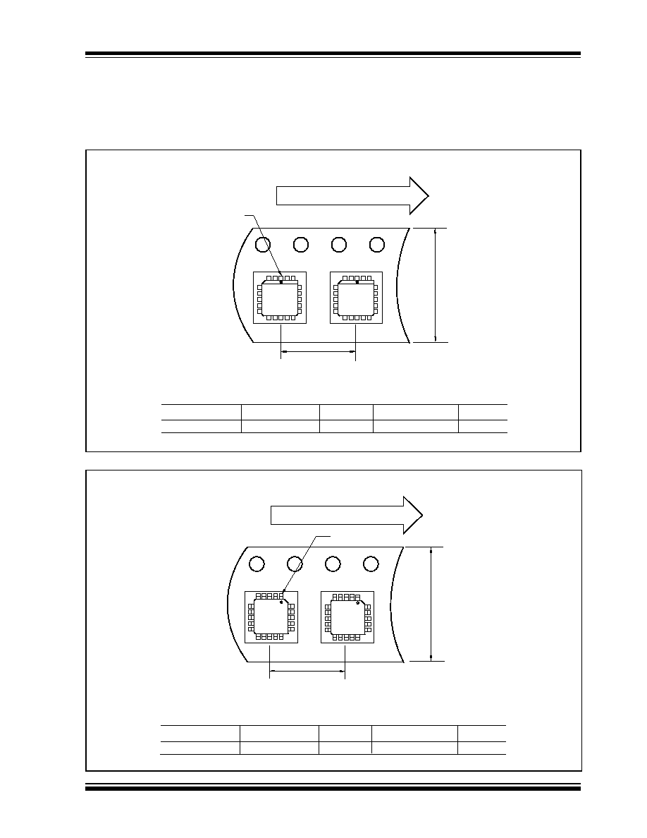
Taping Form
PIN 1
Component Taping Orientation for 44-Pin PLCC Devices
User Direction of Feed
Standard Reel Component Orientation
for TR Suffix Device
Note: Drawing does not represent total number of pins.
W
P
Package
Carrier Width (W)
Pitch (P)
Part Per Full Reel
Reel Size
44-Pin PLCC
32 mm
24 mm
500
13 in
Carrier Tape, Number of Components Per Reel and Reel Size
Component Taping Orientation for 44-Pin PQFP Devices
User Direction of Feed
PIN 1
Standard Reel Component Orientation
for TR Suffix Device
W
P
Package
Carrier Width (W)
Pitch (P)
Part Per Full Reel
Reel Size
44-Pin PQFP
24 mm
16 mm
500
13 in
Carrier Tape, Number of Components Per Reel and Reel Size
Note: Drawing does not represent total number of pins.
TC7116/A/TC7117/A
DS21457B-page 18
©
2002 Microchip Technology Inc.
7.3
Package Dimensions
Dimensions: inches (mm)
2.065 (52.45)
2.027 (51.49)
.200 (5.08)
.140 (3.56)
.150 (3.81)
.115 (2.92)
.070 (1.78)
.045 (1.14)
.022 (0.56)
.015 (0.38)
.110 (2.79)
.090 (2.29)
.555 (14.10)
.530 (13.46)
.610 (15.49)
.590 (14.99)
.015 (0.38)
.008 (0.20)
.700 (17.78)
.610 (15.50)
.040 (1.02)
.020 (0.51)
40-Pin PDIP (Wide)
PIN 1
3
° MIN.
Dimensions: inches (mm)
.015 (0.38)
.008 (0.20)
.620 (15.75)
.590 (15.00)
.700 (17.78)
.620 (15.75)
.540 (13.72)
.510 (12.95)
2.070 (52.58)
2.030 (51.56)
.210 (5.33)
.170 (4.32)
.020 (0.51)
.016 (0.41)
.110 (2.79)
.090 (2.29)
.065 (1.65)
.045 (1.14)
.200 (5.08)
.125 (3.18)
.098 (2.49) MAX.
.030 (0.76) MIN.
.060 (1.52)
.020 (0.51)
.150 (3.81)
MIN.
40-Pin CERDIP (Wide)
PIN 1
3
° MIN.
©
2002 Microchip Technology Inc.
DS21457B-page 19
TC7116/A/TC7117/A
7.3
Package Dimensions (Continued)
Dimenisons: inches (mm)
.695 (17.65)
.685 (17.40)
.656 (16.66)
.650 (16.51)
.656 (16.66)
.650 (16.51)
.021 (0.53)
.013 (0.33)
.032 (0.81)
.026 (0.66)
.630 (16.00)
.591 (15.00)
.120 (3.05)
.090 (2.29)
.180 (4.57)
.165 (4.19)
.695 (17.65)
.685 (17.40)
.050 (1.27) TYP.
.020 (0.51) MIN.
PIN 1
44-Pin PLCC
Dimenisons: inches (mm)
.557 (14.15)
.537 (13.65)
.398 (10.10)
.390 (9.90)
.031 (0.80) TYP.
.018 (0.45)
.012 (0.30)
.398 (10.10)
.390 (9.90)
.010 (0.25) TYP.
.096 (2.45) MAX.
.557 (14.15)
.537 (13.65)
.083 (2.10)
.075 (1.90)
.041 (1.03)
.026 (0.65)
7
° MAX.
.009 (0.23)
.005 (0.13)
44-Pin PQFP
PIN 1
TC7116/A/TC7117/A
DS21457B-page 20
©
2002 Microchip Technology Inc.
PRODUCT IDENTIFICATION SYSTEM
To order or obtain information, e.g., on pricing or delivery, refer to the factory or the listed sales office.
SALES AND SUPPORT
Data Sheets
Products supported by a preliminary Data Sheet may have an errata sheet describing minor operational differences and recom-
mended workarounds. To determine if an errata sheet exists for a particular device, please contact one of the following:
1.
Your local Microchip sales office
2.
The Microchip Corporate Literature Center U.S. FAX: (480) 792-7277
3.
The Microchip Worldwide Site (www.microchip.com)
Please specify which device, revision of silicon and Data Sheet (include Literature #) you are using.
New Customer Notification System
Register on our web site (www.microchip.com/cn) to receive the most current information on our products.
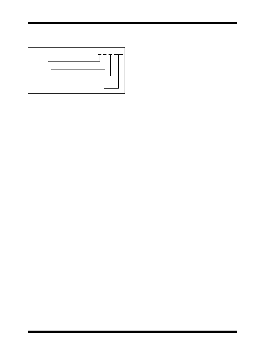
PART CODE
TC711X X X XXX
6 = LCD
7 = LED
A or blank*
R (reversed pins) or blank (CPL pkg only)
* "A" parts have an improved reference TC
Package Code (see Device Selection Table)
}
©
2002 Microchip Technology Inc.
DS21457B-page 21
TC7116/ATC7117/A
Information contained in this publication regarding device
applications and the like is intended through suggestion only
and may be superseded by updates. It is your responsibility to
ensure that your application meets with your specifications.
No representation or warranty is given and no liability is
assumed by Microchip Technology Incorporated with respect
to the accuracy or use of such information, or infringement of
patents or other intellectual property rights arising from such
use or otherwise. Use of Microchip's products as critical com-
ponents in life support systems is not authorized except with
express written approval by Microchip. No licenses are con-
veyed, implicitly or otherwise, under any intellectual property
rights.
Trademarks
The Microchip name and logo, the Microchip logo, FilterLab,
K
EE
L
OQ
, microID,
MPLAB, PIC, PICmicro, PICMASTER,
PICSTART, PRO MATE, SEEVAL and The Embedded Control
Solutions Company are registered trademarks of Microchip Tech-
nology Incorporated in the U.S.A. and other countries.
dsPIC, ECONOMONITOR, FanSense, FlexROM, fuzzyLAB,
In-Circuit Serial Programming, ICSP, ICEPIC, microPort,
Migratable Memory, MPASM, MPLIB, MPLINK, MPSIM,
MXDEV, PICC, PICDEM, PICDEM.net, rfPIC, Select Mode
and Total Endurance are trademarks of Microchip Technology
Incorporated in the U.S.A.
Serialized Quick Turn Programming (SQTP) is a service mark
of Microchip Technology Incorporated in the U.S.A.
All other trademarks mentioned herein are property of their
respective companies.
© 2002, Microchip Technology Incorporated, Printed in the
U.S.A., All Rights Reserved.
Printed on recycled paper.
Microchip received QS-9000 quality system
certification for its worldwide headquarters,
design and wafer fabrication facilities in
Chandler and Tempe, Arizona in July 1999
and Mountain View, California in March 2002.
The Company's quality system processes and
procedures are QS-9000 compliant for its
PICmicro
®
8-bit MCUs, K
EE
L
OQ
®
code hopping
devices, Serial EEPROMs, microperipherals,
non-volatile memory and analog products. In
addition, Microchip's quality system for the
design and manufacture of development
systems is ISO 9001 certified.

DS21457B-page 22
©
2002 Microchip Technology Inc.
AMERICAS
Corporate Office
2355 West Chandler Blvd.
Chandler, AZ 85224-6199
Tel: 480-792-7200 Fax: 480-792-7277
Technical Support: 480-792-7627
Web Address: http://www.microchip.com
Rocky Mountain
2355 West Chandler Blvd.
Chandler, AZ 85224-6199
Tel: 480-792-7966 Fax: 480-792-7456
Atlanta
500 Sugar Mill Road, Suite 200B
Atlanta, GA 30350
Tel: 770-640-0034 Fax: 770-640-0307
Boston
2 Lan Drive, Suite 120
Westford, MA 01886
Tel: 978-692-3848 Fax: 978-692-3821
Chicago
333 Pierce Road, Suite 180
Itasca, IL 60143
Tel: 630-285-0071 Fax: 630-285-0075
Dallas
4570 Westgrove Drive, Suite 160
Addison, TX 75001
Tel: 972-818-7423 Fax: 972-818-2924
Detroit
Tri-Atria Office Building
32255 Northwestern Highway, Suite 190
Farmington Hills, MI 48334
Tel: 248-538-2250 Fax: 248-538-2260
Kokomo
2767 S. Albright Road
Kokomo, Indiana 46902
Tel: 765-864-8360 Fax: 765-864-8387
Los Angeles
18201 Von Karman, Suite 1090
Irvine, CA 92612
Tel: 949-263-1888 Fax: 949-263-1338
New York
150 Motor Parkway, Suite 202
Hauppauge, NY 11788
Tel: 631-273-5305 Fax: 631-273-5335
San Jose
Microchip Technology Inc.
2107 North First Street, Suite 590
San Jose, CA 95131
Tel: 408-436-7950 Fax: 408-436-7955
Toronto
6285 Northam Drive, Suite 108
Mississauga, Ontario L4V 1X5, Canada
Tel: 905-673-0699 Fax: 905-673-6509
ASIA/PACIFIC
Australia
Microchip Technology Australia Pty Ltd
Suite 22, 41 Rawson Street
Epping 2121, NSW
Australia
Tel: 61-2-9868-6733 Fax: 61-2-9868-6755
China - Beijing
Microchip Technology Consulting (Shanghai)
Co., Ltd., Beijing Liaison Office
Unit 915
Bei Hai Wan Tai Bldg.
No. 6 Chaoyangmen Beidajie
Beijing, 100027, No. China
Tel: 86-10-85282100 Fax: 86-10-85282104
China - Chengdu
Microchip Technology Consulting (Shanghai)
Co., Ltd., Chengdu Liaison Office
Rm. 2401, 24th Floor,
Ming Xing Financial Tower
No. 88 TIDU Street
Chengdu 610016, China
Tel: 86-28-6766200 Fax: 86-28-6766599
China - Fuzhou
Microchip Technology Consulting (Shanghai)
Co., Ltd., Fuzhou Liaison Office
Unit 28F, World Trade Plaza
No. 71 Wusi Road
Fuzhou 350001, China
Tel: 86-591-7503506 Fax: 86-591-7503521
China - Shanghai
Microchip Technology Consulting (Shanghai)
Co., Ltd.
Room 701, Bldg. B
Far East International Plaza
No. 317 Xian Xia Road
Shanghai, 200051
Tel: 86-21-6275-5700 Fax: 86-21-6275-5060
China - Shenzhen
Microchip Technology Consulting (Shanghai)
Co., Ltd., Shenzhen Liaison Office
Rm. 1315, 13/F, Shenzhen Kerry Centre,
Renminnan Lu
Shenzhen 518001, China
Tel: 86-755-2350361 Fax: 86-755-2366086
Hong Kong
Microchip Technology Hongkong Ltd.
Unit 901-6, Tower 2, Metroplaza
223 Hing Fong Road
Kwai Fong, N.T., Hong Kong
Tel: 852-2401-1200 Fax: 852-2401-3431
India
Microchip Technology Inc.
India Liaison Office
Divyasree Chambers
1 Floor, Wing A (A3/A4)
No. 11, O'Shaugnessey Road
Bangalore, 560 025, India
Tel: 91-80-2290061 Fax: 91-80-2290062
Japan
Microchip Technology Japan K.K.
Benex S-1 6F
3-18-20, Shinyokohama
Kohoku-Ku, Yokohama-shi
Kanagawa, 222-0033, Japan
Tel: 81-45-471- 6166 Fax: 81-45-471-6122
Korea
Microchip Technology Korea
168-1, Youngbo Bldg. 3 Floor
Samsung-Dong, Kangnam-Ku
Seoul, Korea 135-882
Tel: 82-2-554-7200 Fax: 82-2-558-5934
Singapore
Microchip Technology Singapore Pte Ltd.
200 Middle Road
#07-02 Prime Centre
Singapore, 188980
Tel: 65-6334-8870 Fax: 65-6334-8850
Taiwan
Microchip Technology Taiwan
11F-3, No. 207
Tung Hua North Road
Taipei, 105, Taiwan
Tel: 886-2-2717-7175 Fax: 886-2-2545-0139
EUROPE
Denmark
Microchip Technology Nordic ApS
Regus Business Centre
Lautrup hoj 1-3
Ballerup DK-2750 Denmark
Tel: 45 4420 9895 Fax: 45 4420 9910
France
Microchip Technology SARL
Parc d'Activite du Moulin de Massy
43 Rue du Saule Trapu
Batiment A - ler Etage
91300 Massy, France
Tel: 33-1-69-53-63-20 Fax: 33-1-69-30-90-79
Germany
Microchip Technology GmbH
Gustav-Heinemann Ring 125
D-81739 Munich, Germany
Tel: 49-89-627-144 0 Fax: 49-89-627-144-44
Italy
Microchip Technology SRL
Centro Direzionale Colleoni
Palazzo Taurus 1 V. Le Colleoni 1
20041 Agrate Brianza
Milan, Italy
Tel: 39-039-65791-1 Fax: 39-039-6899883
United Kingdom
Arizona Microchip Technology Ltd.
505 Eskdale Road
Winnersh Triangle
Wokingham
Berkshire, England RG41 5TU
Tel: 44 118 921 5869 Fax: 44-118 921-5820
03/01/02
*DS21457B*
W
ORLDWIDE
S
ALES
AND
S
ERVICE