 | ÐлекÑÑоннÑй компоненÑ: TC7129CKW | СкаÑаÑÑ:  PDF PDF  ZIP ZIP |
Äîêóìåíòàöèÿ è îïèñàíèÿ www.docs.chipfind.ru
©
2002 Microchip Technology Inc.
DS21459B-page 1
TC7129
Features
· Count Resolution: ±19,999
· Resolution on 200mV Scale: 10
µ
V
· True Differential Input and Reference
· Low Power Consumption: 500
µ
A at 9V
· Direct LCD Driver for 4-1/2 Digits, Decimal Points,
Low Battery Indicator, and Continuity Indicator
· Over Range and Under Range Outputs
· Range Select Input: 10:1
· High Common Mode Rejection Ratio: 110dB
· External Phase Compensation Not Required
Applications
· Full Featured Multimeters
· Digital Measurement Devices
Device Selection Table
General Description
The TC7129 is a 4-1/2 digit analog-to-digital converter
(ADC) that directly drives a multiplexed liquid crystal
display (LCD). Fabricated in high performance, low
power CMOS, the TC7129 ADC is designed specifi-
cally for high resolution, battery powered digital multi-
meter applications. The traditional dual slope method
of A/D conversion has been enhanced with a succes-
sive integration technique to produce readings accu-
rate to better than 0.005% of full scale, and resolution
down to 10
µ
V per count.
The TC7129 includes features important to multimeter
applications. It detects and indicates low battery condi-
tion. A continuity output drives an annunciator on the
display, and can be used with an external driver to
sound an audible alarm. Over range and under range
outputs and a range change input provide the ability to
create auto-ranging instruments. For snapshot read-
ings, the TC7129 includes a latch-and-hold input to
freeze the present reading. This combination of features
makes the TC7129 the ideal choice for full featured
multimeter and digital measurement applications.
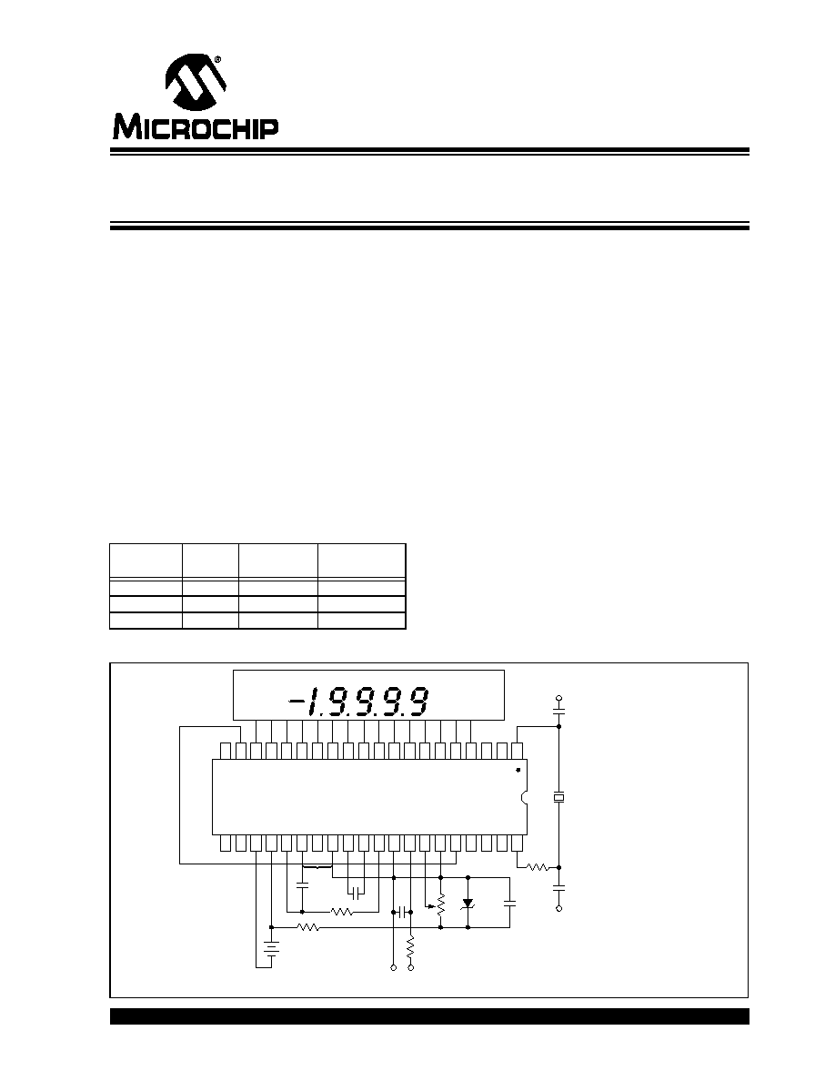
Typical Application
Package
Code
Pin
Layout
Package
Temperature
Range
TC7129CPL
Normal
40-Pin PDIP
0
°
C to +70
°
C
TC7129CKW
Formed
44-Pin PQFP
0
°
C to +70
°
C
TC7129CLW
44-Pin PLCC
0
°
C to +70
°
C
TC7129
1
2
3
4
5
6
7
8
9
10
11
12
13
14
15
16
17
18
19
20
40
39
38
37
36
35
34
33
32
31
30
29
28
27
26
25
24
23
22
21
9V
+
+
Low Battery
Continuity
V+
5pF
120kHz
10pF
0.1
µF
20
k
0.1
µF
100k
1
µF
0.1
µF
150k
10k
V+
V
IN
+
*
*Note: RC network between Pins 26 and 28 is not required.
330k
4-1/2 Digit Analog-to-Digital Converters with
On-Chip LCD Drivers
TC7129
DS21459B-page 2
©
2002 Microchip Technology Inc.
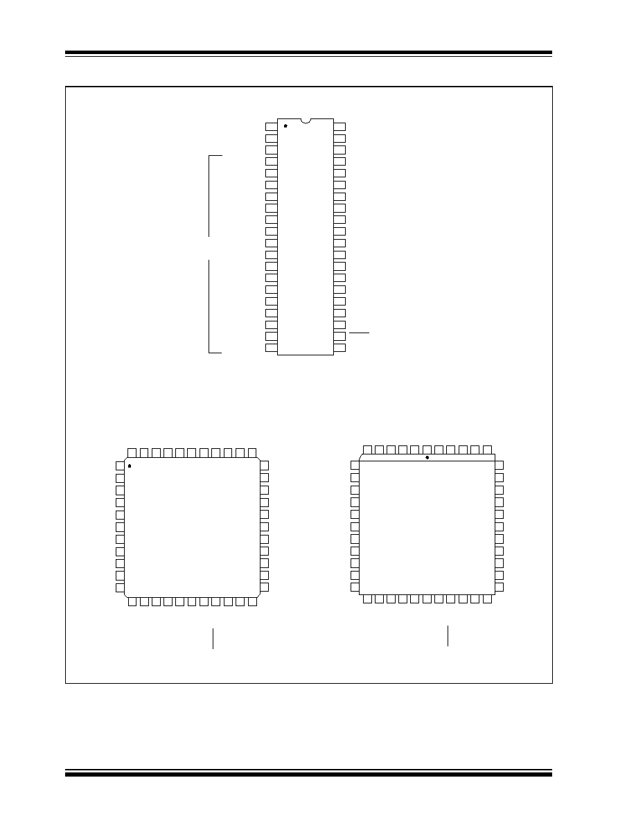
Package Type
33
34
35
36
37
38
39
13
10
9
8
7
18 19 20 21
23 24
6
5
4
3
1
44
2
22
43 42 41 40
25 26 27 28
32
14
31
15
30
16
29
17
11
12
TC7129CLW
F
1
, E
1
, DP
1
B
2
, C
2
, BATT
A
2
, G
2
, D
2
F
2
, E
2
, DP
2
B
3
, C
3
, MINUS
A
3
, G
3
, D
3
F
3
, E
3
, DP
3
B
4
, C
4
, BC
5
A
4
, G
4
, D
4
F
4
, E
4
, DP
4
NC
REF LO
REF HI
IN HI
IN LO
BUFF
C
REF
-
C
REF
+
COMMON
CONTINUITY
INT OUT
NC
A
1
, G
1
, D
1
B
1
, C
1
, CONT
ANNUNCIATOR
OSC3
OSC1
NC
OSC2
DP
1
DP
2
RANGE
DGND
BP
3
BP
2
BP
1
V
DISP
DP
4
/OR
NC
DP
3
/UR
LATCH/HOLD
V+
V-
INT IN
27
28
29
30
31
32
33
7
4
3
2
1
TC7129CKW
12 13 14 15
17 18
44 43 42 41
39 38
40
16
37 36 35 34
19 20 21 22
26
8
25
9
24
10
23
11
5
6
A
1
, G
1
, D
1
B
1
, C
1
, CONT
ANNUNCIATOR
OSC3
OSC1
NC
OSC2
DP
1
DP
2
RANGE
DGND
REF LO
REF HI
IN HI
IN LO
BUFF
C
REF
-
C
REF
+
COMMON
CONTINUITY
INT OUT
NC
F
1
, E
1
, DP
1
B
2
, C
2
, BATT
A
2
, G
2
, D
2
F
2
, E
2
, DP
2
B
3
, C
3
, MINUS
A
3
, G
3
, D
3
F
3
, E
3
, DP
3
B
4
, C
4
, BC
5
A
4
, G
4
, D
4
F
4
, E
4
, DP
4
NC
BP
3
BP
2
BP
1
V
DISP
DP
4
/OR
NC
DP
3
/UR
LATCH/HOLD
V+
V-
INT IN
TC7129CPL
40-Pin PDIP
44-Pin QFP
44-Pin PLCC
1
2
3
4
5
6
7
8
9
10
11
12
13
14
15
16
17
18
19
20
40
39
38
37
36
35
34
33
32
31
30
29
28
27
26
25
24
23
22
21
OSC2
DP
1
DP
2
RANGE
DGND
REF LO
REF HI
IN HI
IN LO
BUFF
C
REF
-
C
REF
+
COMMON
CONTINUITY
INT OUT
INT IN
V+
V-
DP
3
/UR
OSC1
OSC3
ANNUNICATOR
B
1
, C
1
, CONT
A
1
, G
1
, D
1
F
1
, E
1
, DP
1
B
2
, C
2
, LO BATT
A
2
, G
2
, D
2
F
2
, E
2
, DP
2
B
3
, C
3
, MINUS
A
3
, G
3
, D
3
F
3
, E
3
, DP
3
B
4
, C
4
, BC
5
A
4
, G
4
, D
4
F
4
, E
4
, DP
4
BP
3
BP
2
BP
1
V
DISP
DP
4
/OR
Display
Output
Lines
LATCH/HOLD
©
2002 Microchip Technology Inc.
DS21459B-page 3
TC7129
1.0
ELECTRICAL
CHARACTERISTICS
Absolute Maximum Ratings*
Supply Voltage (V+ to V-) ....................................... 15V
Reference Voltage (REF HI or REF LO) ......... V+ to V-
Input Voltage (IN HI or IN LO) (Note 1)........... V+ to V-
V
DISP
.......................................... V+ to (DGND 0.3V)
Digital Input (Pins 1, 2, 19, 20,
21, 22, 27, 37, 39, 40) .......................... DGND to V+
Analog Input (Pins 25, 29, 30) ........................ V+ to V-
Package Power Dissipation (T
A
70°C)
Plastic DIP ..................................................... 1.23W
PLCC ............................................................. 1.23W
Plastic QFP .................................................... 1.00W
Operating Temperature Range ............... 0°C to +70°C
Storage Temperature Range .............. -65°C to +150°C
*Stresses above those listed under "Absolute Maximum
Ratings" may cause permanent damage to the device. These
are stress ratings only and functional operation of the device
at these or any other conditions above those indicated in the
operation sections of the specifications is not implied.
Exposure to Absolute Maximum Rating conditions for
extended periods may affect device reliability.
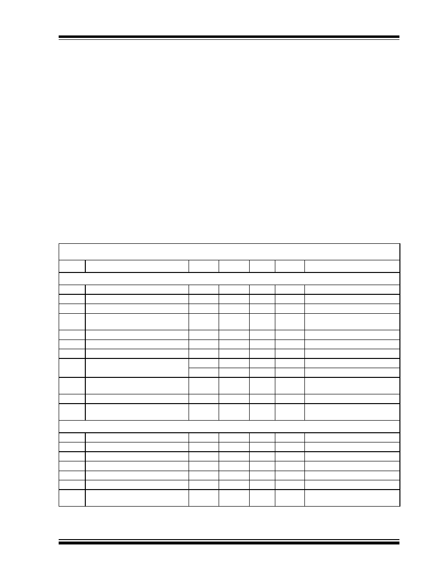
TC7129 ELECTRICAL SPECIFICATIONS
Electrical Characteristics: V+ to V- = 9V, V
REF
= 1V, T
A
= +25°C, f
CLK
= 120kHz, unless otherwise indicated.
Pin numbers refer to 40-pin DIP.
Symbol
Parameter
Min
Typ
Max
Unit
Test Conditions
Input
Zero Input Reading
-0000
0000
+0000
Counts
V
IN
= 0V, 200mV Scale
Zero Reading Drift
--
±0.5
--
µ
V/°C
V
IN
= 0V, 0°C < T
A
< +70°C
Ratiometric Reading
9997
9999
10000
Counts
V
IN
= V
REF
= 1000mV, Range = 2V
Range Change Accuracy
0.9999
1.0000
1.0001
Ratio
V
IN
= 1V on High Range,
V
IN
= 0.1V on Low Range
RE
Rollover Error
--
1
2
Counts
V
IN
- = V
IN
+ = 199mV
NL
Linearity Error
--
1
--
Counts
200mV Scale
CMRR
Common Mode Rejection Ratio
--
110
--
dB
V
CM
= 1V, V
IN
= 0V, 200mV Scale
CMVR
Common Mode Voltage Range
--
(V-) + 1.5
--
V
V
IN
= 0V
--
(V+) 1
--
V
200mV Scale
e
N
Noise (Peak-to-Peak Value not
Exceeded 95% of Time)
--
14
--
µ
V
P-P
V
IN
= 0V
200mV Scale
I
IN
Input Leakage Current
--
1
10
pA
V
IN
= 0V, Pins 32, 33
Scale Factor Temperature Coefficient
--
2
7
ppm/°C
V
IN
= 199mV, 0°C < T
A
< +70°C
External V
REF
= 0ppm/°C
Power
V
COM
Common Voltage
2.8
3.2
3.5
V
V+ to Pin 28
Common Sink Current
--
0.6
--
mA
Common = +0.1V
Common Source Current
--
10
--
µ
A
Common = -0.1V
DGND
Digital Ground Voltage
4.5
5.3
5.8
V
V+ to Pin 36, V+ to V- = 9V
Sink Current
--
1.2
--
mA
DGND = +0.5V
Supply Voltage Range
6
9
12
V
V+ to V-
I
S
Supply Current Excluding Common
Current
--
0.8
1.3
mA
V+ to V- = 9V
Note
1:
Input voltages may exceed supply voltages, provided input current is limited to ±400
µ
A. Currents above this value may
result in invalid display readings, but will not destroy the device if limited to ±1mA. Dissipation ratings assume device is
mounted with all leads soldered to printed circuit board.
TC7129
DS21459B-page 4
©
2002 Microchip Technology Inc.
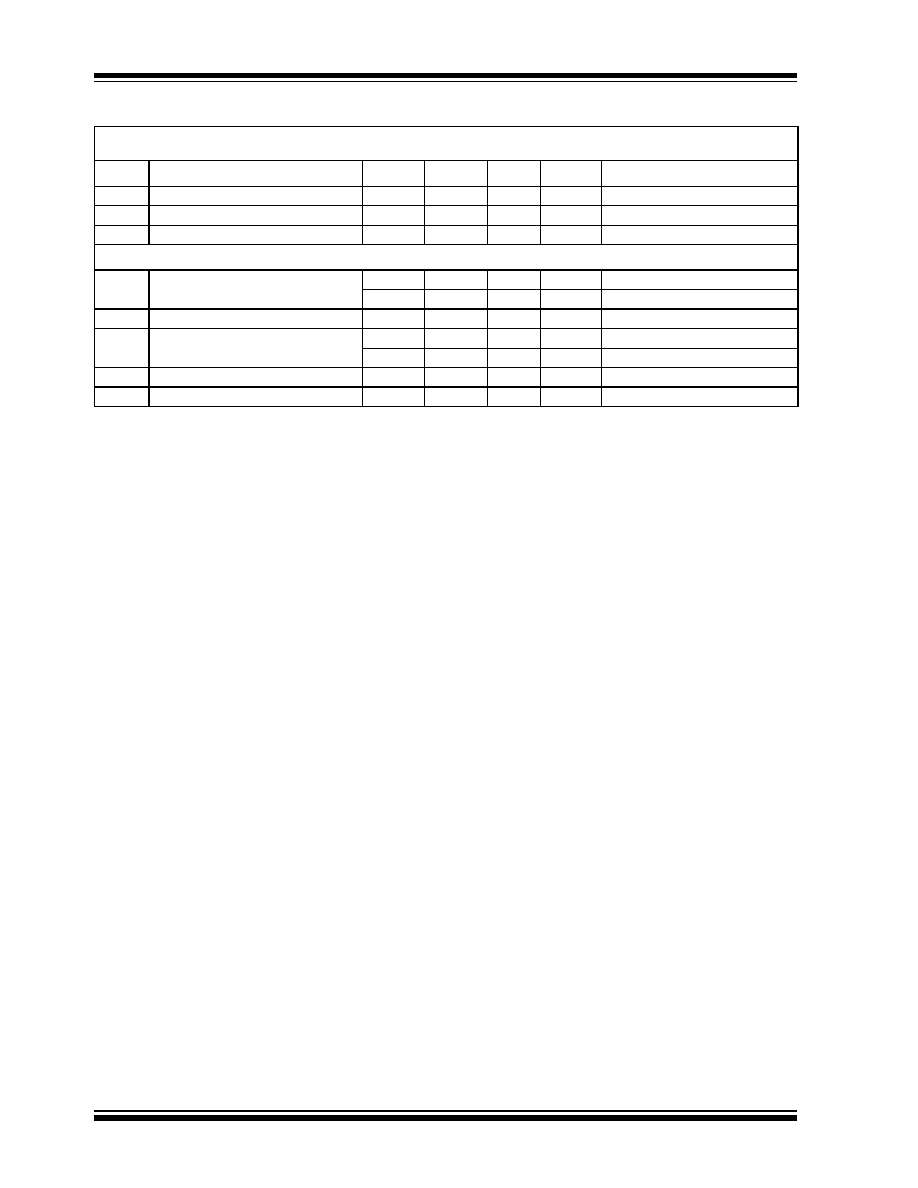
f
CLK
Clock Frequency
--
120
360
kHz
V
DISP
Resistance
--
50
--
k
V
DISP
to V+
Low Battery Flag Activation Voltage
6.3
7.2
7.7
V
V+ to V-
Digital
Continuity Comparator Threshold
Voltages
100
200
--
mV
V
OUT
Pin 27 = High
--
200
400
mV
V
OUT
Pin 27 = Low
Pull-down Current
--
2
10
µ
A
Pins 37, 38, 39
"Weak Output" Current
Sink/Source
--
3/3
--
µ
A
Pins 20, 21 Sink/Source
--
3/9
--
µ
A
Pin 27 Sink/Source
Pin 22 Source Current
--
40
--
µ
A
Pin 22 Sink Current
--
3
--
µ
A
TC7129 ELECTRICAL SPECIFICATIONS (CONTINUED)
Electrical Characteristics: V+ to V- = 9V, V
REF
= 1V, T
A
= +25°C, f
CLK
= 120kHz, unless otherwise indicated.
Pin numbers refer to 40-pin DIP.
Symbol
Parameter
Min
Typ
Max
Unit
Test Conditions
Note
1:
Input voltages may exceed supply voltages, provided input current is limited to ±400
µ
A. Currents above this value may
result in invalid display readings, but will not destroy the device if limited to ±1mA. Dissipation ratings assume device is
mounted with all leads soldered to printed circuit board.
©
2002 Microchip Technology Inc.
DS21459B-page 5
TC7129
2.0
PIN DESCRIPTIONS
The descriptions of the pins are listed in Table 2-1.
TABLE 2-1:
PIN FUNCTION TABLE
Pin No.
40-Pin PDIP
Pin No.
44-Pin PQFP
Pin No.
44-Pin PLCC
Symbol
Function
1
40
2
OSC1
Input to first clock inverter.
2
41
3
OSC3
Output of second clock inverter.
3
42
4
ANNUNCIATOR Backplane square wave output for driving annunciators.
4
43
5
B
1
, C
1
, CONT
Output to display segments.
5
44
6
A
1
, G
1
, D
1
Output to display segments.
6
1
7
F
1
, E
1
, DP
1
Output to display segments.
7
2
8
B
2
, C
2
, LO BATT Output to display segments.
8
3
9
A
2
, G
2
, D
2
Output to display segments.
9
4
10
F
2
, E
2
, DP
2
Output to display segments.
10
5
11
B
3
, C
3
, MINUS
Output to display segments.
11
7
13
A
3
, G
3
, D
3
Output to display segments.
12
8
14
F
3
, E
3
, DP
3
Output to display segments.
13
9
15
B
4
, C
4
, BC
5
Output to display segments.
14
10
16
A
4
, D
4
, G
4
Output to display segments.
15
11
17
F
4
, E
4
, DP
4
Output to display segments.
16
12
18
BP
3
Backplane #3 output to display.
17
13
19
BP
2
Backplane #2 output to display.
18
14
20
BP
1
Backplane #1 output to display.
19
15
21
V
DISP
Negative rail for display drivers.
20
16
22
DP
4
/OR
Input: When HI, turns on most significant decimal point.
Output: Pulled HI when result count exceeds ±19,999.
21
18
24
DP
3
/UR
Input: Second most significant decimal point on when HI.
Output: Pulled HI when result count is less than ±1000.
22
19
25
LATCH/HOLD
Input: When floating, ADC operates in the Free Run mode. When
pulled HI, the last displayed reading is held. When pulled LO, the
result counter contents are shown incrementing during the
de-integrate phase of cycle.
Output: Negative going edge occurs when the data latches are
updated. Can be used for converter status signal.
23
20
26
V-
Negative power supply terminal.
24
21
27
V+
Positive power supply terminal and positive rail for display drivers.
25
22
28
INT IN
Input to integrator amplifier.
26
23
29
INT OUT
Output of integrator amplifier.
27
24
30
CONTINUITY
Input: When LO, continuity flag on the display is OFF. When HI,
continuity flag is ON.
Output: HI when voltage between inputs is less than +200mV. LO
when voltage between inputs is more than +200mV.
28
25
31
COMMON
Sets Common mode voltage of 3.2V below V+ for DE, 10X, etc.
Can be used as pre-regulator for external reference.
29
26
32
C
REF
+
Positive side of external reference capacitor.
30
27
33
C
REF-
Negative side of external reference capacitor.
31
29
35
BUFFER
Output of buffer amplifier.
32
30
36
IN LO
Negative input voltage terminal.
33
31
37
IN HI
Positive input voltage terminal.
34
32
38
REF HI
Positive reference voltage.
35
33
39
REF LO
Negative reference voltage
TC7129
DS21459B-page 6
©
2002 Microchip Technology Inc.
36
34
40
DGND
Internal ground reference for digital section. See Section 4.3,
±5V Power Supply.
37
35
41
RANGE
3
µ
A pull-down for 200mV scale. Pulled HI externally for 2V scale.
38
36
42
DP
2
Internal 3
µ
A pull-down. When HI, decimal point 2 will be on.
39
37
43
DP
1
Internal 3
µ
A pull-down. When HI, decimal point 1 will be on.
40
38
44
OSC2
Output of first clock inverter. Input of second clock inverter.
--
6,17, 28, 39
12, 23, 34, 1
NC
No connection.
TABLE 2-1:
PIN FUNCTION TABLE (CONTINUED)
Pin No.
40-Pin PDIP
Pin No.
44-Pin PQFP
Pin No.
44-Pin PLCC
Symbol
Function
©
2002 Microchip Technology Inc.
DS21459B-page 7
TC7129
3.0
DETAILED DESCRIPTION
(All Pin Designations Refer to 40-Pin PDIP.)
The TC7129 is designed to be the heart of a high
resolution analog measurement instrument. The only
additional components required are a few passive ele-
ments: a voltage reference, an LCD, and a power
source. Most component values are not critical; substi-
tutes can be chosen based on the information given
below.
The basic circuit for a digital multimeter application is
shown in Figure 3-1. See Section 4.0, Typical Applica-
tions for variations. Typical values for each component
are shown. The sections below give component selec-
tion criteria.
3.1
Oscillator (X
OSC
, C
O1
, C
O2
, R
O
)
The primary criterion for selecting the crystal oscillator
is to choose a frequency that achieves maximum rejec-
tion of line frequency noise. To do this, the integration
phase should last an integral number of line cycles.
The integration phase of the TC7129 is 10,000 clock
cycles on the 200mV range and 1000 clock cycles on
the 2V range. One clock cycle is equal to two oscillator
cycles. For 60Hz rejection, the oscillator frequency
should be chosen so that the period of one line cycle
equals the integration time for the 2V range:
EQUATION 3-1:
This equation gives an oscillator frequency of 120kHz.
A similar calculation gives an optimum frequency of
100kHz for 50Hz rejection.
The resistor and capacitor values are not critical; those
shown work for most applications. In some situations,
the capacitor values may have to be adjusted to com-
pensate for parasitic capacitance in the circuit. The
capacitors can be low cost ceramic devices.
Some applications can use a simple RC network
instead of a crystal oscillator. The RC oscillator has
more potential for jitter, especially in the least
significant digit. See Section 4.8, RC Oscillator.
3.2
Integrating Resistor (R
INT
)
The integrating resistor sets the charging current for
the integrating capacitor. Choose a value that provides
a current between 5
µ
A and 20
µ
A at 2V, the maximum
full scale input. The typical value chosen gives a
charging current of 13.3
µ
A:
EQUATION 3-2:
Too high a value for R
INT
increases the sensitivity to
noise pickup and increases errors due to leakage cur-
rent. Too low a value degrades the linearity of the
integration, leading to inaccurate readings.
1/60 second = 16.7msec =
1000 clock cycles *2 OSC cycles/clock cycle
OSC Frequency
I
CHARGE
=
2V
150k
13.3
µ
A
TC7129
DS21459B-page 8
©
2002 Microchip Technology Inc.
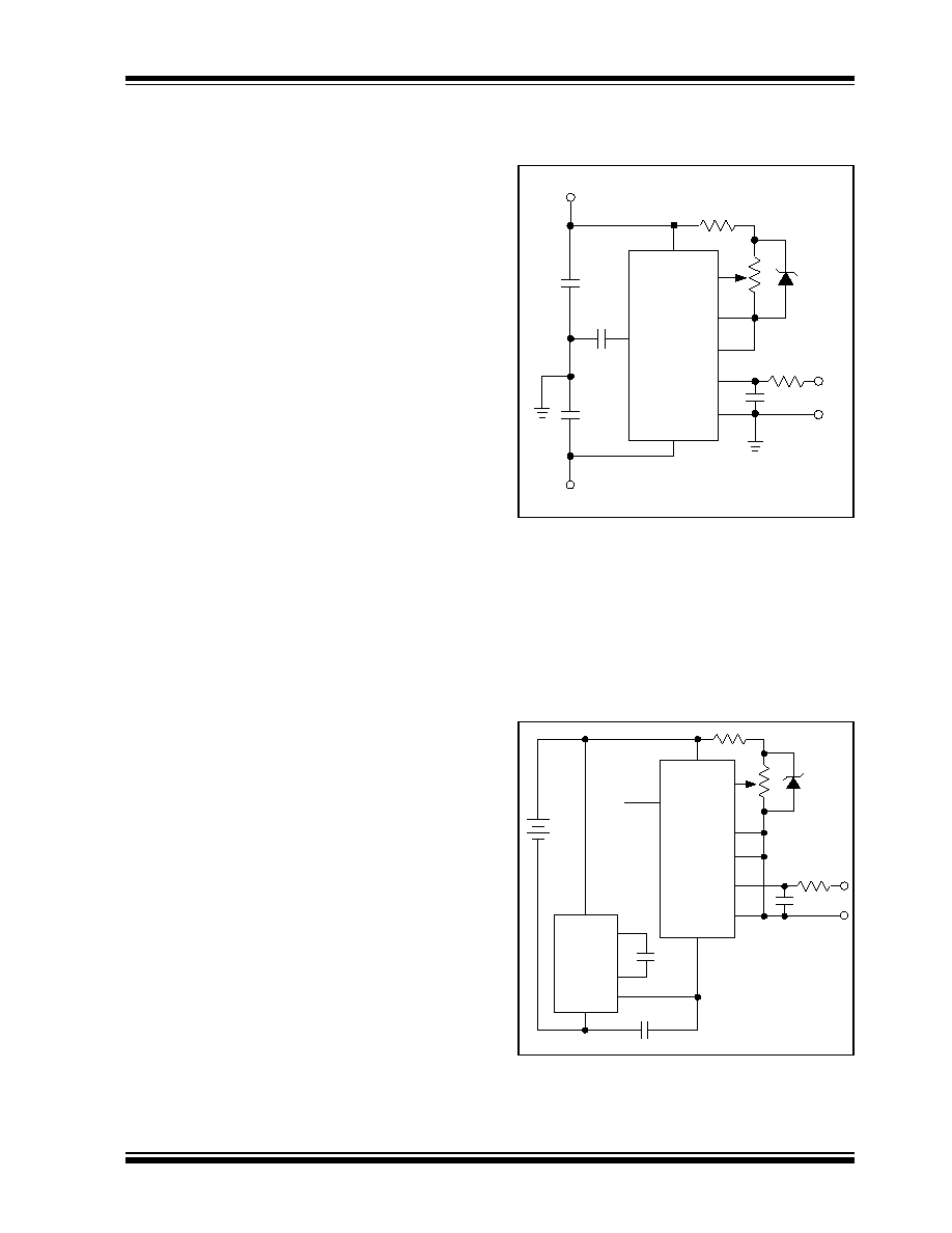
FIGURE 3-1:
STANDARD CIRCUIT
3.3
Integrating Capacitor (C
INT
)
The charge stored in the integrating capacitor during
the integrate phase is directly proportional to the input
voltage. The primary selection criterion for C
INT
is to
choose a value that gives the highest voltage swing
while remaining within the high linearity portion of the
integrator output range. An integrator swing of 2V is the
recommended value. The capacitor value can be
calculated using the following equation:
EQUATION 3-3:
Using the values derived above (assuming 60Hz
operation), the equation becomes:
EQUATION 3-4:
The capacitor should have low dielectric absorption to
ensure good integration linearity. Polypropylene and
Teflon capacitors are usually suitable. A good mea-
surement of the dielectric absorption is to connect the
reference capacitor across the inputs by connecting:
Pin to Pin:
20
33 (C
REF
+ to IN HI)
30
32 (C
REF
- to IN LO)
A reading between 10,000 and 9998 is acceptable;
anything lower indicates unacceptably high dielectric
absorption.
3.4
Reference Capacitor (C
REF
)
The reference capacitor stores the reference voltage
during several phases of the measurement cycle. Low
leakage is the primary selection criterion for this com-
ponent. The value must be high enough to offset the
effect of stray capacitance at the capacitor terminals. A
value of at least 1
µ
F is recommended.
1
2
3
4
5
6
7
8
9
10
11
12
13
14
15
16
17
18
19
20
40
39
38
37
36
35
34
33
32
31
30
29
28
27
26
25
24
23
22
21
9V
+
Low Battery Continuity
V+
5pF
120
kHz
10pF
0.1
µF
20
k
0.1
µF
100k
C
INT
0.1
µF
V+
V
IN
+
330k
Crystal
R
O
C
O2
C
RF
D
REF
R
REF
C
IF
R
IF
C
REF
+
1
µF
10k
R
BIAS
150k
R
INT
OSC1
OSC3
ANNUNC
V
DISP
DP
4
/OR
Display Drive Outputs
DP
3
/UR
LATCH/
HOLD
V-
V+
INT IN
INT OUT
CONTINUITY
COMMON
C
REF
+
C
REF
-
BUFF
IN LO
IN HI
REF HI
REF LO
DGND
RANGE
DP
2
DP
1
OSC2
TC7129
C
O1
C
INT
=
t
INT
x I
INT
V
SWING
Where t
INT
is the integration time.
C
INT
=
= 0.1
µ
A
16.7msec x 13.3
µ
A
2V
©
2002 Microchip Technology Inc.
DS21459B-page 9
TC7129
3.5
Voltage Reference
(D
REF
, R
REF
, R
BIAS
, C
RF
)
The reference potentiometer (R
REF
) provides an
adjustment for adjusting the reference voltage; any
value above 20k
is adequate. The bias resistor
(R
BIAS
) limits the current through D
REF
to less than
150
µ
A. The reference filter capacitor (C
RF
) forms an
RC filter with R
BIAS
to help eliminate noise.
3.6
Input Filter (R
IF
, C
IF
)
For added stability, an RC input noise filter is usually
included in the circuit. The input filter resistor value
should not exceed 100k
. A typical RC time constant
value is 16.7msec to help reject line frequency noise.
The input filter capacitor should have low leakage for a
high-impedance input.
3.7
Battery
The typical circuit uses a 9V battery as a power source.
Any value between 6V and 12V can be used. For oper-
ation from batteries with voltages lower than 6V and for
operation from power supplies, see Section 4.2,
Powering the TC7129.
4.0
TYPICAL APPLICATIONS
4.1
TC7129 as a Replacement Part
The TC7129 is a direct pin-for-pin replacement part for
the ICL7129. Note, however, that part requires a
capacitor and resistor between Pins 26 and 28 for
phase compensation. Since the TC7129 uses internal
phase compensation, these parts are not required and,
in fact, must be removed from the circuit for stable
operation.
4.2
Powering the TC7129
While the most common power source for the TC7129
is a 9V battery, there are other possibilities. Some of
the more common ones are explained below.
4.3
±5V Power Supply
Measurements are made with respect to power supply
ground. DGND (Pin 36) is set internally to about 5V
less than V
+
(Pin 24); it is not intended as a power sup-
ply input and must not be tied directly to power supply
ground. It can be used as a reference for external logic,
as explained in Section 4.6, Connecting to External
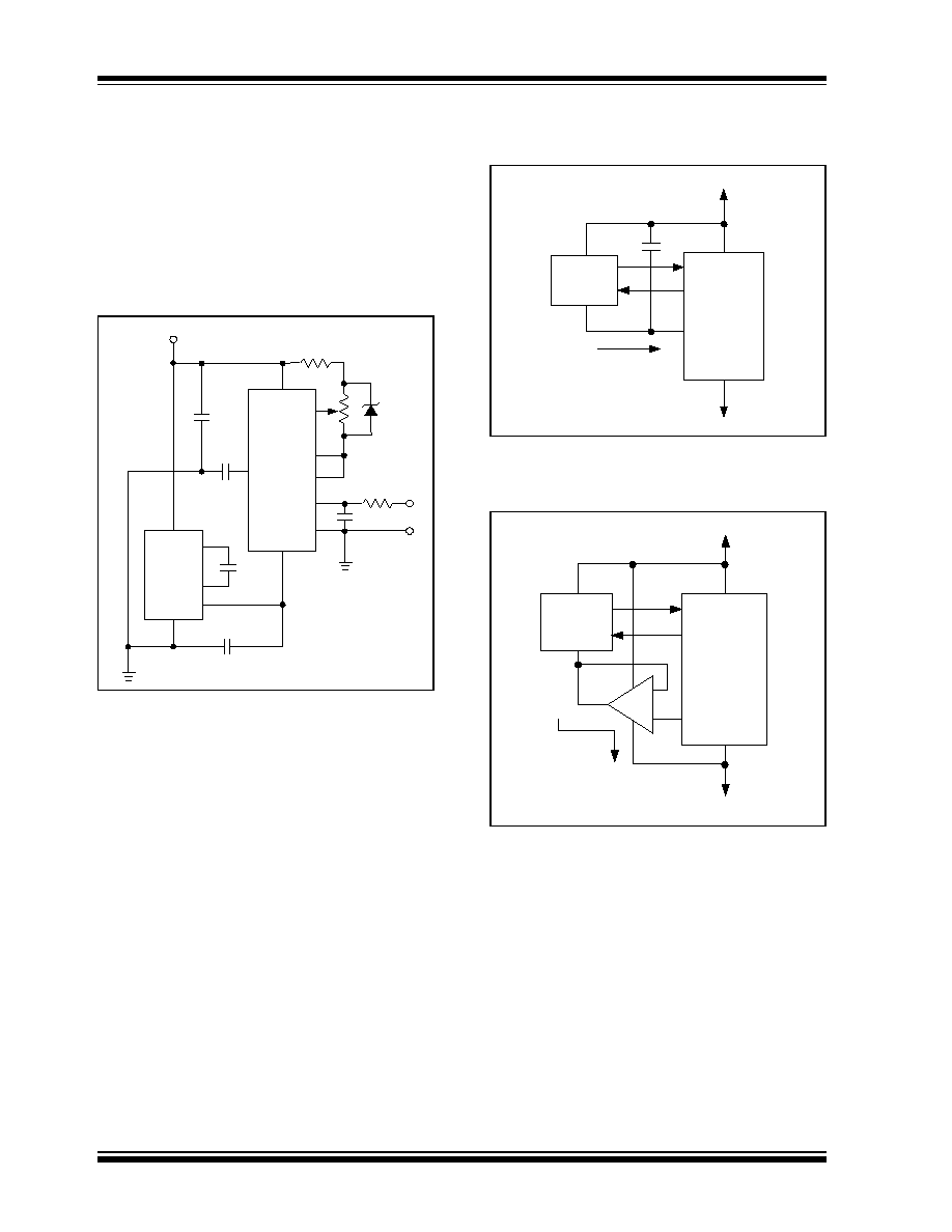
Logic (see Figure 4-1).
FIGURE 4-1:
POWERING THE TC7129
FROM A ±5V POWER
SUPPLY
4.4
Low Voltage Battery Source
A battery with voltage between 3.8V and 6V can be
used to power the TC7129, when used with a voltage
doubler circuit, as shown in Figure 4-2. The voltage
doubler uses the TC7660 DC-to-DC voltage converter
and two external capacitors.
FIGURE 4-2:
POWERING THE TC7129
FROM A LOW VOLTAGE
BATTERY
V-
V+
REF HI
REF LO
IN HI
COMMON
IN LO
DGND
V
IN
+
-5V
0.1
µF
+5V
0.1
µF
24
34
35
28
33
32
23
36
TC7129
0.1
µF
V-
TC7129
V+
REF HI
REF LO
IN HI
COMMON
IN LO
DGND
3.8V
to
6V
+
+
10
µF
+
8
2
4
10
µF
+
3
TC7660
V
IN
5
24
34
35
28
33
32
23
36
TC7129
DS21459B-page 10
©
2002 Microchip Technology Inc.
4.5
+5V Power Supply
Measurements are made with respect to power supply
ground. COMMON (Pin 28) is connected to REF LO
(Pin 35). A voltage doubler is needed, since the supply
voltage is less than the 6V minimum needed by the
TC7129. DGND (Pin 36) must be isolated from power
supply ground (see Figure 4-3).
FIGURE 4-3:
POWERING THE TC7129
FROM A +5V POWER
SUPPLY
4.6
Connecting to External Logic
External logic can be directly referenced to DGND
(Pin 36), provided that the supply current of the exter-
nal logic does not exceed the sink current of DGND
(Figure 4-4). A safe value for DGND sink current is
1.2mA. If the sink current is expected to exceed this
value, a buffer is recommended (see Figure 4-5).
FIGURE 4-4:
EXTERNAL LOGIC
REFERENCED DIRECTLY
TO DGND
FIGURE 4-5:
EXTERNAL LOGIC
REFERENCED TO DGND
WITH BUFFER
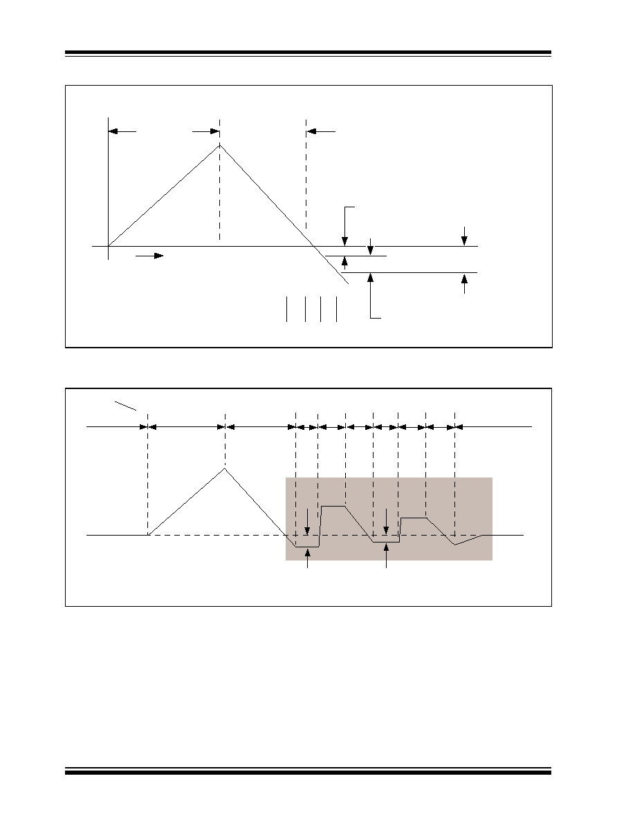
4.7
Temperature Compensation
For most applications, V
DISP
(Pin 19) can be connected
directly to DGND (Pin 36). For applications with a wide
temperature range, some LCDs require that the drive
levels vary with temperature to maintain good viewing
angle and display contrast. Figure 4-6 shows two cir-
cuits that can be adjusted to give temperature com-
pensation of about 10mV/°C between V+ (Pin 24) and
V
DISP
. The diode between DGND and V
DISP
should
have a low turn-on voltage because V
DISP
cannot
exceed 0.3V below DGND.
V-
V+
DGND
+
10
µF
+
8
2
4
10
µF
+
3
V
IN
5
24
34
35
28
33
32
23
36
TC7660
V+
GND
0.1
µF
0.1
µF
+5V
TC7129
External
Logic
DGND
V
+
36
24
23
I
LOGIC
TC7129
V-
+
External
Logic
I
LOGIC
DGND
23
24
V+
36
TC7129
V-
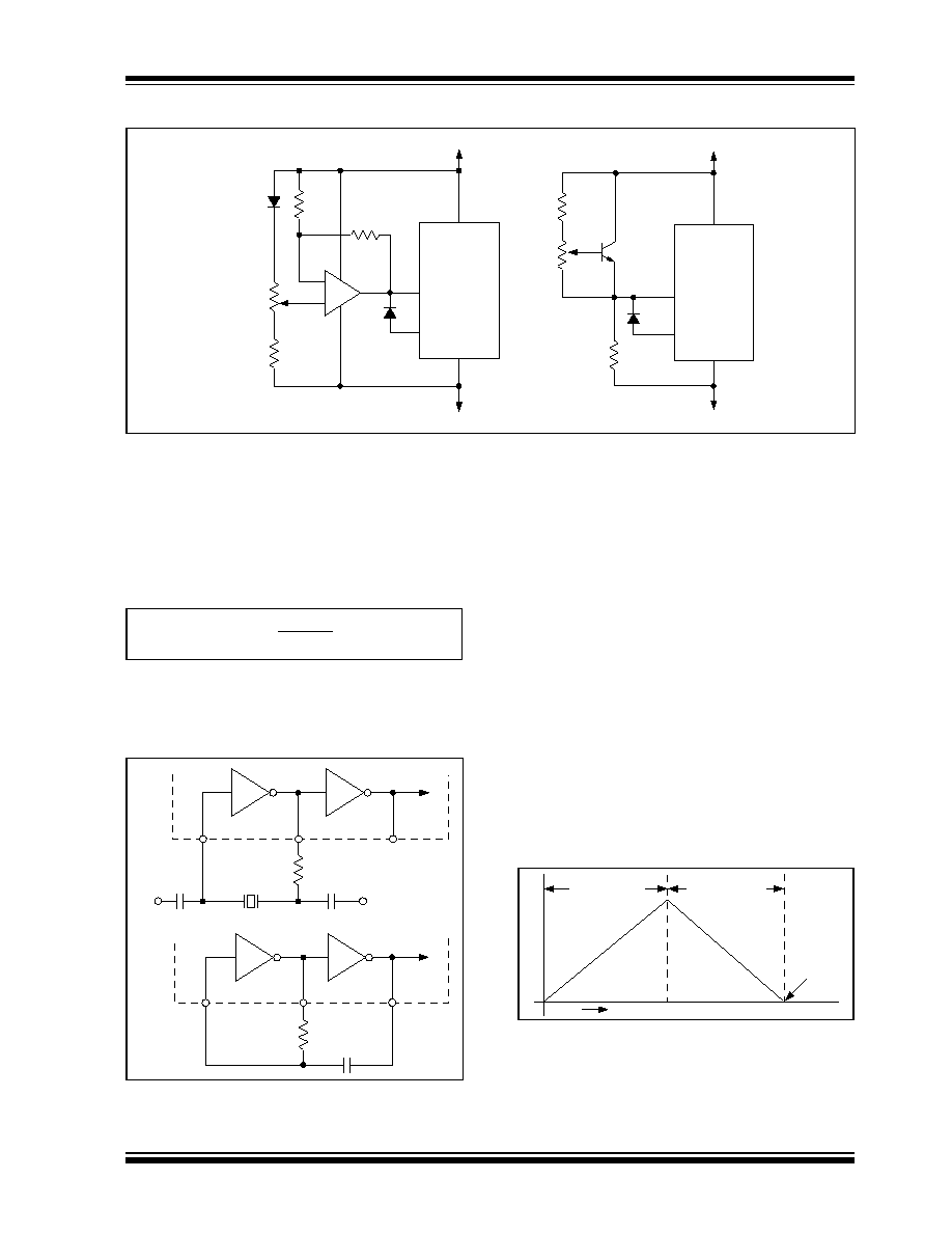
©
2002 Microchip Technology Inc.
DS21459B-page 11
TC7129
FIGURE 4-6:
TEMPERATURE COMPENSATING CIRCUITS
4.8
RC Oscillator
For applications in which 3-1/2 digit (100
µ
V) resolution
is sufficient, an RC oscillator is adequate. A recom-
mended value for the capacitor is 51pF. Other values
can be used as long as they are sufficiently larger than
the circuit parasitic capacitance. The resistor value is
calculated as:
EQUATION 4-1:
For 120kHz frequency and C = 51pF, the calculated
value of R is 75k
. The RC oscillator and the crystal
oscillator circuits are shown in Figure 4-7.
FIGURE 4-7:
OSCILLATOR CIRCUITS
4.9
Measuring Techniques
Two important techniques are used in the TC7129: suc-
cessive integration and digital auto-zeroing. Succes-
sive integration is a refinement to the traditional dual
slope conversion technique.
4.10
Dual Slope Conversion
A dual slope conversion has two basic phases: inte-
grate and de-integrate. During the integrate phase, the
input signal is integrated for a fixed period of time; the
integrated voltage level is thus proportional to the input
voltage. During the de-integrate phase, the integrated
voltage is ramped down at a fixed slope, and a counter
counts the clock cycles until the integrator voltage
crosses zero. The count is a measurement of the time
to ramp the integrated voltage to zero, and is, there-
fore, proportional to the input voltage being measured.
This count can then be scaled and displayed as a mea-
surement of the input voltage. Figure 4-8 shows the
phases of the dual slope conversion.
FIGURE 4-8:
DUAL SLOPE
CONVERSION
The dual slope method has a fundamental limitation.
The count can only stop on a clock cycle, so that mea-
surement accuracy is limited to the clock frequency. In
addition, a delay in the zero crossing comparator can
add to the inaccuracy. Figure 4-9 shows these errors in
an actual measurement.
TC7129
+
1N4148
5k
75k
200k
39k
19
36
24
23
V-
V+
V
DISP
DGND
TC7129
2N2222
39k
19
36
24
23
V-
V+
V
DISP
DGND
20k
18k
R =
0.45
Freq * C
TC7129
TC7129
1
40
2
270k
10pF
V+
120kHz
5pF
V+
1
40
2
51pF
75k
De-integrate
Zero
Crossing
Time
Integrate
TC7129
DS21459B-page 12
©
2002 Microchip Technology Inc.
FIGURE 4-9:
ACCURACY ERRORS IN DUAL SLOPE CONVERSION
FIGURE 4-10:
INTEGRATION WAVEFORM
Integrate
De-integrate
Time
Clock Pulses
Over shoot due to zero crossing between
clock pulses
Integrator Residue Voltage
Over shoot caused by comparator
delay of 1 clock pulse
INT
1
Integrate
DE
1
De-integrate
REST X10
Zero Integrate
and Latch
DE
2
REST
X10
DE
3
Zero Integrate
Integrator
Residual Voltage
TC7129
Note: Shaded area greatly expanded in time and amplitude.
©
2002 Microchip Technology Inc.
DS21459B-page 13
TC7129
4.11
Successive Integration
The successive integration technique picks up where
dual slope conversion ends. The over shoot voltage
shown in Figure 4-9, called the "integrator residue volt-
age," is measured to obtain a correction to the initial
count. Figure 4-10 shows the cycles in a successive
integration measurement.
The waveform shown is for a negative input signal. The
sequence of events during the measurement cycle is
shown in Table 4-1.
TABLE 4-1:
MEASUREMENT CYCLE
SEQUENCE
4.12
Digital Auto-Zeroing
To eliminate the effect of amplifier offset errors, the
TC7129 uses a digital auto-zeroing technique. After the
input voltage is measured as described above, the
measurement is repeated with the inputs shorted inter-
nally. The reading with inputs shorted is a measure-
ment of the internal errors and is subtracted from the
previous reading to obtain a corrected measurement.
Digital auto-zeroing eliminates the need for an external
auto-zeroing capacitor used in other ADCs.
4.13
Inside the TC7129
Figure 4-11 shows a simplified block diagram of the
TC7129.
Phase
Description
INT
1
Input signal is integrated for fixed time (1000 clock
cycles on 2V scale, 10,000 on 200 mV).
DE
1
Integrator voltage is ramped to zero. Counter
counts up until zero crossing to produce reading
accurate to 3-1/2 digits. Residue represents an
over shoot of the actual input voltage.
REST
Rest; circuit settles.
X10
Residue voltage is amplified 10 times and inverted.
DE
2
Integrator voltage is ramped to zero. Counter
counts down until zero crossing to correct reading
to 4-1/2 digits. Residue represents an under shoot
of the actual input voltage.
REST
Rest; circuit settles.
X10
Residue voltage is amplified 10 times and inverted.
DE
3
Integrator voltage is ramped to zero. Counter
counts up until zero crossing to correct reading to
5-1/2 digits. Residue is discarded.
TC7129
DS21459B-page 14
©
2002 Microchip Technology Inc.
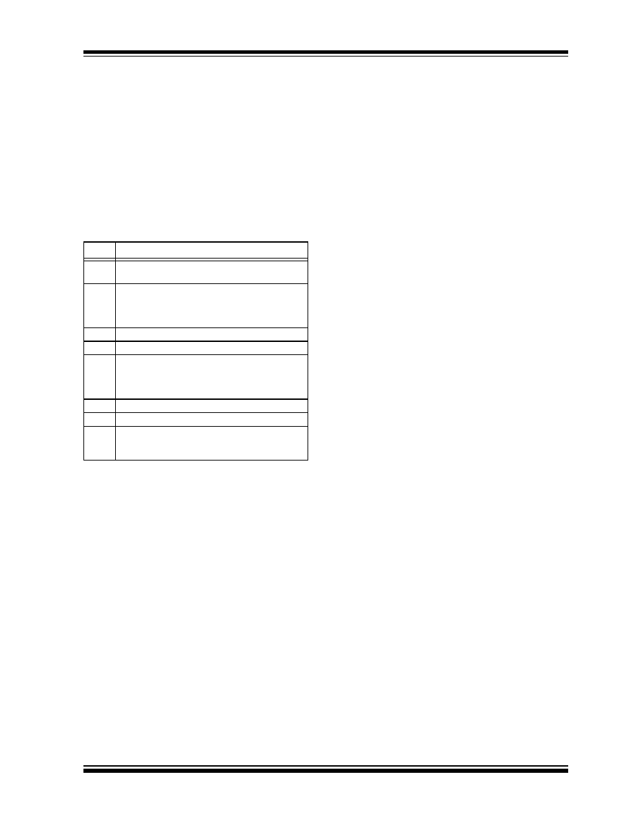
FIGURE 4-11:
TC7129 FUNCTIONAL BLOCK DIAGRAM
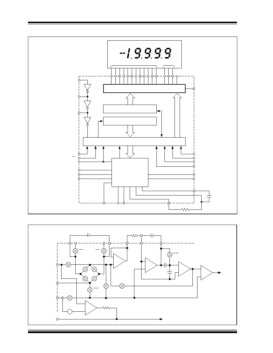
FIGURE 4-12:
INTEGRATOR BLOCK DIAGRAM
Low Battery Continuity
Segment Drives
Backplane
Drives
Latch, Decode Display Multiplexer
Up/Down Results Counter
Sequence Counter/Decoder
Control Logic
Analog Section
OSC1
OSC2
OSC3
RANGE
L/H
CONT
V+
V-
DGND
COMMON
IN
HI
IN
LO
BUFF
DP
1
DP
2
UR/DP
3
OR/DP
4
REF HI
REF LO
INT OUT
INT IN
Annunciator
Drive
V
DISP
TC7129
Common
REF HI
Buffer
Integrator
DE
ZI, X10
Comparator 1
200mV
C
REF
R
INT
C
INT
INT
1
IN HI
+
+
+
REF LO
DE
IN LO
+
DE-
DE+
DE+
DE-
100pF
V
+
Continuity
INT
1
, INT
2
Continuity
Comparator
500k
REST
To Display Driver
10
pF
Comparator 2
To Digital
Section
TC7129
INT
X10
©
2002 Microchip Technology Inc.
DS21459B-page 15
TC7129
4.14
Integrator Section
The integrator section includes the integrator, compar-
ator, input buffer amplifier, and analog switches (see
Table 4-2), used to change the circuit configuration dur-
ing the separate measurement phases described ear-
lier. See Integrator Block Diagram (Figure 4-12).
The buffer amplifier has a Common mode input voltage
range from 1.5V above V- to 1V below V+. The integra-
tor amplifier can swing to within 0.3V of the rails,
although for best linearity, the swing is usually limited to
within 1V. Both amplifiers can supply up to 80
µ
A of out-
put current, but should be limited to 20
µ
A for good
linearity.
4.15
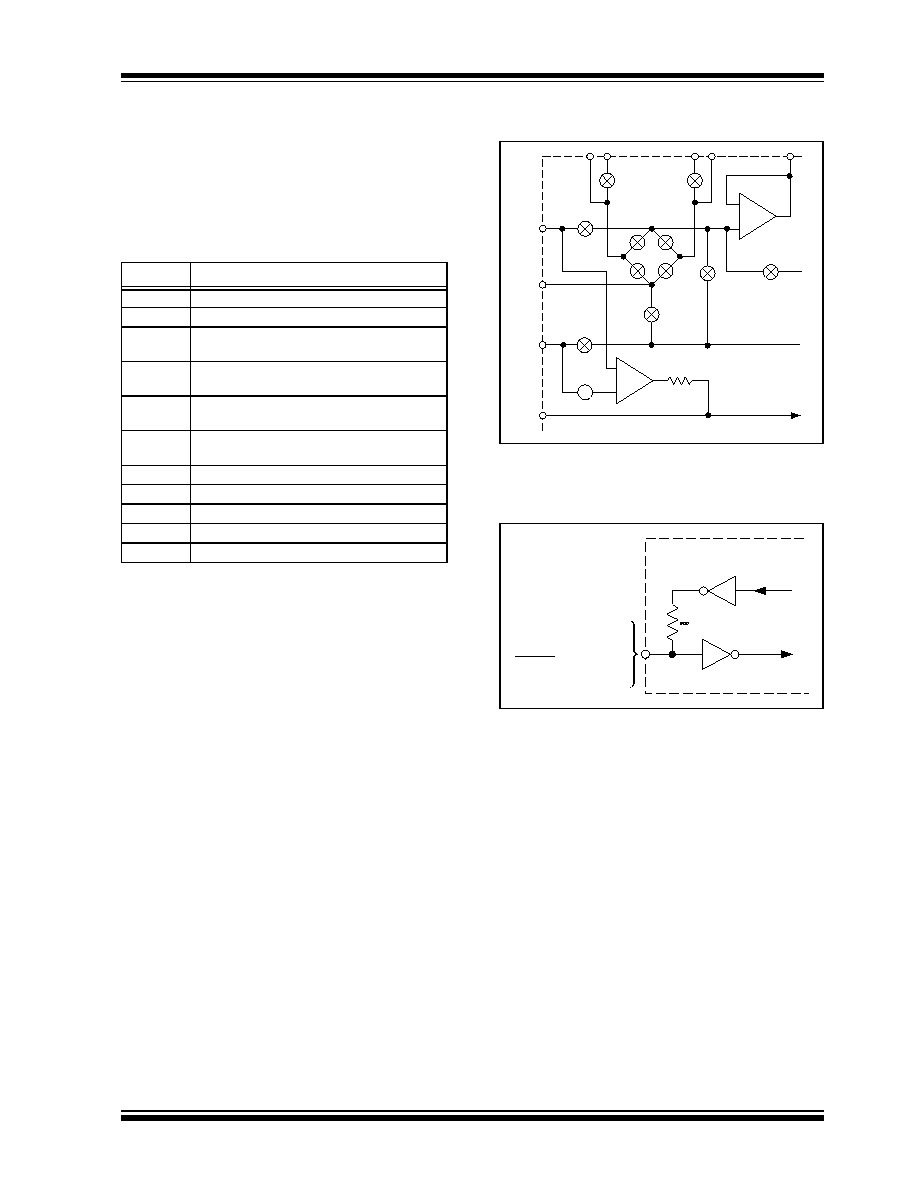
Continuity Indicator
A comparator with a 200mV threshold is connected
between IN HI (Pin 33) and IN LO (Pin 32). Whenever
the voltage between inputs is less than 200mV, the
CONTINUITY output (Pin 27) will be pulled HIGH, acti-
vating the continuity annunciator on the display. The
continuity pin can also be used as an input to drive the
continuity annunciator directly from an external source
(see Figure 4-13).
A schematic of the input/output nature of this pin is also
shown in Figure 4-14.
FIGURE 4-13:
CONTINUITY INDICATOR
CIRCUIT
FIGURE 4-14:
INPUT/OUTPUT PIN
SCHEMATIC
4.16
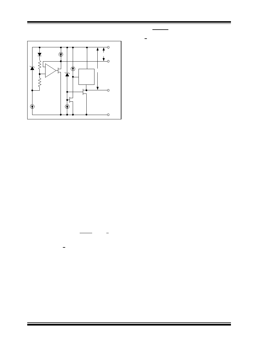
Common and Digital Ground
The common and digital ground (DGND) outputs are
generated from internal zener diodes. The voltage
between V+ and DGND is the internal supply voltage
for the digital section of the TC7129. Common can
source approximately 12
µ
A; DGND has essentially no
source capability (see Figure 4-15).
TABLE 4-2:
SWITCH LEGENDS
Label
Description
Label
Meaning.
DE
Open during all de-integrate phases.
DE
Closed during all de-integrate phases when
input voltage is negative.
DE+
Closed during all de-integrate phases when
input voltage is positive.
INT
1
Closed during the first integrate phase (mea-
surement of the input voltage).
INT
2
Closed during the second integrate phase
(measurement of the amplifier offset).
INT
Open during both integrate phases.
REST
Closed during the rest phase.
ZI
Closed during the zero integrate phase.
X10
Closed during the X10 phase.
X10
Open during the X10 phase.
COM
Buffer
200mV
IN HI
+
IN LO
+
V
CONT
500k
To Display Driver
(Not Latched)
TC7129
TC7129
500k
DP
4
/OR, Pin 20
DP
3
/UR, Pin 21
LATCH/HOLD Pin 22
CONTINUITY, Pin 27
TC7129
DS21459B-page 16
©
2002 Microchip Technology Inc.
FIGURE 4-15:
DIGITAL GROUND (DGND)
AND COMMON OUTPUTS
4.17
Low Battery
The low battery annunciator turns on when supply volt-
age between V- and V+ drops below 6.8V. The internal
zener has a threshold of 6.3V. When the supply voltage
drops below 6.8V, the transistor tied to V- turns OFF,
pulling the "Low Battery" point HIGH.
4.18
Sequence and Results Counter
A sequence counter and associated control logic pro-
vide signals that operate the analog switches in the
integrator section. The comparator output from the inte-
grator gates the results counter. The results counter is
a six-section up/down decade counter, which holds the
intermediate results from each successive integration.
4.19
Over Range and Under Range
Outputs
When the results counter holds a value greater than
±19,999, the DP
4
/OR output (Pin 20) is driven HIGH.
When the results counter value is less than ±1000, the
DP
3
/UR output (Pin 21) is driven HIGH. Both signals
are valid on the falling edge of LATCH/HOLD (L/H) and
do not change until the end of the next conversion
cycle. The signals are updated at the end of each con-
version, unless the L/H input (Pin 22) is held HIGH.
Pins 20 and 21 can also be used as inputs for external
control of decimal points 3 and 4. Figure 4-14 shows a
schematic of the input/output nature of these pins.
4.20
LATCH/Hold
The L/H output goes LOW during the last 100 cycles of
each conversion. This pulse latches the conversion
data into the display driver section of the TC7129. This
pin can also be used as an input. When driven HIGH,
the display will not be updated; the previous reading is
displayed. When driven LOW, the display reading is not
latched; the sequence counter reading will be dis-
played. Since the counter is counting much faster than
the backplanes are being updated, the reading shown
in this mode is somewhat erratic.
4.21
Display Driver
The TC7129 drives a triplexed LCD with three back-
planes. The LCD can include decimal points, polarity
sign, and annunciators for continuity and low battery.
Figure 4-16 shows the assignment of the display seg-
ments to the backplanes and segment drive lines. The
backplane drive frequency is obtained by dividing the
oscillator frequency by 1200. This results in a back-
plane drive frequency of 100Hz for 60Hz operation
(120kHz crystal) and 83.3Hz for 50Hz operation
(100kHz crystal).
Backplane waveforms are shown in Figure 4-17.
These appear on outputs BP
1
, BP
2
, BP
3
(Pins 16, 17,
and 18). They remain the same, regardless of the seg-
ments being driven.
Other display output lines (Pins 4 through 15) have
waveforms that vary depending on the displayed val-
ues. Figure 4-18 shows a set of waveforms for the A, G,
D outputs (Pins 5, 8, 11, and 14) for several combina-
tions of "ON" segments.
The ANNUNCIATOR DRIVE output (Pin 3) is a square
wave, running at the backplane frequency (100Hz or
83.3Hz) with a peak-to-peak voltage equal to DGND
voltage. Connecting an annunciator to Pin 3 turns it
ON; connecting it to its backplane turns it OFF.
+
12
µA
P
TC7129
Logic
Section
5V
3.2V
N
N
V+
V-
COM
DGND
24
28
36
23
©
2002 Microchip Technology Inc.
DS21459B-page 17
TC7129
FIGURE 4-16:
DISPLAY SEGMENT ASSIGNMENTS
FIGURE 4-17:
BACKPLANE
WAVEFORMS
FIGURE 4-18:
TYPICAL DISPLAY
OUTPUT WAVEFORMS
BP
1
BP
2
BP
3
Low Battery
Low Battery
Continuity
F
4
, E
4
, DP
4
A
4
, G
4
, D
4
B
4
, C
4
, BC
4
F
3
, E
3
, DP
3
A
3
, G
3
, D
3
B
3
, C
3
, MINUS
B
1
, C
1
, Continuity
A
1
, G
1
, D
1
F
1
, E
1
, DP
1
B
2
, C
2
, Low Battery
A
2
, G
2
, D
2
Backplane
Connections
F
2
, E
2
, DP
2
Continuity
BP
1
BP2
BP
3
V
DD
V
H
V
L
V
DISP
V
DD
V
H
V
L
V
DISP
V
DD
V
H
V
L
V
DISP
V
DD
V
H
V
L
V
DISP
b Segment
Line
All Off
a Segment
On
d, g Off
a, g On
d Off
All On
TC7129
DS21459B-page 18
©
2002 Microchip Technology Inc.
5.0
PACKAGING INFORMATION
5.1
Package Marking Information
Package marking data not available a this time.
5.2
Taping Forms
PIN 1
Component Taping Orientation for 44-Pin PLCC Devices
User Direction of Feed
Standard Reel Component Orientation
for TR Suffix Device
Note: Drawing does not represent total number of pins.
W
P
Package
Carrier Width (W)
Pitch (P)
Part Per Full Reel
Reel Size
44-Pin PLCC
32 mm
24 mm
500
13 in
Carrier Tape, Number of Components Per Reel and Reel Size
Component Taping Orientation for 44-Pin PQFP Devices
User Direction of Feed
PIN 1
Standard Reel Component Orientation
for TR Suffix Device
W
P
Package
Carrier Width (W)
Pitch (P)
Part Per Full Reel
Reel Size
44-Pin PQFP
24 mm
16 mm
500
13 in
Carrier Tape, Number of Components Per Reel and Reel Size
Note: Drawing does not represent total number of pins.
©
2002 Microchip Technology Inc.
DS21459B-page 19
TC7129
5.3
Package Dimensions
Dimensions: inches (mm)
2.065 (52.45)
2.027 (51.49)
.200 (5.08)
.140 (3.56)
.150 (3.81)
.115 (2.92)
.070 (1.78)
.045 (1.14)
.022 (0.56)
.015 (0.38)
.110 (2.79)
.090 (2.29)
.555 (14.10)
.530 (13.46)
.610 (15.49)
.590 (14.99)
.015 (0.38)
.008 (0.20)
.700 (17.78)
.610 (15.50)
.040 (1.02)
.020 (0.51)
40-Pin PDIP (Wide)
PIN 1
3
° MIN.
Dimensions: inches (mm)
.695 (17.65)
.685 (17.40)
.656 (16.66)
.650 (16.51)
.656 (16.66)
.650 (16.51)
.021 (0.53)
.013 (0.33)
.032 (0.81)
.026 (0.66)
.630 (16.00)
.591 (15.00)
.120 (3.05)
.090 (2.29)
.180 (4.57)
.165 (4.19)
.695 (17.65)
.685 (17.40)
.050 (1.27) TYP.
.020 (0.51) MIN.
PIN 1
44-Pin PLCC
TC7129
DS21459B-page 20
©
2002 Microchip Technology Inc.
5.3
Package Dimensions (Continued)
Dimensions: inches (mm)
.557 (14.15)
.537 (13.65)
.398 (10.10)
.390 (9.90)
.031 (0.80) TYP.
.018 (0.45)
.012 (0.30)
.398 (10.10)
.390 (9.90)
.010 (0.25) TYP.
.096 (2.45) MAX.
.557 (14.15)
.537 (13.65)
.083 (2.10)
.075 (1.90)
.041 (1.03)
.026 (0.65)
7
° MAX.
.009 (0.23)
.005 (0.13)
44-Pin PQFP
PIN 1

©
2002 Microchip Technology Inc.
DS21459B-page 21
TC7129
NOTES:

TC7129
DS21459B-page 22
©
2002 Microchip Technology Inc.
SALES AND SUPPORT
Data Sheets
Products supported by a preliminary Data Sheet may have an errata sheet describing minor operational differences and recom-
mended workarounds. To determine if an errata sheet exists for a particular device, please contact one of the following:
1.
Your local Microchip sales office
2.
The Microchip Corporate Literature Center U.S. FAX: (480) 792-7277
3.
The Microchip Worldwide Site (www.microchip.com)
Please specify which device, revision of silicon and Data Sheet (include Literature #) you are using.
New Customer Notification System
Register on our web site (www.microchip.com/cn) to receive the most current information on our products.

©
2002 Microchip Technology Inc.
DS21459B-page 23
TC7129
Information contained in this publication regarding device
applications and the like is intended through suggestion only
and may be superseded by updates. It is your responsibility to
ensure that your application meets with your specifications.
No representation or warranty is given and no liability is
assumed by Microchip Technology Incorporated with respect
to the accuracy or use of such information, or infringement of
patents or other intellectual property rights arising from such
use or otherwise. Use of Microchip's products as critical com-
ponents in life support systems is not authorized except with
express written approval by Microchip. No licenses are con-
veyed, implicitly or otherwise, under any intellectual property
rights.
Trademarks
The Microchip name and logo, the Microchip logo, FilterLab,
K
EE
L
OQ
, microID,
MPLAB, PIC, PICmicro, PICMASTER,
PICSTART, PRO MATE, SEEVAL and The Embedded Control
Solutions Company are registered trademarks of Microchip Tech-
nology Incorporated in the U.S.A. and other countries.
dsPIC, ECONOMONITOR, FanSense, FlexROM, fuzzyLAB,
In-Circuit Serial Programming, ICSP, ICEPIC, microPort,
Migratable Memory, MPASM, MPLIB, MPLINK, MPSIM,
MXDEV, PICC, PICDEM, PICDEM.net, rfPIC, Select Mode
and Total Endurance are trademarks of Microchip Technology
Incorporated in the U.S.A.
Serialized Quick Turn Programming (SQTP) is a service mark
of Microchip Technology Incorporated in the U.S.A.
All other trademarks mentioned herein are property of their
respective companies.
© 2002, Microchip Technology Incorporated, Printed in the
U.S.A., All Rights Reserved.
Printed on recycled paper.
Microchip received QS-9000 quality system
certification for its worldwide headquarters,
design and wafer fabrication facilities in
Chandler and Tempe, Arizona in July 1999
and Mountain View, California in March 2002.
The Company's quality system processes and
procedures are QS-9000 compliant for its
PICmicro
®
8-bit MCUs, K
EE
L
OQ
®
code hopping
devices, Serial EEPROMs, microperipherals,
non-volatile memory and analog products. In
addition, Microchip's quality system for the
design and manufacture of development
systems is ISO 9001 certified.

DS21459B-page 24
©
2002 Microchip Technology Inc.
AMERICAS
Corporate Office
2355 West Chandler Blvd.
Chandler, AZ 85224-6199
Tel: 480-792-7200 Fax: 480-792-7277
Technical Support: 480-792-7627
Web Address: http://www.microchip.com
Rocky Mountain
2355 West Chandler Blvd.
Chandler, AZ 85224-6199
Tel: 480-792-7966 Fax: 480-792-7456
Atlanta
500 Sugar Mill Road, Suite 200B
Atlanta, GA 30350
Tel: 770-640-0034 Fax: 770-640-0307
Boston
2 Lan Drive, Suite 120
Westford, MA 01886
Tel: 978-692-3848 Fax: 978-692-3821
Chicago
333 Pierce Road, Suite 180
Itasca, IL 60143
Tel: 630-285-0071 Fax: 630-285-0075
Dallas
4570 Westgrove Drive, Suite 160
Addison, TX 75001
Tel: 972-818-7423 Fax: 972-818-2924
Detroit
Tri-Atria Office Building
32255 Northwestern Highway, Suite 190
Farmington Hills, MI 48334
Tel: 248-538-2250 Fax: 248-538-2260
Kokomo
2767 S. Albright Road
Kokomo, Indiana 46902
Tel: 765-864-8360 Fax: 765-864-8387
Los Angeles
18201 Von Karman, Suite 1090
Irvine, CA 92612
Tel: 949-263-1888 Fax: 949-263-1338
New York
150 Motor Parkway, Suite 202
Hauppauge, NY 11788
Tel: 631-273-5305 Fax: 631-273-5335
San Jose
Microchip Technology Inc.
2107 North First Street, Suite 590
San Jose, CA 95131
Tel: 408-436-7950 Fax: 408-436-7955
Toronto
6285 Northam Drive, Suite 108
Mississauga, Ontario L4V 1X5, Canada
Tel: 905-673-0699 Fax: 905-673-6509
ASIA/PACIFIC
Australia
Microchip Technology Australia Pty Ltd
Suite 22, 41 Rawson Street
Epping 2121, NSW
Australia
Tel: 61-2-9868-6733 Fax: 61-2-9868-6755
China - Beijing
Microchip Technology Consulting (Shanghai)
Co., Ltd., Beijing Liaison Office
Unit 915
Bei Hai Wan Tai Bldg.
No. 6 Chaoyangmen Beidajie
Beijing, 100027, No. China
Tel: 86-10-85282100 Fax: 86-10-85282104
China - Chengdu
Microchip Technology Consulting (Shanghai)
Co., Ltd., Chengdu Liaison Office
Rm. 2401, 24th Floor,
Ming Xing Financial Tower
No. 88 TIDU Street
Chengdu 610016, China
Tel: 86-28-6766200 Fax: 86-28-6766599
China - Fuzhou
Microchip Technology Consulting (Shanghai)
Co., Ltd., Fuzhou Liaison Office
Unit 28F, World Trade Plaza
No. 71 Wusi Road
Fuzhou 350001, China
Tel: 86-591-7503506 Fax: 86-591-7503521
China - Shanghai
Microchip Technology Consulting (Shanghai)
Co., Ltd.
Room 701, Bldg. B
Far East International Plaza
No. 317 Xian Xia Road
Shanghai, 200051
Tel: 86-21-6275-5700 Fax: 86-21-6275-5060
China - Shenzhen
Microchip Technology Consulting (Shanghai)
Co., Ltd., Shenzhen Liaison Office
Rm. 1315, 13/F, Shenzhen Kerry Centre,
Renminnan Lu
Shenzhen 518001, China
Tel: 86-755-2350361 Fax: 86-755-2366086
Hong Kong
Microchip Technology Hongkong Ltd.
Unit 901-6, Tower 2, Metroplaza
223 Hing Fong Road
Kwai Fong, N.T., Hong Kong
Tel: 852-2401-1200 Fax: 852-2401-3431
India
Microchip Technology Inc.
India Liaison Office
Divyasree Chambers
1 Floor, Wing A (A3/A4)
No. 11, O'Shaugnessey Road
Bangalore, 560 025, India
Tel: 91-80-2290061 Fax: 91-80-2290062
Japan
Microchip Technology Japan K.K.
Benex S-1 6F
3-18-20, Shinyokohama
Kohoku-Ku, Yokohama-shi
Kanagawa, 222-0033, Japan
Tel: 81-45-471- 6166 Fax: 81-45-471-6122
Korea
Microchip Technology Korea
168-1, Youngbo Bldg. 3 Floor
Samsung-Dong, Kangnam-Ku
Seoul, Korea 135-882
Tel: 82-2-554-7200 Fax: 82-2-558-5934
Singapore
Microchip Technology Singapore Pte Ltd.
200 Middle Road
#07-02 Prime Centre
Singapore, 188980
Tel: 65-6334-8870 Fax: 65-6334-8850
Taiwan
Microchip Technology Taiwan
11F-3, No. 207
Tung Hua North Road
Taipei, 105, Taiwan
Tel: 886-2-2717-7175 Fax: 886-2-2545-0139
EUROPE
Denmark
Microchip Technology Nordic ApS
Regus Business Centre
Lautrup hoj 1-3
Ballerup DK-2750 Denmark
Tel: 45 4420 9895 Fax: 45 4420 9910
France
Microchip Technology SARL
Parc d'Activite du Moulin de Massy
43 Rue du Saule Trapu
Batiment A - ler Etage
91300 Massy, France
Tel: 33-1-69-53-63-20 Fax: 33-1-69-30-90-79
Germany
Microchip Technology GmbH
Gustav-Heinemann Ring 125
D-81739 Munich, Germany
Tel: 49-89-627-144 0 Fax: 49-89-627-144-44
Italy
Microchip Technology SRL
Centro Direzionale Colleoni
Palazzo Taurus 1 V. Le Colleoni 1
20041 Agrate Brianza
Milan, Italy
Tel: 39-039-65791-1 Fax: 39-039-6899883
United Kingdom
Arizona Microchip Technology Ltd.
505 Eskdale Road
Winnersh Triangle
Wokingham
Berkshire, England RG41 5TU
Tel: 44 118 921 5869 Fax: 44-118 921-5820
03/01/02
*DS21459B*
W
ORLDWIDE
S
ALES
AND
S
ERVICE