 | –≠–ª–µ–∫—Ç—Ä–æ–Ω–Ω—ã–π –∫–æ–º–ø–æ–Ω–µ–Ω—Ç: TC7135CLI | –°–∫–∞—á–∞—Ç—å:  PDF PDF  ZIP ZIP |
©
2002 Microchip Technology Inc.
DS21460B-page 1
TC7135
Features
∑ Low Rollover Error: ±1 Count Max
∑ Nonlinearity Error: ±1 Count Max
∑ Reading for 0V Input
∑ True Polarity Indication at Zero for Null Detection
∑ Multiplexed BCD Data Output
∑ TTL-Compatible Outputs
∑ Differential Input
∑ Control Signals Permit Interface to UARTs and
Microprocessors
∑ Blinking Display Visually Indicates Overrange
Condition
∑ Low Input Current: 1pA
∑ Low Zero Reading Drift: 2
µ
V/∞C
∑ Auto-Ranging Supported with Overrange and
Underrange Signals
∑ Available in PDIP and Surface-Mount Packages
Applications
∑ Precision Analog Signal Processor
∑ Precision Sensor Interface
∑ High Accuracy DC Measurements
Device Selection Table
General Description
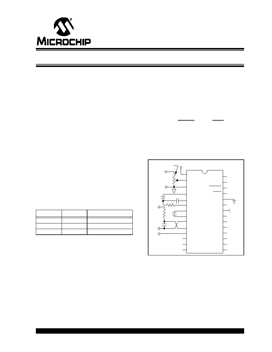
The TC7135 4-1/2 digit A/D converter (ADC) offers
50ppm (1 part in 20,000) resolution with a maximum
nonlinearity error of 1 count. An auto zero cycle
reduces zero error to below 10
µ
V and zero drift to
0.5
µ
V/∞C. Source impedance errors are minimized by
a 10pA maximum input current. Rollover error is limited
to ±1 count.
Microprocessor based measurement systems are sup-
ported by BUSY, STROBE and RUN/HOLD control sig-
nals. Remote data acquisition systems with data
transfer via UARTs are also possible. The additional
control pins and multiplexed BCD outputs make the
TC7135
the
ideal
converter
for
display
or
microprocessor based measurement systems.
Functional Block Diagram
Part Number
Package
Temperature Range
TC7135CLI
28-Pin PLCC
0
∞
C to +70
∞
C
TC7135CPI
28-Pin PDIP
0
∞
C to +70
∞
C
TC7135CBU
64-Pin PQFP
0
∞
C to +70
∞
C
TC7135
1
2
3
4
5
6
7
8
9
10
11
12
13
14
28
27
26
25
24
23
22
21
20
19
18
17
16
15
100k
Analog GND
100
k
Signal
Input
0.1
µF
SET V
REF
= 1V
V-
REF IN
ANALOG
COMMON
INT OUT
AZ IN
BUFF OUT
C
REF
-
C
REF
+
-INPUT
+INPUT
D5 (MSD)
B1 (LSB)
B2
V+
UNDERRANGE
OVERRANGE
STROBE
RUN/HOLD
DIGTAL GND
POLARITY
CLOCK IN
BUSY
(LSD) D1
D2
D4
(MSB) B8
B4
D3
+5V
1
µF
100k
1
µF
0.47
µF
V
REF
IN
Clock
Input
120kHz
≠5V
4-1/2 Digit A/D Converter
TC7135
DS21460B-page 2
©
2002 Microchip Technology Inc.
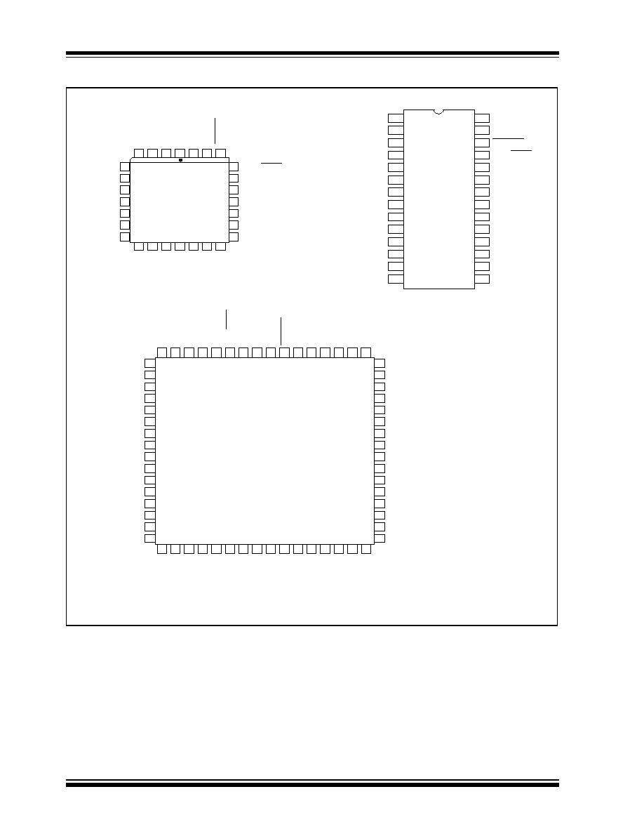
Package Types
NOTE: NC = No internal connection.
TC7135
1
2
3
4
5
6
7
8
9
10
11
12
13
14
28
27
26
25
24
23
22
21
20
19
18
17
16
15
OVERRANGE
B4
D3
D2
D1 (LSD)
BUSY
CLOCK IN
POLARITY
DIGTAL GND
UNDERRANGE
B2
(LSB) B1
(MSD) D5
V+
+INPUT
≠ INPUT
C
REF
+
C
REF
-
BUFF OUT
AZ IN
INT OUT
ANALOG
COM
REF IN
V-
STROBE
RUN/HOLD
D4
B8 (MSB)
28-Pin PDIP
28-Pin PDIP
19
20
21
22
23
24
25
11
10
9
8
7
6
5
CLOCK IN
RUN/HOLD
TC7135
AZ IN
POLARITY
12 13 14 15
17 18
(MSD) D5
(LSB) B1
B2
B4
(MSB) B8
D4
D3
DIGTAL GND
BUSY
D1 (LSD)
D2
BUFF OUT
REF CAP≠
REF CAP+
≠INPUT
V +
4
3
2
1
27 26
28
INT OUT
ANALOG
COM
REF IN
V
≠
UR
OR
STROBE
16
+INPUT
4
3
2
16
15
14
10
9
8
7
6
5
12
11
17 18 19 20 21 22 23 24 25 26 27 28 29 30 31
TC7135
64-Pin PQFP
NC
INT OUT
NC
AZ IN
NC
NC
NC
C
REF
+
C
REF
-
NC
≠
INPUT
NC
+INPUT
NC
V+
l
32
BUFF OUT
NC
BUSY
D2
D1
63
61 60 59 58 57 56 55 54 53 52 51 50 49
64
NC
NC
NC
NC
NC
DGND
POL
NC
CLOCK IN
62
NC
NC
NC
NC
NC
NC
OVERRANGE
UNDERRANGE
NC
V-
REF IN
ANALOG COM
NC
NC
NC
NC
NC
NC
D5
NC
NC
NC
NC
D3
NC
NC
D4
B8
B4
B2
NC
B1
NC
13
40
41
42
43
44
45
46
34
35
36
37
38
39
33
48
47
1
RUN/HOLD
STROBE

©
2002 Microchip Technology Inc.
DS21460B-page 3
TC7135
1.0
ELECTRICAL SPECIFICATIONS
Absolute Maximum Ratings*
Positive Supply Voltage..........................................+6V
Negative Supply Voltage ....................................... - 9V
Analog Input Voltage (Pin 9 or 10) .... V+ to V- (Note 2)
Reference Input Voltage (Pin 2) ...................... V+ to V-
Clock Input Voltage ........................................ 0V to V+
Operating Temperature Range ............... 0∞C to +70∞C
Storage Temperature Range ............ ≠ 65∞C to +150∞C
Package Power Dissipation; (T
A
70∞C)
28-Pin PDIP ..................................... 1.14
28-Pin PLCC .................................... 1.00
64-Pin PQFP .....................................1.14
*Stresses above those listed under "Absolute Maximum Rat-
ings" may cause permanent damage to the device. These are
stress ratings only and functional operation of the device at
these or any other conditions above those indicated in the
operation sections of the specifications is not implied. Expo-
sure to Absolute Maximum Rating conditions for extended
periods may affect device reliability.
TC7135 ELECTRICAL SPECIFICATIONS
Electrical Characteristics: T
A
= +25∞C, F
CLOCK
= 120kHz, V+ = +5V, V- = -5V, unless otherwise specified
(see Functional Block Diagram).
Symbol
Parameter
Min
Typ
Max
Unit
Test Conditions
Analog
Display Reading with Zero Volt Input
-0.0000
±0.0000
+0.0000
Display Reading
Note 2 and Note 3
TC
Z
Zero Reading Temperature Coefficient
--
0.5
2
µ
V/∞C
V
IN
= 0V, (Note 4)
TC
FS
Full Scale Temperature Coefficient
--
--
5
ppm/∞C
V
IN
= 2V,
(Note 4 and Note 5)
NL
Nonlinearity Error
--
0.5
1
Count
Note 6
DNL
Differential Linearity Error
--
0.01
--
LSB
Note 6
Display Reading in Ratiometric Operation
+0.9996
+0.9999
+1.0000
Display Reading
V
IN
= V
REF,
(Note 2)
±FSE
± Full Scale Symmetry Error
(Rollover Error)
--
0.5
1
Count
-V
IN
= +V
IN,
(Note 7)
I
IN
Input Leakage Current
--
1
10
pA
Note 3
e
N
Noise
--
15
--
µ
V
P-P
Peak-to-Peak Value not
Exceeded 95% of Time
Digital
I
IL
Input Low Current
--
10
100
µ
A
V
IN
= 0V
I
IH
Input High Current
--
0.08
10
µ
A
V
IN
= +5V
V
OL
Output Low Voltage
--
0.2
0.4
V
I
OL
= 1.6mA
V
OH
Output High Voltage;
B
1
, B
2
, B
4
, B
8
, D
1 ≠
D
5
Busy, Polarity, Overrange,
Underrange, Strobe
2.4
4.4
5
V
I
OH
= 1mA
4.9
4.99
5
V
I
OH
= 10
µ
A
F
CLK
Clock Frequency
0
200
1200
kHz
Note 8
Note
1:
Limit input current to under 100
µ
A if input voltages exceed supply voltage.
2:
Full scale voltage = 2V.
3:
V
IN
= 0V.
4:
30∞C
T
A
+70∞C
5:
.External reference temperature coefficient less than 0.01ppm/∞C.
6:
-2V
V
IN
+2V. Error of reading from best fit straight line.
7:
IV
IN
| = 1.9959.
8:
Specification related to clock frequency range over which the TC7135 correctly performs its various functions. Increased
errors result at higher operating frequencies.
TC7135
DS21460B-page 4
©
2002 Microchip Technology Inc.
Power Supply
V+
Positive Supply Voltage
4
5
6
V
V-
Negative Supply Voltage
-3
-5
-8
V
I+
Positive Supply Current
--
1
3
mA
F
CLK
= 0Hz
I-
Negative Supply Current
--
0.7
3
mA
F
CLK
= 0Hz
PD
Power Dissipation
--
8.5
30
mW
F
CLK
= 0Hz
TC7135 ELECTRICAL SPECIFICATIONS (CONTINUED)
Electrical Characteristics: T
A
= +25∞C, F
CLOCK
= 120kHz, V+ = +5V, V- = -5V, unless otherwise specified
(see Functional Block Diagram).
Symbol
Parameter
Min
Typ
Max
Unit
Test Conditions
Note
1:
Limit input current to under 100
µ
A if input voltages exceed supply voltage.
2:
Full scale voltage = 2V.
3:
V
IN
= 0V.
4:
30∞C
T
A
+70∞C
5:
.External reference temperature coefficient less than 0.01ppm/∞C.
6:
-2V
V
IN
+2V. Error of reading from best fit straight line.
7:
IV
IN
| = 1.9959.
8:
Specification related to clock frequency range over which the TC7135 correctly performs its various functions. Increased
errors result at higher operating frequencies.

©
2002 Microchip Technology Inc.
DS21460B-page 5
TC7135
2.0
PIN DESCRIPTIONS
The description of the pins are listed in Table 2-1.
TABLE 2-1:
PIN FUNCTION TABLE
Pin Number
28-Pin PDIP
Symbol
Description
1
V-
Negative power supply input.
2
REF IN
External reference input.
3
ANALOG COMMON
Reference point for REF IN.
4
INT OUT
Integrator output. Integrator capacitor connection.
5
AZ IN
Auto zero inpt. Auto-zero capacitor connection.
6
BUFF OUT
Analog input buffer output. Integrator resistor connection.
7
C
REF
-
Reference capacitor input. Reference capacitor negative connection.
8
C
REF
+
Reference capacitor input. Reference capacitor positive connection.
9
-INPUT
Analog input. Analog input negative connection.
10
+INPUT
Analog input. Analog input positive connection.
11
V+
Positive power supply input.
12
D5
Digit drive output. Most Significant Digit (MSD)
13
B1
Binary Coded Decimal (BCD) output. Least Significant Bit (LSB)
14
B2
BCD output.
15
B4
BCD output.
16
B8
BCD output. Most Significant Bit (MSB)
17
D4
Digit drive output.
18
D3
Digit drive output.
19
D2
Digit drive output.
20
D1
Digit drive output. Least Significant Digit (LSD)
21
BUSY
Busy output. At the beginning of the signal-integration phase, BUSY goes High and
remains High until the first clock pulse after the integrator zero crossing.
22
CLOCK IN
Clock input. Conversion clock connection.
23
POLARITY
Polarity output. A positive input is indicated by a logic High output. The polarity output is
valid at the beginning of the reference integrate phase and remains valid until determined
during the next conversion.
24
DGND
Digital logic reference input.
25
RUN/HOLD
Run / Hold input. When at a logic High, conversions are performed continuously. A logic
Low holds the current data as long as the Low condition exists.
26
STROBE
Strobe output. The STROBE output pulses low in the center of the digit drive outputs.
27
OVERRANGE
Over range output. A logic High indicates that the analog input exceeds the full scale input
range.
28
UNDERRANGE
Under range output. A logic High indicates that the analog input is less than 9% of the full
scale input range.