 | ÐлекÑÑоннÑй компоненÑ: TC7650CPD | СкаÑаÑÑ:  PDF PDF  ZIP ZIP |
Äîêóìåíòàöèÿ è îïèñàíèÿ www.docs.chipfind.ru
©
2002 Microchip Technology Inc.
DS21463B-page 1
Features
· Low Input Offset Voltage: 0.7µV Typ
· Low Input Offset Voltage Drift: 0.05
µ
V/°C Max
· Low Input Bias Current: 10pA Max
· High Impedance Differential CMOS Inputs: 10
12
· High Open Loop Voltage Gain: 120dB Min.
· Low Input Noise Voltage: 2.0
µ
Vp-p
· High Slew Rate: 2.5V/
µ
sec.
· Low Power Operation: 20mW
· Output Clamp Speeds Recovery Time
· Compensated Internally for Stable Unity Gain
Operation
· Direct Replacement for ICL7650
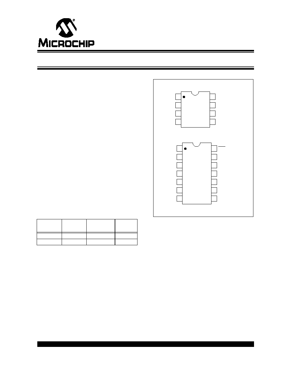
· Available in 8-Pin Plastic DIP and 14-Pin Plastic
DIP Packages
Applications
· Instrumentation
· Medical Instrumentation
· Embedded Control
· Temperature Sensor Amplifier
· Strain Gage Amplifier
Device Selection Table
Package Type
Part
Number
Package
Temperature
Range
Max V
OS
TC7650CPA
8-Pin PDIP
0°C to +70°C
5
µ
V
TC7650CPD 14-Pin PDIP
0°C to +70°C
5
µ
V
1
2
3
4
5
6
7
14
13
12
11
10
9
8
C
B
NC
8-Pin DIP
V
SS
V
SS
INT/EXT
EXT CLK IN
INT CLK OUT
OUTPUT
OUTPUT CLAMP
C
A
C
RETN
V
DD
TC7650CPD
1
2
3
4
8
7
6
5
C
A
OUTPUT
V
DD
TC7650CPA
INPUT
INPUT
C
B
+
OUTPUT CLAMP
INPUT
INPUT
+
NC
14-Pin DIP
NC = NO INTERNAL CONNECTION
TC7650
Chopper Stabilized Operational Amplifier
TC7650
DS21463B-page 2
©
2002 Microchip Technology Inc.
General Description
The TC7650 CMOS chopper stabilized operational
amplifier practically removes offset voltage error terms
from system error calculations. The 5
µ
V maximum V
OS
specification, for example, represents a 15 times
improvement over the industry standard OP07E. The
50nV/°C offset drift specification is over 25 times lower
than the OP07E. The increased performance elimi-
nates V
OS
trim procedures, periodic potentiometer
adjustment and the reliability problems caused by dam-
aged trimmers.
The TC7650 performance advantages are achieved
without the additional manufacturing complexity and
cost incurred with laser or "zener zap" V
OS
trim tech-
niques.
The TC7650 nulling scheme corrects both DC V
OS
errors and V
OS
drift errors with temperature. A nulling
amplifier alternately corrects its own V
OS
errors and the
main amplifier V
OS
error. Offset nulling voltages are
stored on two user supplied external capacitors. The
capacitors connect to the internal amplifier V
OS
null
points. The main amplifier input signal is never
switched. Switching spikes are not present at the
TC7650 output.
The 14-pin dual-in-line package (DIP) has an external
oscillator input to drive the nulling circuitry for optimum
noise performance. Both the 8 and 14-pin DIPs have
an output voltage clamp circuit to minimize overload
recovery time.
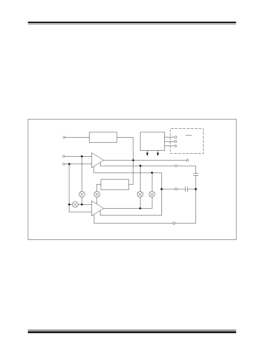
Functional Block Diagram
TC7650
Null
NULL
Inputs
Output
Clamp
Output
B
B
A
C
A
C
B
For 8-Pin DIP, connect to Vss
Null
Amplifier
Main
Amplifier
Output Clamp
Circuit
Intermod
Compensation
Oscillator
A
B
INT/EXT
EXT CLK IN
CLK OUT
14-Pin DIP Only
B
A
*C
RETN
*
©
2002 Microchip Technology Inc.
DS21463B-page 3
TC7650
1.0
ELECTRICAL
CHARACTERISTICS
ABSOLUTE MAXIMUM RATINGS*
Total Supply Voltage (V
DD
to V
SS
) .......................+18V
Input Voltage .................... (V
DD
+0.3V) to (V
SS
0.3V)
Storage Temperature Range .............. -65°C to +150°C
Voltage on Oscillator Control Pins...............V
DD
to V
SS
Duration of Output Short Circuit ..................... Indefinite
Current Into Any Pin............................................ 10mA
While Operating (Note 3)............................ 100µA
Package Power Dissipation (T
A
70°C)
8-Pin Plastic DIP ....................................... 730mW
14-Pin Plastic DIP ..................................... 800mW
Operating Temperature Range
C Device .......................................... 0°C to +70°C
*Stresses above those listed under "Absolute Maximum
Ratings" may cause permanent damage to the device.
These are stress ratings only and functional operation of the
device at these or any other conditions above those indi-
cated in the operation sections of the specifications is not
implied. Exposure to Absolute Maximum Rating conditions
for extended periods my affect device reliability.
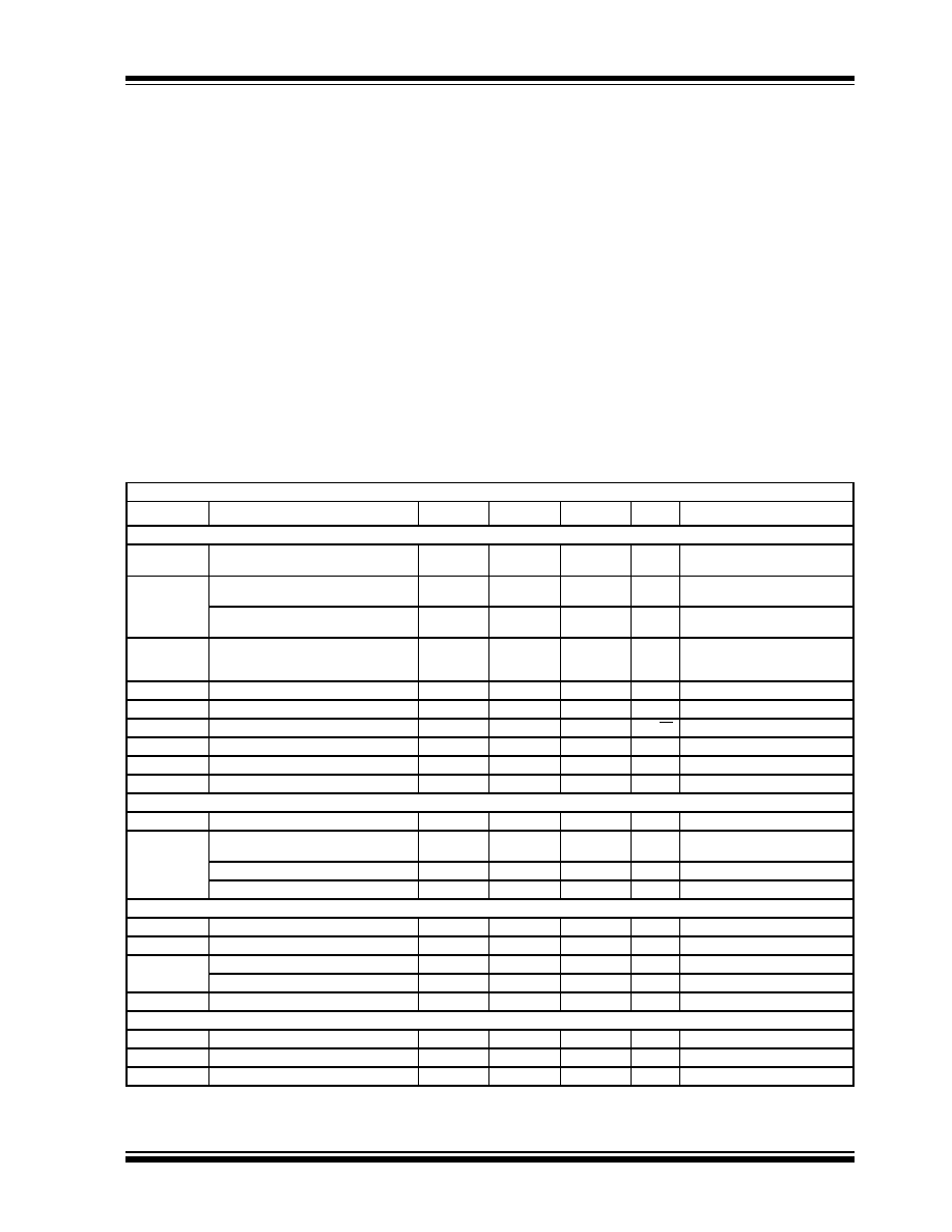
TC7652 ELECTRICAL SPECIFICATIONS
Electrical Characteristics: V
DD
= +5V, V
SS
= -5V, C
A
= C
B
= 0.1
µ
F, T
A
= +25°C, unless otherwise indicated.
Symbol
Parameter
Min.
Typ
Max
Units
Test Conditions
Input
V
OS
Input Offset Voltage
--
--
±0.7
±1.0
±5
--
--
µ
V
T
A
= +25°C
Over Operating Temp Range
V
OS
/
T
Input Offset Voltage Average
Temperature Coefficient
--
0.01
0.05
µ
V/°C
Operating Temperature Range
Offset Voltage vs. Time
--
100
--
nV/
month
I
BIAS
Input Bias Current
--
--
--
1.5
35
100
10
150
400
pA
pA
pA
T
A
= +25°C
0°C
T
A
+70°C
-25°C
T
A
+85°C
I
OS
Input Offset Current
--
0.5
--
pA
e
NP-P
Input Noise Voltage
--
2
--
µ
V
P-P
R
S
= 100
, 0 to 10Hz
I
N
Input Noise Current
--
0.01
--
pA/
Hz
f = 10Hz
R
IN
Input Resistance
--
10
12
CMVR
Common Mode Voltage Range
-5
-5.2 to +2
+1.6
V
CMRR
Common Mode Rejection Ratio
120
130
--
dB
CMVR = -5V to +1.5V
Output
A
Large Signal Voltage Gain
120
130
--
dB
R
L
= 10k
V
OUT
Output Voltage Swing (Note 2)
±4.7
--
±4.85
±4.95
--
--
V
V
R
L
= 10k
R
L
= 100k
Clamp ON Current
25
70
200
µ
A
R
L
= 100k
(Note 1)
Clamp OFF Current
--
1
--
pA
-4V < V
OUT
< +4V (Note 1)
Dynamic
B
W
Unity Gain Bandwidth
--
2.0
--
MHz
Unity Gain (+1)
S
R
Slew Rate
--
2.5
--
V/
µ
sec
C
L
= 50pF, R
L
= 10k
t
R
Rise Time
--
0.2
--
µ
sec
Overshoot
--
20
--
%
f
CH
Internal Chopping Frequency
120
200
375
Hz
Pins 1214 Open (DIP)
Supply
V
DD
, V
SS
Operating Supply Range
4.5
--
16
V
I
S
Supply Current
--
2
3.5
mA
No Load
PSRR
Power Supply Rejection Ratio
120
130
dB
V
S
= ±3V to ±8V
Note
1:
See "Output Clamp" discussion.
2:
Output clamp not connected. See typical characteristics curves for output swing versus clamp current characteristics.
3:
Limiting input current to 100
µ
A is recommended to avoid latch-up problems.
TC7650
DS21463B-page 4
©
2002 Microchip Technology Inc.
2.0
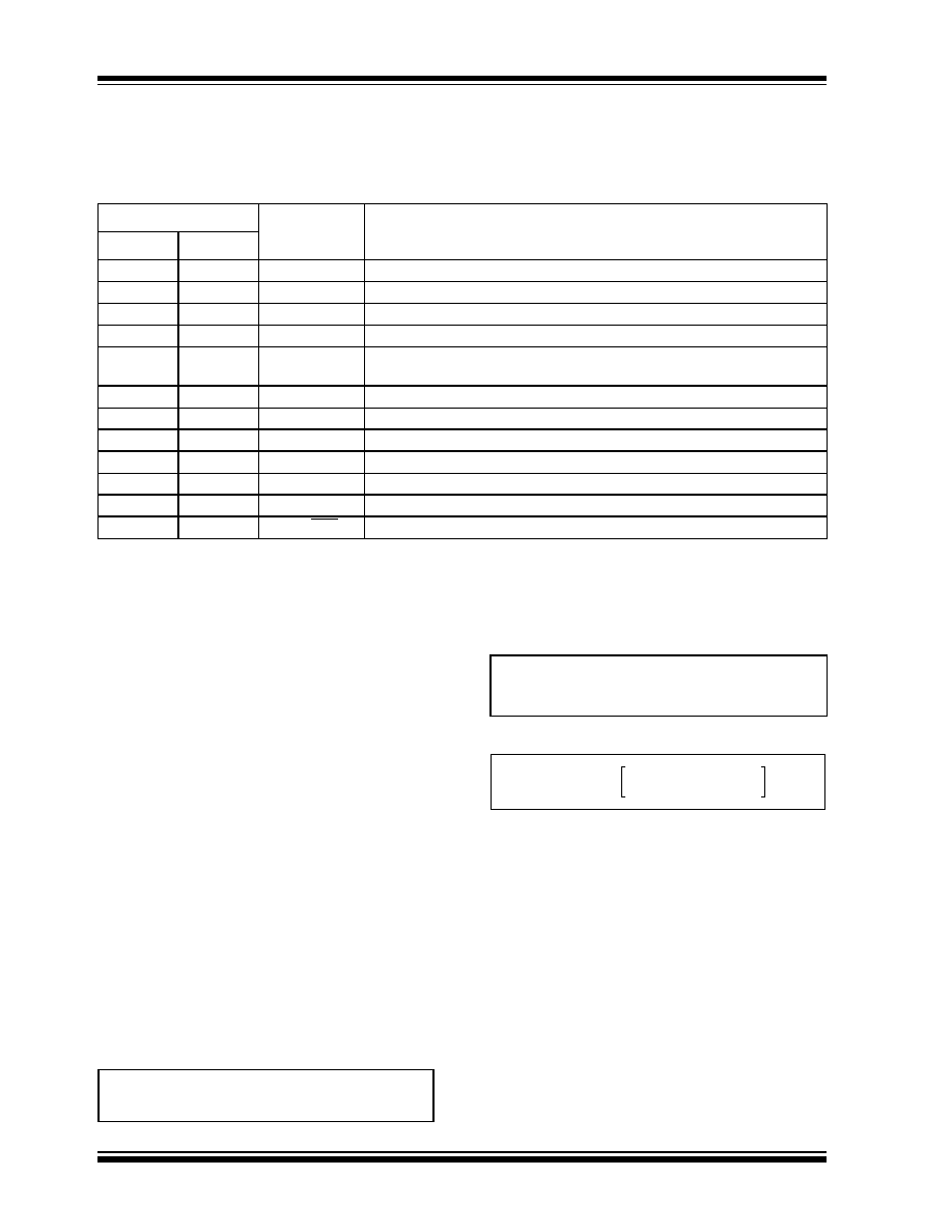
PIN DESCRIPTIONS
The descriptions of the pins are listed in Table 2-1.
TABLE 2-1:
PIN FUNCTION TABLE
3.0
DETAILED DESCRIPTION
3.1
Theory of Operation
Figure 3-1 shows the major elements of the TC7650.
There are two amplifiers (the main amplifier and the
nulling amplifier), and both have offset null capability.
The main amplifier is connected full-time from the input
to the output. The nulling amplifier, under the control of
the chopping frequency oscillator and clock circuit,
alternately nulls itself and the main amplifier. Two exter-
nal capacitors provide the required storage of the null-
ing potentials and the necessary nulling loop time
constants. The nulling arrangement operates over the
full common mode and power supply ranges, and is
also independent of the output level, thus giving excep-
tionally high CMRR, PSRR and A
VOL
.
Careful balancing of the input switches minimizes
chopper frequency charge injection at the input termi-
nals, and the feed forward type injection into the com-
pensation capacitor that can cause output spikes in this
type of circuit.
The circuit's offset voltage compensation is easily
shown. With the nulling inputs shorted, a voltage
almost identical to the nulling amplifier offset voltage is
stored on C
A
. The effective offset voltage at the null
amplifier input is:
EQUATION 3-1:
After the nulling amplifier is zeroed, the main amplifier
is zeroed; the A switches open and B switches close.
The output voltage equation is:
EQUATION 3-2:
EQUATION 3-3:
As desired, the device offset voltages are reduced by
the high open loop gain of the nulling amplifier.
3.2
Output Stage/Loading
The output circuit is a high impedance stage (approxi-
mately 18k
). With loads less than this, the chopper
amplifier behaves in some ways like a trans-conduc-
tance amplifier whose open-loop gain is proportional to
load resistance. For example, the open loop gain will
be 17dB lower with a 1k
load than with a 10k
load.
If the amplifier is used strictly for DC, the lower gain is
of little consequence, since the DC gain is typically
greater than 120dB, even with a 1k
load. In wideband
applications, the best frequency response will be
achieved with a load resistor of 10k
or higher. This
results in a smooth 6dB/octave response from 0.1Hz to
2MHz, with phase shifts of less than 10° in the transi-
Pin Number
Symbol
Description
8-pin DIP
14-pin DIP
1,8
2,1
C
A
, C
B
Nulling capacitor pins
2
4
-INPUT
Inverting Input
3
5
+INPUT
Non-inverting Input
4
7
V
SS
Negative Power Supply
5
9
OUTPUT
CLAMP
Output Voltage Clamp
6
10
OUTPUT
Output
7
11
V
DD
Positive Power Supply
--
3,6
NC
No internal connection
--
8
C
RETN
Capacitor current return pin
--
12
INT CLK OUT
Internal Clock Output
--
13
EXT CLK IN
External Clock Input
--
14
INT/EXT
Select Internal or External Clock
V
OSE
1
A
N
1
+
------------------V
OSN
=
V
OUT
= A
M
[
V
OSM
+ (V
+
- V
-
) + A
N
(V
+
- V
-
) + A
N
V
OSE
]
V
OUT
A
M
A
N
V
+
V
-
(
)
V
OSM
V
OSN
+
A
N
-------------------------------------------
+
=
©
2002 Microchip Technology Inc.
DS21463B-page 5
TC7650
tion region, where the main amplifier takes over from
the null amplifier. The clock frequency sets the transi-
tion region.
3.3
Intermodulation
Previous chopper stabilized amplifiers have suffered
from intermodulation effects between the chopper fre-
quency and input signals. These arise because the
finite AC gain of the amplifier results in a small AC sig-
nal at the input. This is seen by the zeroing circuit as an
error signal, which is chopped and fed back, thus inject-
ing sum and difference frequencies, and causing dis-
turbances to the gain and phase versus frequency
characteristics near the chopping frequency. These
effects are substantially reduced in the TC7650 by
feeding the nulling circuit with a dynamic current corre-
sponding to the compensation capacitor current in such
a way as to cancel that portion of the input signal due
to a finite AC gain. The intermodulation and gain/phase
disturbances are held to very low values, and can gen-
erally be ignored.
FIGURE 3-1:
TC7650 CONTAINS A NULLING AND MAIN AMPLIFIER. OFFSET CORRECTION
VOLTAGES ARE STORED ON TWO EXTERNAL CAPACITORS
.
FIGURE 3-2:
NULLING CAPACITOR
CONNECTION
3.4
Nulling Capacitor Connection
The offset voltage correction capacitors are connected
to C
A
and C
B
. The common capacitor connection is
made to V
SS
(Pin 4) on the 8-pin packages and to
capacitor return (C
RETN
, Pin 8) on the 14-pin packages.
The common connection should be made through a
separate PC trace or wire to avoid voltage drops. The
capacitors outside foil, if possible, should be connected
to C
RETN
or V
SS
.
3.5
Clock Operation
The internal oscillator is set for a 200Hz nominal chop-
ping frequency on both the 8- and 14-pin DIPs. With the
14-pin DIP TC7650, the 200 Hz internal chopping fre-
quency is available at the internal clock output (Pin 12).
A 400Hz nominal signal will be present at the external
clock input pin (Pin 13) with INT/EXT high or open. This
is the internal clock signal before a divide-by-two oper-
ation.
The 14-pin DIP device can be driven by an external
clock. The INT/EXT input (Pin 14) has an internal pull-
up and may be left open for internal clock operation. If
an external clock is used, INT/EXT must be tied to V
SS
(Pin 7) to disable the internal clock. The external clock
signal is applied to the external clock input (Pin 13).
The external clock amplitude should swing between
V
DD
and ground for power supplies up to ±6V and
between V
+
and V
+
-6V for higher supply voltages.
At low frequencies the external clock duty cycle is not
critical, since an internal divide-by-two gives the
desired 50% switching duty cycle. The offset storage
correction capacitors are charged only when the exter-
nal clock input is high. A 50% to 80% external clock
Null
Main
Amplifier
Null
Amplifier
Gain = A
M
B
A
B
A
+
C
B
C
A
TC7650
Null
-
+
V-
V+
Gain = A
N
, Offset = V
OSN
V
OUT
Analog Input
-
V
DD
V
SS
6
4
8
1
3
2
7
C
A
C
B
+
V
DD
TC7650
10
1
8
2
5
4
11
C
A
C
B
+
7
V
SS
14-PIN PACKAGE
8-PIN PACKAGE
TC7650
-
-
TC7650
DS21463B-page 6
©
2002 Microchip Technology Inc.
positive duty cycle is desired for frequencies above
500Hz to ensure transients settle before the internal
switches open.
The external clock input can also be used as a strobe
input. If a strobe signal is connected at the external
clock input so that it is LOW during the time an overload
signal is applied, neither capacitor will be charged. The
leakage currents at the capacitors pins are very low. At
25°C a typical TC7650 will drift less than 10
µ
V/sec.
3.6
Output Clamp
Chopper-stabilized systems can show long recovery
times from overloads. If the output is driven to either
supply rail, output saturation occurs. The inputs are no
longer held at a "virtual ground." The V
OS
null circuit
treats the differential signal as an offset and tries to cor-
rect it by charging the external capacitors. The nulling
circuit also saturates. Once the input signal returns to
normal, the response time is lengthened by the long
recovery time of the nulling amplifier and external
capacitors.
Through an external clamp connection, the TC7650
eliminates the overload recovery problem by reducing
the feedback network gain before the output voltage
reaches either supply rail.
FIGURE 3-3:
INTERNAL CLAMP CIRCUIT
FIGURE 3-4:
NON-INVERTING AMPLIFIER
WITH OPTIONAL CLAMP
FIGURE 3-5:
INVERTING AMPLIFIER WITH
OPTIONAL CLAMP
The output clamp circuit is shown in Figure 3-3, with
typical inverting and non-inverting circuit connections
shown in Figures 3-4 and 3-5. Output voltage versus
clamp circuit current characteristics are shown in the
typical operating curves. For the clamp to be fully effec-
tive, the impedance across the clamp output should be
greater than 100k
.
3.7
Latch-Up Avoidance
Junction-isolated CMOS circuits inherently include a
parasitic 4-layer (p-n-p-n) structure which has charac-
teristics similar to an SCR. Under certain circum-
stances this junction may be triggered into a low-
impedance state, resulting in excessive supply current.
To avoid this condition, no voltage greater than 0.3V
beyond the supply rails should be applied to any pin. In
general, the amplifier supplies must be established
either at the same time or before any input signals are
applied. If this is not possible, the drive circuits must
limit input current flow to under 0.1mA to avoid latch-
up.
3.8
Thermoelectric Potentials
Precision DC measurements are ultimately limited by
thermoelectric potentials developed in thermocouple
junctions of dissimilar metals, alloys, silicon, etc.
Unless all junctions are at the same temperature, ther-
moelectric voltages, typically around 0.1
µ
V/°C, but up
to tens of
µ
V/°C for some materials, will be generated.
In order to realize the benefits extremely-low offset volt-
ages provide, it is essential to take special precautions
to avoid temperature gradients. All components should
be enclosed to eliminate air movement, especially
those caused by power dissipating elements in the sys-
tem.
Low
thermoelectric
co-efficient
connections
should be used where possible and power supply volt-
ages and power dissipation should be kept to a mini-
mum. High impedance loads are preferable, and
separation from surrounding heat dissipating elements
is advised.
Internal
Positive Clamp Bias
V+ - V
T
V+ - 0.7
P-Channel
Output
Clamp Pin
N-Channel
TC7650
+
C
R
C
Output
Input
For Full Clamp Effect
R
2
R
1
R
3
+ (R1/R2) 100 k
0.1µF
Connect To V
SS
On 8-Pin DIP.
*
*
R
Clamp
3
TC7650
Clamp
+
C
R
C
R
1
Output
0.1 F
µ
0.1 F
µ
Input
R
2
For Full Clamp
Effect
*
Connect To V
R
On 8-Pin DIP.
*
(R
1
R
2
) 100 k
©
2002 Microchip Technology Inc.
DS21463B-page 7
TC7650
3.9
Pin Compatibility
On the 8-pin mini-DIP TC7650, the external null stor-
age capacitors are connected to pins 1 and 8. On most
other operational amplifiers these are left open or are
used for offset potentiometer or compensation capaci-
tor connections.
For OP05 and OP07 operational amplifiers, the
replacement of the offset null potentiometer between
pins 1 and 8 by two capacitors from the pins to V
SS
will
convert the OP05/07 pin configurations for TC7650
operation. For LM108 devices, the compensation
capacitor is replaced by the external nulling capacitors.
The LM101/748/709 pinouts are modified similarly by
removing any circuit connections to Pin 5. On the
TC7650, Pin 5 is the output clamp connection.
Other operational amplifiers may use this pin as an off-
set or compensation point.
The minor modifications needed to retrofit a TC7650
into existing sockets operating at reduced power sup-
ply voltages make prototyping and circuit verification
straightforward.
3.10
Input Guarding
High impedance, low leakage CMOS inputs allow the
TC7650 to make measurements of high-impedance
sources. Stray leakage paths can increase input cur-
rents and decrease input resistance unless inputs are
guarded. A guard is a conductive PC trace surrounding
the input terminals. The ring connects to a low imped-
ance point at the same potential as the inputs. Stray
leakages are absorbed by the low impedance ring. The
equal potential between ring and inputs prevents input
leakage currents. Typical guard connections are shown
in Figure 3-6.
The 14-pin DIP configuration has been specifically
designed to ease input guarding. The pins adjacent to
the inputs are unused.
In applications requiring low leakage currents, boards
should be cleaned thoroughly and blown dry after sol-
dering. Protective coatings will prevent future board
contamination.
3.11
Component Selection
The two required capacitors, C
A
and C
B
, have optimum
values, depending on the clock or chopping frequency.
For the preset internal clock, the correct value is 0.1
µ
F.
To maintain the same relationship between the chop-
ping frequency and the nulling time constant, the
capacitor values should be scaled in proportion to the
external clock, if used. High quality film type capacitors
(such as Mylar) are preferred; ceramic or other lower
grade capacitors may be suitable in some applications.
For fast settling on initial turn-on, low dielectric absorp-
tion capacitors (such as polypropylene) should be
used. With ceramic capacitors, several seconds may
be required to settle to 1
µ
V.
FIGURE 3-6:
INPUT GUARD CONNECTION
Input
+
Output
R
2
Inverting Amplifier
Input
+
Output
Follower
Input
+
Output
R
2
R
1
Noninverting Amplifier
R
3
*
R
3
*
Should Be Low
Impedence For
Optimum Guarding
NOTE: R
3
=
R
1
R
2
R
1
+ R
2
R
3
*
R
1
-
-
-
TC7650
DS21463B-page 8
©
2002 Microchip Technology Inc.
4.0
TYPICAL CHARACTERISTICS
Note:
The graphs and tables provided following this note are a statistical summary based on a limited number of
samples and are provided for informational purposes only. The performance characteristics listed herein
are not tested or guaranteed. In some graphs or tables, the data presented may be outside the specified
operating range (e.g., outside specified power supply range) and therefore outside the warranted range.
4.0 4.1 4.2 4.3 4.4 4.5 4.6 4.7 4.8 4.9 5.0
OUTPUT VOLTAGE (V)
Positive Clamp Current
vs. Output Voltage
CLAMP CURRENT
1 mA
0.1 mA
0.01 mA
1 A
m
0.1 A
0.01 A
m
1 nA
1 pA
0.01 nA
0.1 nA
m
-4.0 -4.1 -4.2 -4.3 -4.4 -4.5 -4.6 -4.7 -4.8 -4.9 -5.0
OUTPUT VOLTAGE (V)
Negative Clamp Current
vs. Output Voltage
CLAMP CURRENT
3.0
2.6
2.2
1.8
1.0
1.4
5
6
7
8
9
10 11 12
13 14 15
SUPPLY VOLTAGE (V)
Supply Current vs.
Supply Voltage
SUPPL
Y CURRENT (mA)
Gain/Phase vs. Frequency
30
20
10
0
10
20
30
40
50
60
1k
10k
100k
1M
10M
GAIN (dB)
225
180
135
90
45
0
-45
-90
-135
-180
FREQUENCY (H )
z
PHASE
(
de
g)
1 mA
0.1 mA
0.01 mA
1 A
m
0.1 A
0.01 A
m
1 nA
1 pA
0.01 nA
0.1 nA
m
CLOSED-LOOP
GAIN = 20
PHASE
GAIN
T
A
= +25°C
V
S
= ±5V
T
A
= +25°C
V
S
= ±5V
T
A
= +25°C
©
2002 Microchip Technology Inc.
DS21463B-page 9
TC7650
5.0
PACKAGING INFORMATION
5.1
Package Marking Information
Package marking information not available at this time.
5.2
Package Dimensions
3
°
MIN.
PIN 1
.260 (6.60)
.240 (6.10)
.045 (1.14)
.030 (0.76)
.070 (1.78)
.040 (1.02)
.400 (10.16)
.348 (8.84)
.200 (5.08)
.140 (3.56)
.150 (3.81)
.115 (2.92)
.110 (2.79)
.090 (2.29)
.022 (0.56)
.015 (0.38)
.040 (1.02)
.020 (0.51)
.015 (0.38)
.008 (0.20)
.310 (7.87)
.290 (7.37)
.400 (10.16)
.310 (7.87)
8-Pin Plastic DIP
Dimensions: inches (mm)
.260 (6.60)
.240 (6.10)
.770 (19.56)
.745 (18.92)
.310 (7.87)
.290 (7.37)
.040 (1.02)
.020 (0.51)
.070 (1.78)
.045 (1.14)
.022 (0.56)
.015 (0.38)
.110 (2.79)
.090 (2.29)
.200 (5.08)
.140 (3.56)
.150 (3.81)
.115 (2.92)
PIN 1
14-Pin PDIP (Narrow)
.015 (0.38)
.008 (0.20)
3
°
MIN.
.400 (10.16)
.310 (7.87)
Dimensions: inches (mm)

TC7650
DS21463B-page 10
©
2002 Microchip Technology Inc.

©
2002 Microchip Technology Inc.
DS21463B-page 11
TC7650
SALES AND SUPPORT
Data Sheets
Products supported by a preliminary Data Sheet may have an errata sheet describing minor operational differences
and recommended workarounds. To determine if an errata sheet exists for a particular device, please contact one of
the following:
1.
Your local Microchip sales office
2.
The Microchip Corporate Literature Center U.S. FAX: (480) 792-7277
3.
The Microchip Worldwide Site (www.microchip.com)
Please specify which device, revision of silicon and Data Sheet (include Literature #) you are using.
New Customer Notification System
Register on our web site (www.microchip.com/cn) to receive the most current information on our products.

TC7650
DS21463B-page 12
©
2002 Microchip Technology Inc.
NOTES:
2002 Microchip Technology Inc.
DS21463B - page 13
Information contained in this publication regarding device
applications and the like is intended through suggestion only
and may be superseded by updates. It is your responsibility to
ensure that your application meets with your specifications.
No representation or warranty is given and no liability is
assumed by Microchip Technology Incorporated with respect
to the accuracy or use of such information, or infringement of
patents or other intellectual property rights arising from such
use or otherwise. Use of Microchip's products as critical com-
ponents in life support systems is not authorized except with
express written approval by Microchip. No licenses are con-
veyed, implicitly or otherwise, under any intellectual property
rights.
Trademarks
The Microchip name and logo, the Microchip logo, FilterLab,
K
EE
L
OQ
, microID,
MPLAB, PIC, PICmicro, PICMASTER,
PICSTART, PRO MATE, SEEVAL and The Embedded Control
Solutions Company are registered trademarks of Microchip Tech-
nology Incorporated in the U.S.A. and other countries.
dsPIC, ECONOMONITOR, FanSense, FlexROM, fuzzyLAB,
In-Circuit Serial Programming, ICSP, ICEPIC, microPort,
Migratable Memory, MPASM, MPLIB, MPLINK, MPSIM,
MXDEV, PICC, PICDEM, PICDEM.net, rfPIC, Select Mode
and Total Endurance are trademarks of Microchip Technology
Incorporated in the U.S.A.
Serialized Quick Turn Programming (SQTP) is a service mark
of Microchip Technology Incorporated in the U.S.A.
All other trademarks mentioned herein are property of their
respective companies.
© 2002, Microchip Technology Incorporated, Printed in the
U.S.A., All Rights Reserved.
Printed on recycled paper.
Microchip received QS-9000 quality system
certification for its worldwide headquarters,
design and wafer fabrication facilities in
Chandler and Tempe, Arizona in July 1999
and Mountain View, California in March 2002.
The Company's quality system processes and
procedures are QS-9000 compliant for its
PICmicro
®
8-bit MCUs, K
EE
L
OQ
®
code hopping
devices, Serial EEPROMs, microperipherals,
non-volatile memory and analog products. In
addition, Microchip's quality system for the
design and manufacture of development
systems is ISO 9001 certified.

DS21463B-page 14
©
2002 Microchip Technology Inc.
AMERICAS
Corporate Office
2355 West Chandler Blvd.
Chandler, AZ 85224-6199
Tel: 480-792-7200 Fax: 480-792-7277
Technical Support: 480-792-7627
Web Address: http://www.microchip.com
Rocky Mountain
2355 West Chandler Blvd.
Chandler, AZ 85224-6199
Tel: 480-792-7966 Fax: 480-792-7456
Atlanta
500 Sugar Mill Road, Suite 200B
Atlanta, GA 30350
Tel: 770-640-0034 Fax: 770-640-0307
Boston
2 Lan Drive, Suite 120
Westford, MA 01886
Tel: 978-692-3848 Fax: 978-692-3821
Chicago
333 Pierce Road, Suite 180
Itasca, IL 60143
Tel: 630-285-0071 Fax: 630-285-0075
Dallas
4570 Westgrove Drive, Suite 160
Addison, TX 75001
Tel: 972-818-7423 Fax: 972-818-2924
Detroit
Tri-Atria Office Building
32255 Northwestern Highway, Suite 190
Farmington Hills, MI 48334
Tel: 248-538-2250 Fax: 248-538-2260
Kokomo
2767 S. Albright Road
Kokomo, Indiana 46902
Tel: 765-864-8360 Fax: 765-864-8387
Los Angeles
18201 Von Karman, Suite 1090
Irvine, CA 92612
Tel: 949-263-1888 Fax: 949-263-1338
New York
150 Motor Parkway, Suite 202
Hauppauge, NY 11788
Tel: 631-273-5305 Fax: 631-273-5335
San Jose
Microchip Technology Inc.
2107 North First Street, Suite 590
San Jose, CA 95131
Tel: 408-436-7950 Fax: 408-436-7955
Toronto
6285 Northam Drive, Suite 108
Mississauga, Ontario L4V 1X5, Canada
Tel: 905-673-0699 Fax: 905-673-6509
ASIA/PACIFIC
Australia
Microchip Technology Australia Pty Ltd
Suite 22, 41 Rawson Street
Epping 2121, NSW
Australia
Tel: 61-2-9868-6733 Fax: 61-2-9868-6755
China - Beijing
Microchip Technology Consulting (Shanghai)
Co., Ltd., Beijing Liaison Office
Unit 915
Bei Hai Wan Tai Bldg.
No. 6 Chaoyangmen Beidajie
Beijing, 100027, No. China
Tel: 86-10-85282100 Fax: 86-10-85282104
China - Chengdu
Microchip Technology Consulting (Shanghai)
Co., Ltd., Chengdu Liaison Office
Rm. 2401, 24th Floor,
Ming Xing Financial Tower
No. 88 TIDU Street
Chengdu 610016, China
Tel: 86-28-6766200 Fax: 86-28-6766599
China - Fuzhou
Microchip Technology Consulting (Shanghai)
Co., Ltd., Fuzhou Liaison Office
Unit 28F, World Trade Plaza
No. 71 Wusi Road
Fuzhou 350001, China
Tel: 86-591-7503506 Fax: 86-591-7503521
China - Shanghai
Microchip Technology Consulting (Shanghai)
Co., Ltd.
Room 701, Bldg. B
Far East International Plaza
No. 317 Xian Xia Road
Shanghai, 200051
Tel: 86-21-6275-5700 Fax: 86-21-6275-5060
China - Shenzhen
Microchip Technology Consulting (Shanghai)
Co., Ltd., Shenzhen Liaison Office
Rm. 1315, 13/F, Shenzhen Kerry Centre,
Renminnan Lu
Shenzhen 518001, China
Tel: 86-755-2350361 Fax: 86-755-2366086
Hong Kong
Microchip Technology Hongkong Ltd.
Unit 901-6, Tower 2, Metroplaza
223 Hing Fong Road
Kwai Fong, N.T., Hong Kong
Tel: 852-2401-1200 Fax: 852-2401-3431
India
Microchip Technology Inc.
India Liaison Office
Divyasree Chambers
1 Floor, Wing A (A3/A4)
No. 11, O'Shaugnessey Road
Bangalore, 560 025, India
Tel: 91-80-2290061 Fax: 91-80-2290062
Japan
Microchip Technology Japan K.K.
Benex S-1 6F
3-18-20, Shinyokohama
Kohoku-Ku, Yokohama-shi
Kanagawa, 222-0033, Japan
Tel: 81-45-471- 6166 Fax: 81-45-471-6122
Korea
Microchip Technology Korea
168-1, Youngbo Bldg. 3 Floor
Samsung-Dong, Kangnam-Ku
Seoul, Korea 135-882
Tel: 82-2-554-7200 Fax: 82-2-558-5934
Singapore
Microchip Technology Singapore Pte Ltd.
200 Middle Road
#07-02 Prime Centre
Singapore, 188980
Tel: 65-6334-8870 Fax: 65-6334-8850
Taiwan
Microchip Technology Taiwan
11F-3, No. 207
Tung Hua North Road
Taipei, 105, Taiwan
Tel: 886-2-2717-7175 Fax: 886-2-2545-0139
EUROPE
Denmark
Microchip Technology Nordic ApS
Regus Business Centre
Lautrup hoj 1-3
Ballerup DK-2750 Denmark
Tel: 45 4420 9895 Fax: 45 4420 9910
France
Microchip Technology SARL
Parc d'Activite du Moulin de Massy
43 Rue du Saule Trapu
Batiment A - ler Etage
91300 Massy, France
Tel: 33-1-69-53-63-20 Fax: 33-1-69-30-90-79
Germany
Microchip Technology GmbH
Gustav-Heinemann Ring 125
D-81739 Munich, Germany
Tel: 49-89-627-144 0 Fax: 49-89-627-144-44
Italy
Microchip Technology SRL
Centro Direzionale Colleoni
Palazzo Taurus 1 V. Le Colleoni 1
20041 Agrate Brianza
Milan, Italy
Tel: 39-039-65791-1 Fax: 39-039-6899883
United Kingdom
Arizona Microchip Technology Ltd.
505 Eskdale Road
Winnersh Triangle
Wokingham
Berkshire, England RG41 5TU
Tel: 44 118 921 5869 Fax: 44-118 921-5820
03/01/02
W
ORLDWIDE
S
ALES
AND
S
ERVICE