 | ÐлекÑÑоннÑй компоненÑ: TC7652CPD | СкаÑаÑÑ:  PDF PDF  ZIP ZIP |
Äîêóìåíòàöèÿ è îïèñàíèÿ www.docs.chipfind.ru
©
2002 Microchip Technology Inc.
DS21464B-page 1
Features
· Low Offset Over Temperature Range: 10
µ
V
· Ultra Low Long Term Drift: 150nV/Month
· Low Temperature Drift: 100nV/
°
C
· Low DC Input Bias Current: 15pA
· High Gain, CMRR and PSRR: 110dB Min
· Low Input Noise Voltage: 0.2
µ
V
p-p
(DC to 1Hz)
· Internally Compensated for Unity Gain Operation
· Clamp Circuit for Fast Overload Recovery
Applications
· Instrumentation
· Medical Instrumentation
· Embedded Control
· Temperature Sensor Amplifier
· Strain Gage Amplifier
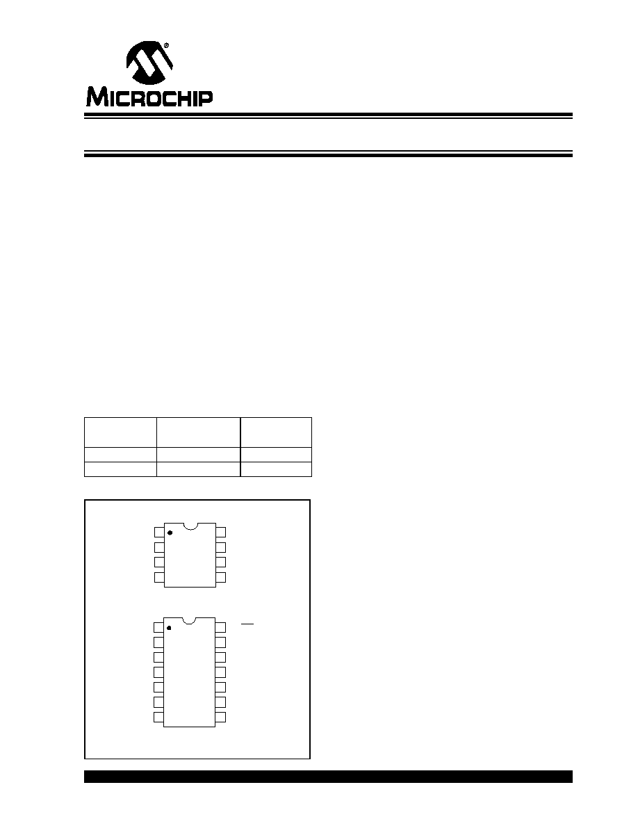
Device Selection Table
Package Type
General Description
The TC7652 is a lower noise version of the TC7650,
sacrificing some input specifications (bias current and
bandwidth) to achieve a 10x reduction in noise. All the
other benefits of the chopper technique are present,
(i.e, freedom from offset adjust, drift and reliability prob-
lems from external trim components). Like the TC7650,
the TC7652 requires only two noncritical external caps
for storing the chopped null potentials. There are no
significant chopping spikes, internal effects or over-
range lockup problems.
Part Number
Package
Temperature
Range
TC7652CPA
8-Pin Plastic DIP
0°C to +70°C
TC7652CPD
14-Pin Plastic DIP
0°C to +70°C
1
2
3
4
8
7
6
5
C
A
Output
TC7652CPA
-Input
+Input
V
SS
V
DD
C
B
Output
Clamp
V
SS
V
DD
1
2
3
4
5
6
7
14
13
12
11
10
9
8
NC
NC = No Internal Connection
(May Be Used As Input Guard)
INT/EXT
EXT CLK
In
INT CLK
Out
Output
Output
Clamp
C
RETN
-Input
+Input
NC
TC7652CPD
C
B
C
A
8-Pin DIP
14-Pin DIP
TC7652
Low Noise, Chopper Stabilized Operational Amplifier
TC7652
DS21464B-page 2
©
2002 Microchip Technology Inc.
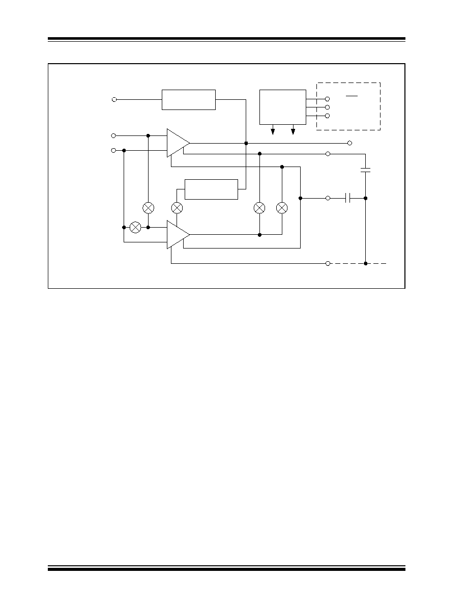
Functional Block Diagram
TC7652
NULL
NULL
Output
B
B
A
C
A
C
B
C
RETN
(1)
NULL
Amplifier
Main
Amplifier
Output Clamp
Circuit
Intermod
Comparator
Oscillator
B
A
INT/EXT
EXT CLK IN
CLK OUT
14-Pin DIP Only
B
A
Inputs
Output Clamp
(Not On "Z" Pinout)
NOTE 1: For 8-pin DIP connect to V
SS
, or to C
RET
on "Z" pinout.
V
SS
©
2002 Microchip Technology Inc.
DS21464B-page 3
TC7652
1.0
ELECTRICAL
CHARACTERISTICS
ABSOLUTE MAXIMUM RATINGS*
Total Supply Voltage (V
DD
to V
SS
) .......................+18V
Input Voltage .................... (V
DD
+0.3V) to (V
SS
0.3V)
Voltage on Oscillator Control Pins...............V
DD
to V
SS
Duration of Output Short Circuit ..................... Indefinite
Current Into Any Pin............................................ 10mA
While Operating (Note 1)............................ 100
µ
A
Package Power Dissipation (T
A
< 70°C
)
8-Pin Plastic DIP ....................................... 730mW
14-Pin Plastic DIP ..................................... 800mW
Storage Temperature Range .............. -65°C to +150°C
Operating Temperature Range
C Device .......................................... 0°C to +70°C
I Device ......................................... -25°C to +85°C
*Stresses above those listed under "Absolute Maximum
Ratings" may cause permanent damage to the device.
These are stress ratings only and functional operation of the
device at these or any other conditions above those indi-
cated in the operation sections of the specifications is not
implied. Exposure to Absolute Maximum Rating conditions
for extended periods my affect device reliability.
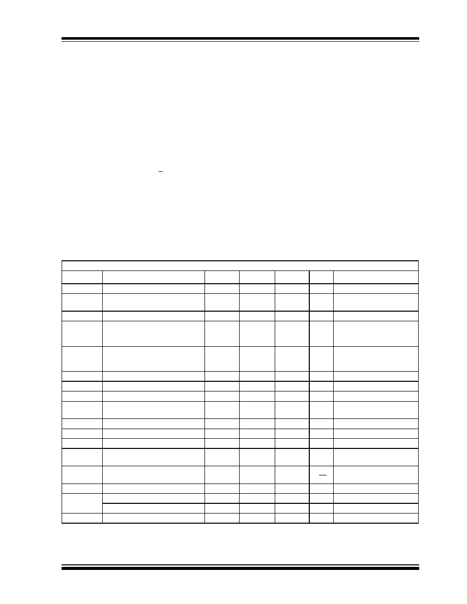
TC7652 ELECTRICAL SPECIFICATIONS
Electrical Characteristics: V
DD
= +5V, V
SS
= -5V, T
A
= +25°C, unless otherwise indicated.
Symbol
Parameter
Min
Typ
Max
Units
Test Conditions
V
OS
Input Offset Voltage
--
±2
±5
µ
V
T
A
= +25°C
TCV
OS
Average Temperature Co-efficient of
Input Offset Voltage
--
0.01
0.05
µ
V/°C
0°C < T
A
< +70°C
V
OS
/DT
Offset Voltage vs Time
--
150
--
nV/mo
I
BIAS
Input Bias Current (CLK On)
--
--
--
30
100
250
100
--
1000
pA
T
A
= +25°C
0°C < T
A
< +70°C
-25°C < T
A
< +85°C
I
BIAS
Input Bias Current (CLK Off)
--
--
--
15
35
100
30
--
1000
pA
T
A
= +25°C
0°C < T
A
< +70°C
-25°C < T
A
< +85°C
I
OS
Input Offset Current
--
25
150
pA
R
IN
Input Resistance
--
10
12
--
OL
Large Signal Voltage Gain
120
150
--
dB
R
L
= 10k
, V
OUT
= ±4V
V
OUT
Output Voltage Swing
(Note 2)
±4.7
--
±4.85
±4.95
--
--
V
R
L
= 10k
R
L
= 100k
CMVR
Common Mode Voltage Range
-4.3
--
+3.5
V
MRR
Common Mode Rejection Ratio
120
140
--
dB
CMVR = -4.3V to +3.5V
PSRR
Power Supply
120
140
--
dB
±3V to ±8V
e
N
Input Noise Voltage
--
--
0.2
0.7
1.5
5
µ
V
P-P
µ
V
P-P
R
S
= 100
, DC to 1Hz
DC to 10Hz
I
N
Input Noise Current
--
0.01
--
pA/
Hz
f
= 10Hz
GBW
Unity Gain Bandwidth
--
0.4
--
MHz
SR
Slew Rate
--
1
--
V/
µ
sec C
L
= 50pF, R
L
= 10k
Overshoot
--
15
--
%
V
DD
, V
SS
Operating Supply Range
5
--
16
V
Note
1:
Limiting input current to 100
µ
A is recommended to avoid latch-up problems. Typically 1mA is safe however, this is not
guaranteed.
2:
Output clamp not connected. See typical characteristics curves for output swing versus clamp current characteristics.
3:
See "Output Clamp" under detailed description.
TC7652
DS21464B-page 4
©
2002 Microchip Technology Inc.
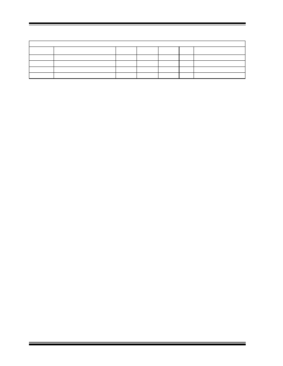
I
S
Supply Current
--
1
3
mA
No Load
f
CH
Internal Chopping Frequency
100
275
--
Hz
Pins 12 14 Open (DIP)
Clamp ON Current (Note 3)
25
100
--
µ
A
R
L
= 100k
Clamp OFF Current (Note 3)
--
1
--
pA
-4V
V
OUT
< +10V
TC7652 ELECTRICAL SPECIFICATIONS
(CONTINUED)
Electrical Characteristics: V
DD
= +5V, V
SS
= -5V, T
A
= +25°C, unless otherwise indicated.
Symbol
Parameter
Min
Typ
Max
Units
Test Conditions
Note
1:
Limiting input current to 100
µ
A is recommended to avoid latch-up problems. Typically 1mA is safe however, this is not
guaranteed.
2:
Output clamp not connected. See typical characteristics curves for output swing versus clamp current characteristics.
3:
See "Output Clamp" under detailed description.
©
2002 Microchip Technology Inc.
DS21464B-page 5
TC7652
2.0
PIN DESCRIPTIONS
The descriptions of the pins are listed in Table 2-1.
TABLE 2-1:
PIN FUNCTION TABLE
Pin Number
Symbol
Description
8-pin DIP
14-pin DIP
1,8
2,1
C
A
, C
B
Nulling capacitor pins
2
4
-INPUT
Inverting Input
3
5
+INPUT
Non-inverting Input
4
7
V
SS
Negative Power Supply
5
9
OUTPUT
CLAMP
Output Voltage Clamp
6
10
OUTPUT
Output
7
11
V
DD
Positive Power Supply
--
3,6
NC
No internal connection
--
8
C
RETN
Capacitor current return pin
--
12
INT CLK OUT
Internal Clock Output
--
13
EXT CLK IN
External Clock Input
--
14
INT/EXT
Select Internal or External Clock
TC7652
DS21464B-page 6
©
2002 Microchip Technology Inc.
3.0
DETAILED DESCRIPTION
3.1
Capacitor Connection
Connect the null storage capacitors to the C
A
and C
B
pins with a common connection to the C
RET
pin (14-pin
TC7652) or to V
SS
(8-pin TC7652). When connecting to
V
SS
, avoid injecting load current IR drops into the
capacitive circuitry by making this connection directly
via a separate wire or PC trace.
3.2
Output Clamp
In chopper stabilized amplifiers, the output clamp pin
reduces overload recovery time. When a connection is
made to the inverting input pin (summing junction), a
current path is created between that point and the out-
put pin, just before the device output saturates. This
prevents uncontrolled differential input voltages and
charge build-up on correction storage capacitors. Out-
put swing is reduced.
3.3
Clock
The TC7652 has a 550Hz internal oscillator, which is
divided by two before clocking the input chopper
switches. The 275Hz chopping frequency is available
at INT CLK OUT (Pin 12) on 14-pin devices. In normal
operation, INT/EXT (Pin 14), which has an internal pull-
up, can be left open.
An external clock can also be used. To disable the
internal clock and use an external one, the INT/EXT pin
must be tied to V
SS
. The external clock signal is then
applied to the EXT CLK IN input (Pin 13). An internal
divide-by-two provides a 50% switching duty cycle. The
capacitors are only charged when EXT CLK IN is high,
so a 50% to 80% positive duty cycle is recommended
for higher clock frequencies. The external clock can
swing between V
DD
and V
SS
, with the logic threshold
about 2.5V below V
DD
.
The output of the internal oscillator, before the divide-
by-two circuit, is available at EXT CLK IN when INT/
EXT is high or unconnected. This output can serve as
the clock input for a second TC7652 (operating in a
master/slave mode), so that both op amps will clock at
the same frequency. This prevents clock intermodula-
tion effects when two TC7652's are used in a differen-
tial amplifier configuration.
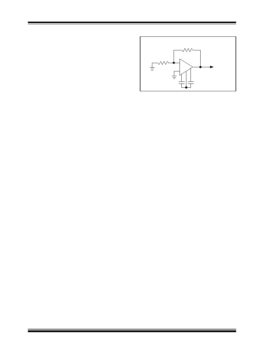
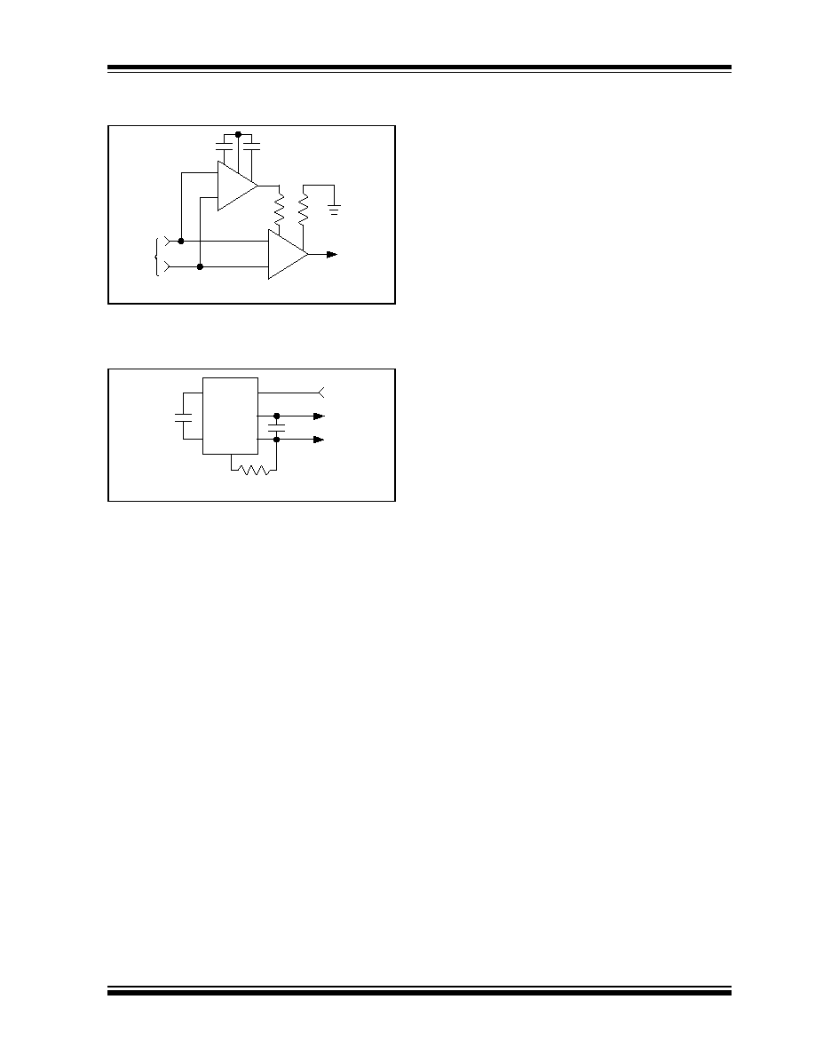
FIGURE 3-1:
TEST CIRCUIT
If the TC7652's output saturates, error voltages on the
external capacitors will slow overload recovery. This
condition can be avoided if a strobe signal is available.
The strobe signal is applied to EXT CLK IN and the
overload signal is applied to the amplifier while the
strobe is LOW. In this case, neither capacitor will be
charged. The low leakage of the capacitor pins allow
long measurements to be made within eligible errors
(typical capacitor drift is 10
µ
V/sec).
4.0
TYPICAL APPLICATIONS
4.1
Component Selection
C
A
and C
B
(external capacitors)should be in the 0.1
µ
F
to 1
µ
F range. For minimum clock ripple noise, use a
1
µ
F capacitor in broad bandwidth circuits. For limited
bandwidth applications where clock ripple is filtered
out, use a 0.1
µ
F capacitor for slightly lower offset volt-
age. High quality, film type capacitors (polyester or
polypropylene) are recommended, although a lower
grade ceramic may work in some applications. For
quickest settling after initial turn-on, use low dielectric
absorption
capacitors
(e.g.,
polypropylene).
With
ceramic capacitors, settling to 1
µ
V takes several sec-
onds.
4.2
Static Protection
Although input diodes static protect all device pins,
avoid strong electrostatic fields and discharges that
can cause degraded diode junction characteristics and
produce increased input-leakage currents.
+
-
Output
R2
R
1
0.1µF
0.1µF
TC7652
C
R
C
1k
1M
©
2002 Microchip Technology Inc.
DS21464B-page 7
TC7652
4.3
Output Stage/Load Driving
The output circuit is high impedance (about 18k
).
With lesser loads, the chopper amplifier behaves
somewhat like a transconductance amplifier with an
open-loop gain proportional to load resistance. (For
example, the open-loop gain is 17dB lower with a 1k
.
load than with a 10k
load.) If the amp is used only for
DC, the DC gain is typically greater than 120dB (even
with a 1k
load), and this lower gain is inconsequential.
For wide band, the best frequency response occurs
with a load resistor of at least 10k
. This produces a
6dB/octave response from 0.1Hz to 2MHz, with phase
shifts of less than 2 degrees in the transition region,
where the main amplifier takes over from the null ampli-
fier.
FIGURE 4-1:
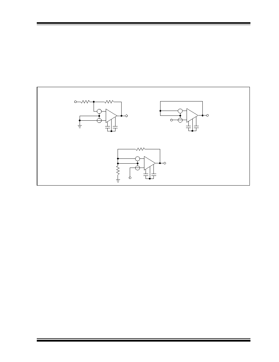
CONNECTION OF INPUT GUARDS
4.4
Thermoelectric Effects
The thermoelectric (Seebeck) effects in thermocouple
junctions of dissimilar metals, alloys, silicon, etc. limit
ultra high precision DC amplifiers. Unless all junctions
are at the same temperature, thermoelectric voltages
around 0.1
µ
V/
°
C (up to tens of
µ
V/
°
C for some materi-
als) are generated. To realize the low offset voltages of
the chopper, avoid temperature gradients. Enclose
components to eliminate air movement, especially from
power dissipating elements in the system. Where pos-
sible, use low thermoelectric co-efficient connections.
Keep power supply voltages and power dissipation to a
minimum. Use high impedance loads and seek maxi-
mum separation from surrounding heat disipating ele-
ments.
4.5
Guarding
To benefit from TC7652 low input currents, take care
assembling printed circuit boards. Clean boards with
alcohol or TCE and blow dry with compressed air. To
prevent contamination, coat boards with epoxy or sili-
cone rubber.
Even if boards are cleaned and coated, leakage cur-
rents may occur because input pins are next to pins at
supply potentials. To reduce this leakage, use guarding
to lower the voltage difference between the inputs and
adjacent metal runs. The guard (a conductive ring sur-
rounding inputs) is connected to a low impedance point
at about the same voltage as inputs. The guard
absorbs leakage currents from high voltage pins.
The 14-pin dual-in-line arrangement simplifies guard-
ing. Like the LM108 pin configuration (but unlike the
101A and 741), pins next to inputs are not used.
Input
+
Output
R
2
R
1
Inverting Amplifier
Input
+
Output
Follower
Input
+
Output
R
2
R
1
Noninverting Amplifier
TC7652
TC7652
TC7652
-
-
-
TC7652
DS21464B-page 8
©
2002 Microchip Technology Inc.
4.6
Pin Compatibility
Where possible, the 8-pin device pinout conforms to
such industry standards as the LM101 and LM741. Null
storing external capacitors connect to Pins 1 and 8,
which are usually for offset null or compensation capac-
itors. Output clamp (Pin 5) is similarly used. For OP05
and OP07 devices, replacement of the offset null
potentiometer (connected between Pins 1 and 8 and
V
DD
by two capacitors from those pins to V
SS
) provides
compatibility. Replacing the compensation capacitor
between Pins 1 and 8 by two capacitors to V
SS
is
required. The same operation (with the removal of any
connection to Pin 5) works for LM101,
µ
A748 and sim-
ilar parts.
Because NC pins provide guarding between input and
other pins, the 14-pin device pinout conforms closely to
the LM108. Because this device does not use any extra
pins and does not provide offset nulling (but requires a
compensation capacitor), some layout changes are
necessary to convert to the TC7652.
4.7
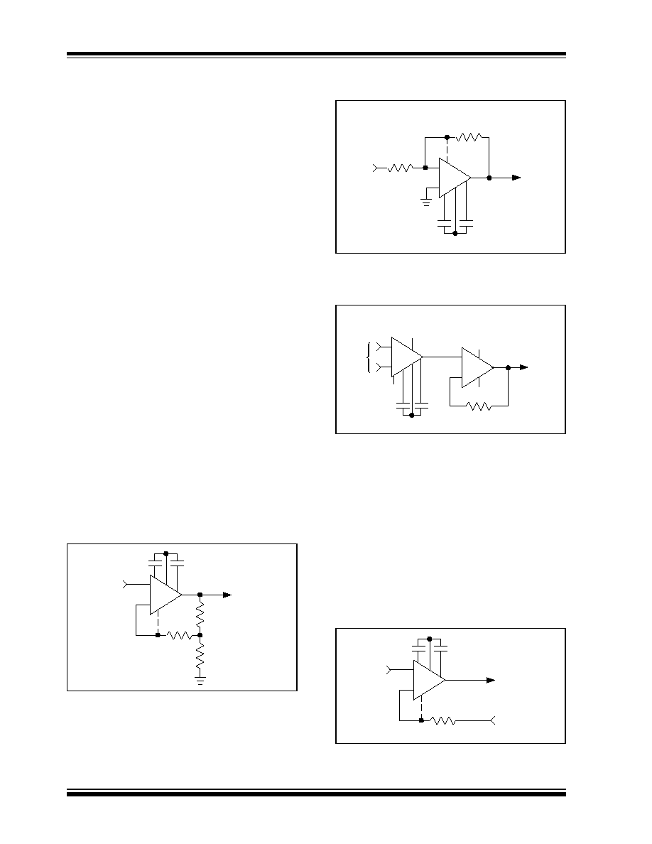
Some Applications
Figures 4-2 and 4-3 show basic inverting and nonin-
verting amplifier circuits using the output clamping cir-
cuit to enhance overload recovery performance. The
only limitations on replacing other op amps with the
TC7652 are supply voltage (±8V maximum) and output
drive capability (10k
load for full swing). Overcome
these limitations with a booster circuit (Figure 4-4) to
combine output capabilities of the LM741 (or other
standard device) with input capabilities of the TC7652.
These two form a composite device, therefore, when
adding the feedback network, the monitor loop gains
stability.
FIGURE 4-2:
NONINVERTING
AMPLIFIER WITH
OPTIONAL CLAMP
FIGURE 4-3:
INVERTING AMPLIFIER
WITH OPTIONAL CLAMP
FIGURE 4-4:
USING 741 TO BOOST
OUTPUT DRIVE
CAPABILITY
Figure 4-5 shows the clamp circuit of a zero offset com-
parator. Because the clamp circuit requires the invert-
ing input to follow the input signal, problems with a
chopper stabilized op amp are avoided. The threshold
input must tolerate the output clamp current
V
IN
/R
without disrupting other parts of the system.
Figure 4-6 shows how the TC7652 can offset null high
slew rate and wideband amplifiers.
Mixing the TC7652 with circuits operating at ±15V
requires a lower supply voltage divider with the TC7660
voltage converter circuit operated "backwards." Figure
4-7 shows an approximate connection.
FIGURE 4-5:
LOW OFFSET
COMPARATOR
TC7652
+
Output
Clamp
Input
0.1µF
R
2
R
1
R
3
0.1µF
+
Output
Input
R
2
R
1
Clamp
0.1µF
0.1µF
TC7652
+
+
+15V
-15V
-7.5V
0.1
µF
In
Out
-7.5V
0.1
µF
10k
TC7652
741
TC7652
+
V
OUT
Clamp
V
IN
0.1µF
0.1µF
200k
to 2m
V
TH
©
2002 Microchip Technology Inc.
DS21464B-page 9
TC7652
FIGURE 4-6:
1437 OFFSET NULLED BY
TC7652
FIGURE 4-7:
SPLITTING +15V WITH
THE 7660 AT >95%
EFFICIENCY
+
TC7652
Out
In
+
22k
22k
Fast
Amplifier
2
4
5
3
8
TC7660
6
10µF
1MW
10µF
+15V
+7.5V
0V
TC7652
DS21464B-page 10
©
2002 Microchip Technology Inc.
5.0
TYPICAL CHARACTERISTICS
Note:
The graphs and tables provided following this note are a statistical summary based on a limited number of
samples and are provided for informational purposes only. The performance characteristics listed herein
are not tested or guaranteed. In some graphs or tables, the data presented may be outside the specified
operating range (e.g., outside specified power supply range) and therefore outside the warranted range.
2
3
4
5
6
7
8
± SUPPLY VOLTAGE (V)
1400
1200
1000
800
600
400
200
0
SUPPLY CURRENT (µA)
Supply Current
vs ± Supply Voltage
OUTPUT VOLTAGE (V)
4.0 4.1 4.2 4.3 4.4 4.5 4.6 4.7 4.8 4.9 5.0
1 mA
0.1mA
0.01mA
1µA
0.1µA
0.01µA
1nA
0.1nA
0.01nA
1pA
CLAMP CURRENT
Positive Clamp Current
SOURCE
SINK
Output Resistance
vs Output Voltage
100
OUTPUT RESISTANCE (W)
-3.0
OUTPUT VOLTAGE (V)
1k
10k
100k
1M
-5.0
-4.0
1 sec/DIV
2 µV/DIV
Noise at 0.1Hz to 10Hz
OUTPUT VOLTAGE (V)
4.0 4.1 4.2 4.3 4.4 4.5 4.6 4.7 4.8 4.9 5.0
1mA
0.1mA
0.01mA
1µA
0.1µA
0.01µA
1nA
0.1nA
0.01nA
1pA
CLAMP CURRENT
Negative Clamp Current
1 sec/DIV
1 µV/DIV
Noise at 0.1Hz to 100Hz
1 sec/DIV
1 µV/DIV
Noise at 0.1Hz to 1Hz
1
10
100
1k
10k
100k
1M
FREQUENCY (Hz)
GAIN
-20
-10
0
10
20
30
40
60
GAIN (dB)
Phase Gain (Bode Plot)*
*NOTE:
±5V, ±2.5V supplies; no load to 10k load.
-180
-120
-60
+60
+120
+180
+240
50
PHASE
(
de
g)
0
5 µsec/DIV
0.5V/DIV
Slew Rate
PHASE
©
2002 Microchip Technology Inc.
DS21464B-page 11
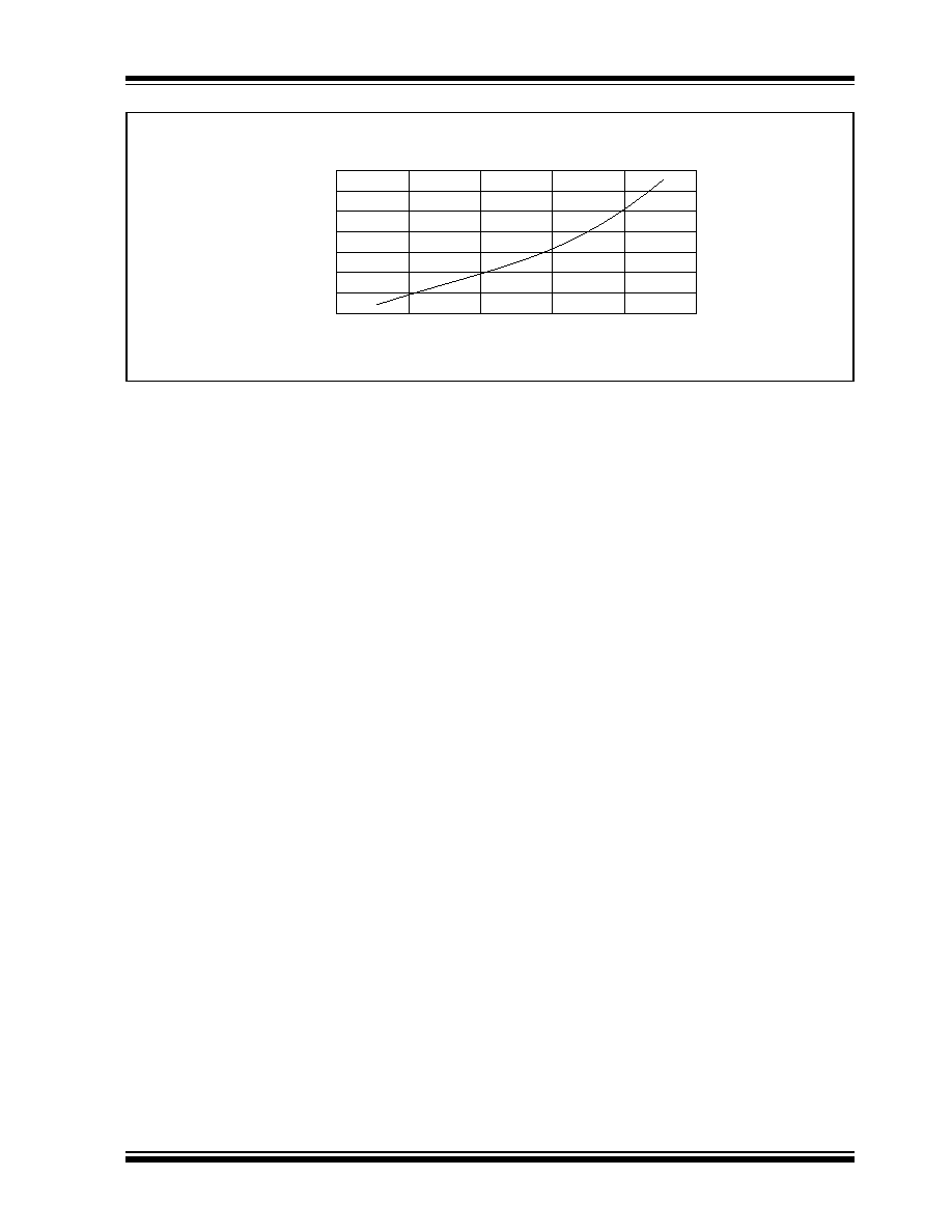
TC7652
-6
-4
-2
0
2
4
COMMON MODE VOLTAGE (V)
Input Offset Voltage vs Common Mode Voltage
4.0
3.5
3.0
2.5
2.0
1.5
1.0
0.5
INPUT OFFSET
VOLTAGE (µV)
TC7652
DS21464B-page 12
©
2002 Microchip Technology Inc.
6.0
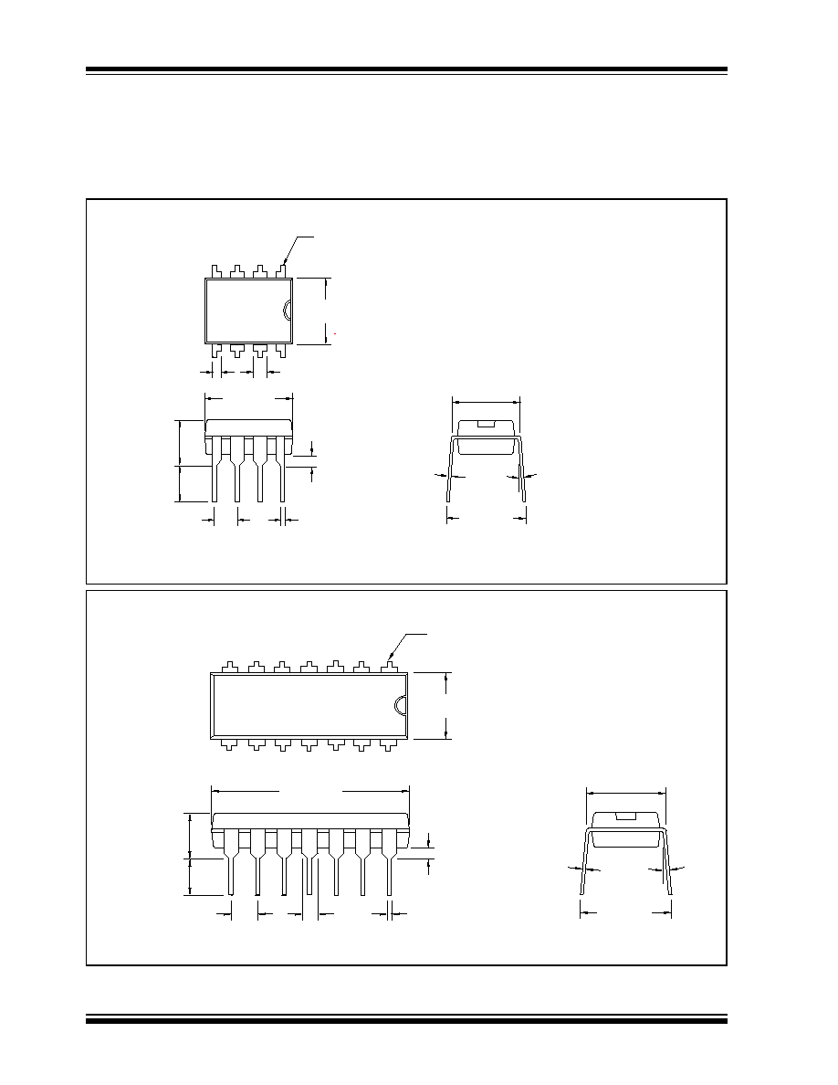
PACKAGING INFORMATION
6.1
Package Marking Information
Package marking information not available at this time.
6.2
Package Dimensions
3
°
MIN.
PIN 1
.260 (6.60)
.240 (6.10)
.045 (1.14)
.030 (0.76)
.070 (1.78)
.040 (1.02)
.400 (10.16)
.348 (8.84)
.200 (5.08)
.140 (3.56)
.150 (3.81)
.115 (2.92)
.110 (2.79)
.090 (2.29)
.022 (0.56)
.015 (0.38)
.040 (1.02)
.020 (0.51)
.015 (0.38)
.008 (0.20)
.310 (7.87)
.290 (7.37)
.400 (10.16)
.310 (7.87)
8-Pin Plastic DIP
Dimensions: inches (mm)
.260 (6.60)
.240 (6.10)
.770 (19.56)
.745 (18.92)
.310 (7.87)
.290 (7.37)
.040 (1.02)
.020 (0.51)
.070 (1.78)
.045 (1.14)
.022 (0.56)
.015 (0.38)
.110 (2.79)
.090 (2.29)
.200 (5.08)
.140 (3.56)
.150 (3.81)
.115 (2.92)
PIN 1
14-Pin PDIP (Narrow)
.015 (0.38)
.008 (0.20)
3
°
MIN.
.400 (10.16)
.310 (7.87)
Dimensions: inches (mm)

2002 Microchip Technology Inc.
DS21464B-page 13
TC7652
SALES AND SUPPORT
Data Sheets
Products supported by a preliminary Data Sheet may have an errata sheet describing minor operational differences and recom-
mended workarounds. To determine if an errata sheet exists for a particular device, please contact one of the following:
1.
Your local Microchip sales office
2.
The Microchip Corporate Literature Center U.S. FAX: (480) 792-7277
3.
The Microchip Worldwide Site (www.microchip.com)
Please specify which device, revision of silicon and Data Sheet (include Literature #) you are using.
New Customer Notification System
Register on our web site (www.microchip.com/cn) to receive the most current information on our products.

TC7652
DS21464B-page 14
2002 Microchip Technology Inc.
NOTES:
2002 Microchip Technology Inc.
DS21464B - page 15
Information contained in this publication regarding device
applications and the like is intended through suggestion only
and may be superseded by updates. It is your responsibility to
ensure that your application meets with your specifications.
No representation or warranty is given and no liability is
assumed by Microchip Technology Incorporated with respect
to the accuracy or use of such information, or infringement of
patents or other intellectual property rights arising from such
use or otherwise. Use of Microchip's products as critical com-
ponents in life support systems is not authorized except with
express written approval by Microchip. No licenses are con-
veyed, implicitly or otherwise, under any intellectual property
rights.
Trademarks
The Microchip name and logo, the Microchip logo, FilterLab,
K
EE
L
OQ
, microID,
MPLAB, PIC, PICmicro, PICMASTER,
PICSTART, PRO MATE, SEEVAL and The Embedded Control
Solutions Company are registered trademarks of Microchip Tech-
nology Incorporated in the U.S.A. and other countries.
dsPIC, ECONOMONITOR, FanSense, FlexROM, fuzzyLAB,
In-Circuit Serial Programming, ICSP, ICEPIC, microPort,
Migratable Memory, MPASM, MPLIB, MPLINK, MPSIM,
MXDEV, PICC, PICDEM, PICDEM.net, rfPIC, Select Mode
and Total Endurance are trademarks of Microchip Technology
Incorporated in the U.S.A.
Serialized Quick Turn Programming (SQTP) is a service mark
of Microchip Technology Incorporated in the U.S.A.
All other trademarks mentioned herein are property of their
respective companies.
© 2002, Microchip Technology Incorporated, Printed in the
U.S.A., All Rights Reserved.
Printed on recycled paper.
Microchip received QS-9000 quality system
certification for its worldwide headquarters,
design and wafer fabrication facilities in
Chandler and Tempe, Arizona in July 1999
and Mountain View, California in March 2002.
The Company's quality system processes and
procedures are QS-9000 compliant for its
PICmicro
®
8-bit MCUs, K
EE
L
OQ
®
code hopping
devices, Serial EEPROMs, microperipherals,
non-volatile memory and analog products. In
addition, Microchip's quality system for the
design and manufacture of development
systems is ISO 9001 certified.
DS21464B-page 16
©
2002 Microchip Technology Inc.
AMERICAS
Corporate Office
2355 West Chandler Blvd.
Chandler, AZ 85224-6199
Tel: 480-792-7200 Fax: 480-792-7277
Technical Support: 480-792-7627
Web Address: http://www.microchip.com
Rocky Mountain
2355 West Chandler Blvd.
Chandler, AZ 85224-6199
Tel: 480-792-7966 Fax: 480-792-7456
Atlanta
500 Sugar Mill Road, Suite 200B
Atlanta, GA 30350
Tel: 770-640-0034 Fax: 770-640-0307
Boston
2 Lan Drive, Suite 120
Westford, MA 01886
Tel: 978-692-3848 Fax: 978-692-3821
Chicago
333 Pierce Road, Suite 180
Itasca, IL 60143
Tel: 630-285-0071 Fax: 630-285-0075
Dallas
4570 Westgrove Drive, Suite 160
Addison, TX 75001
Tel: 972-818-7423 Fax: 972-818-2924
Detroit
Tri-Atria Office Building
32255 Northwestern Highway, Suite 190
Farmington Hills, MI 48334
Tel: 248-538-2250 Fax: 248-538-2260
Kokomo
2767 S. Albright Road
Kokomo, Indiana 46902
Tel: 765-864-8360 Fax: 765-864-8387
Los Angeles
18201 Von Karman, Suite 1090
Irvine, CA 92612
Tel: 949-263-1888 Fax: 949-263-1338
New York
150 Motor Parkway, Suite 202
Hauppauge, NY 11788
Tel: 631-273-5305 Fax: 631-273-5335
San Jose
Microchip Technology Inc.
2107 North First Street, Suite 590
San Jose, CA 95131
Tel: 408-436-7950 Fax: 408-436-7955
Toronto
6285 Northam Drive, Suite 108
Mississauga, Ontario L4V 1X5, Canada
Tel: 905-673-0699 Fax: 905-673-6509
ASIA/PACIFIC
Australia
Microchip Technology Australia Pty Ltd
Suite 22, 41 Rawson Street
Epping 2121, NSW
Australia
Tel: 61-2-9868-6733 Fax: 61-2-9868-6755
China - Beijing
Microchip Technology Consulting (Shanghai)
Co., Ltd., Beijing Liaison Office
Unit 915
Bei Hai Wan Tai Bldg.
No. 6 Chaoyangmen Beidajie
Beijing, 100027, No. China
Tel: 86-10-85282100 Fax: 86-10-85282104
China - Chengdu
Microchip Technology Consulting (Shanghai)
Co., Ltd., Chengdu Liaison Office
Rm. 2401, 24th Floor,
Ming Xing Financial Tower
No. 88 TIDU Street
Chengdu 610016, China
Tel: 86-28-6766200 Fax: 86-28-6766599
China - Fuzhou
Microchip Technology Consulting (Shanghai)
Co., Ltd., Fuzhou Liaison Office
Unit 28F, World Trade Plaza
No. 71 Wusi Road
Fuzhou 350001, China
Tel: 86-591-7503506 Fax: 86-591-7503521
China - Shanghai
Microchip Technology Consulting (Shanghai)
Co., Ltd.
Room 701, Bldg. B
Far East International Plaza
No. 317 Xian Xia Road
Shanghai, 200051
Tel: 86-21-6275-5700 Fax: 86-21-6275-5060
China - Shenzhen
Microchip Technology Consulting (Shanghai)
Co., Ltd., Shenzhen Liaison Office
Rm. 1315, 13/F, Shenzhen Kerry Centre,
Renminnan Lu
Shenzhen 518001, China
Tel: 86-755-2350361 Fax: 86-755-2366086
Hong Kong
Microchip Technology Hongkong Ltd.
Unit 901-6, Tower 2, Metroplaza
223 Hing Fong Road
Kwai Fong, N.T., Hong Kong
Tel: 852-2401-1200 Fax: 852-2401-3431
India
Microchip Technology Inc.
India Liaison Office
Divyasree Chambers
1 Floor, Wing A (A3/A4)
No. 11, O'Shaugnessey Road
Bangalore, 560 025, India
Tel: 91-80-2290061 Fax: 91-80-2290062
Japan
Microchip Technology Japan K.K.
Benex S-1 6F
3-18-20, Shinyokohama
Kohoku-Ku, Yokohama-shi
Kanagawa, 222-0033, Japan
Tel: 81-45-471- 6166 Fax: 81-45-471-6122
Korea
Microchip Technology Korea
168-1, Youngbo Bldg. 3 Floor
Samsung-Dong, Kangnam-Ku
Seoul, Korea 135-882
Tel: 82-2-554-7200 Fax: 82-2-558-5934
Singapore
Microchip Technology Singapore Pte Ltd.
200 Middle Road
#07-02 Prime Centre
Singapore, 188980
Tel: 65-6334-8870 Fax: 65-6334-8850
Taiwan
Microchip Technology Taiwan
11F-3, No. 207
Tung Hua North Road
Taipei, 105, Taiwan
Tel: 886-2-2717-7175 Fax: 886-2-2545-0139
EUROPE
Denmark
Microchip Technology Nordic ApS
Regus Business Centre
Lautrup hoj 1-3
Ballerup DK-2750 Denmark
Tel: 45 4420 9895 Fax: 45 4420 9910
France
Microchip Technology SARL
Parc d'Activite du Moulin de Massy
43 Rue du Saule Trapu
Batiment A - ler Etage
91300 Massy, France
Tel: 33-1-69-53-63-20 Fax: 33-1-69-30-90-79
Germany
Microchip Technology GmbH
Gustav-Heinemann Ring 125
D-81739 Munich, Germany
Tel: 49-89-627-144 0 Fax: 49-89-627-144-44
Italy
Microchip Technology SRL
Centro Direzionale Colleoni
Palazzo Taurus 1 V. Le Colleoni 1
20041 Agrate Brianza
Milan, Italy
Tel: 39-039-65791-1 Fax: 39-039-6899883
United Kingdom
Arizona Microchip Technology Ltd.
505 Eskdale Road
Winnersh Triangle
Wokingham
Berkshire, England RG41 5TU
Tel: 44 118 921 5869 Fax: 44-118 921-5820
03/01/02
W
ORLDWIDE
S
ALES
AND
S
ERVICE