 | ÐлекÑÑоннÑй компоненÑ: TC7660IJA | СкаÑаÑÑ:  PDF PDF  ZIP ZIP |
Äîêóìåíòàöèÿ è îïèñàíèÿ www.docs.chipfind.ru
TC7660
TC7660-7 9/30/96
EVALUATION
KIT
AVAILABLE
© 2001 Microchip Technology Inc. DS21465A
CHARGE PUMP DC-TO-DC VOLTAGE CONVERTER
FEATURES
s
Converts +5V Logic Supply to
±
5V System
s
Wide Input Voltage Range .................... 1.5V to 10V
s
Efficient Voltage Conversion ......................... 99.9%
s
Excellent Power Efficiency ............................... 98%
s
Low Power Supply ............................... 80
µ
A @ 5V
IN
s
Low Cost and Easy to Use
-- Only Two External Capacitors Required
s
RS232 Negative Power Supply
s
Available in Small Outline (SO) Package
s
Improved ESD Protection ....................... Up to 3kV
s
No Dx Diode Required for High Voltage Operation
GENERAL DESCRIPTION
The TC7660 is a pin-compatible replacement for the
Industry standard TC7660 charge pump voltage converter.
It converts a +1.5V to +10V input to a corresponding 1.5V
to -10V output using only two low-cost capacitors, eliminat-
ing inductors and their associated cost, size and EMI.
The on-board oscillator operates at a nominal fre-
quency of 10kHz. Operation below 10kHz (for lower supply
current applications) is possible by connecting an external
capacitor from OSC to ground (with pin 1 open).
The TC7660 is available in both 8-pin DIP and 8-pin
SOIC packages in commercial and extended temperature
ranges.
ORDERING INFORMATION
Temperature
Part No.
Package
Range
TC7660COA
8-Pin SOIC
0
°
C to +70
°
C
TC7660CPA
8-Pin Plastic DIP
0
°
C to +70
°
C
TC7660EOA
8-Pin SOIC
40
°
C to +85
°
C
TC7660EPA
8-Pin Plastic DIP
40
°
C to +85
°
C
TC7660IJA
8-Pin CerDIP
40
°
C to +85
°
C
TC7660MJA
8-Pin CerDIP
55
°
C to +125
°
C
TC7660EV
Evaluation Kit for
Charge Pump Family
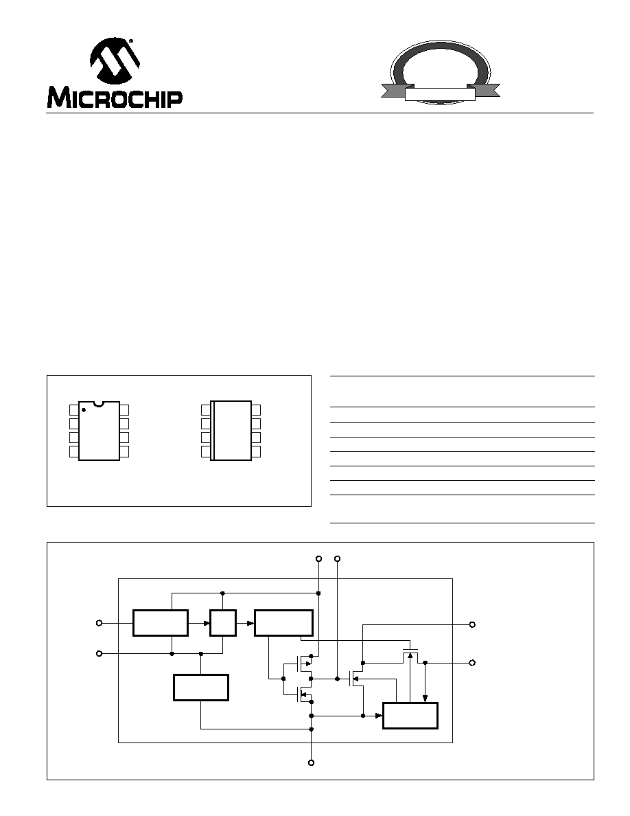
FUNCTIONAL BLOCK DIAGRAM
1
2
3
4
8
7
6
5
TC7660CPA
TC7660EPA
TC7660IJA
NC
CAP +
GND
CAP
NC
CAP +
GND
CAP
VOUT
LOW
VOLTAGE (LV)
OSC
+
V
VOUT
LOW
VOLTAGE (LV)
OSC
+
V
NC = NO INTERNAL CONNECTION
1
2
3
4
8
7
6
5
TC7660COA
TC7660CPA
TC7660
GND
INTERNAL
VOLTAGE
REGULATOR
RC
OSCILLATOR
VOLTAGE
LEVEL
TRANSLATOR
÷
2
V + CAP +
8
2
7
6
OSC
LV
3
LOGIC
NETWORK
VOUT
5
CAP
4
PIN CONFIGURATION (DIP and SOIC)
2
TC7660
CHARGE PUMP DC-TO-DC
VOLTAGE CONVERTER
© 2001 Microchip Technology Inc. DS21465A
TC7660-7 9/30/96
ABSOLUTE MAXIMUM RATINGS*
Supply Voltage ...................................................... +10.5V
LV and OSC Inputs
Voltage (Note 1) .......................... 0.3V to (V
+
+0.3V)
for V
+
< 5.5V
(V
+
5.5V) to (V
+
+0.3V)
for V
+
> 5.5V
Current Into LV (Note 1) ..................... 20
µ
A for V
+
> 3.5V
Output Short Duration (V
SUPPLY
5.5V) ........ Continuous
Power Dissipation (T
A
70
°
C) (Note 2)
CerDIP ............................................................ 800mW
Plastic DIP ...................................................... 730mW
SOIC ............................................................... 470mW
Operating Temperature Range
C Suffix .................................................. 0
°
C to +70
°
C
I Suffix ............................................... 25
°
C to +85
°
C
E Suffix ............................................. 40
°
C to +85
°
C
M Suffix ........................................... 55
°
C to +125
°
C
Storage Temperature Range ................ 65
°
C to +150
°
C
Lead Temperature (Soldering, 10 sec) ................. +300
°
C
*Static-sensitive device. Unused devices must be stored in conductive
material. Protect devices from static discharge and static fields. Stresses
above those listed under "Absolute Maximum Ratings" may cause perma-
nent damage to the device. These are stress ratings only and functional
operation of the device at these or any other conditions above those
indicated in the operation sections of the specifications is not implied.
Exposure to absolute maximum rating conditions for extended periods
may affect device reliability.
ELECTRICAL CHARACTERISTICS:
Specifications Measured Over Operating Temperature Range With,
V
+
= 5V, C
OSC
= 0, Test Circuit (Figure 1), unless otherwise indicated.
Symbol
Parameter
Test Conditions
Min
Typ
Max
Unit
I
+
Supply Current
R
L
=
--
80
180
µ
A
V
+
H
Supply Voltage Range, High
Min
T
A
Max,
3
--
10
V
R
L
= 10 k
, LV Open
V
+
L
Supply Voltage Range, Low
Min
T
A
Max,
1.5
--
3.5
V
R
L
= 10 k
, LV to GND
R
OUT
Output Source Resistance
I
OUT
= 20mA, T
A
= 25
°
C
--
70
100
I
OUT
= 20mA, 0
°
C
T
A
+70
°
C
--
--
120
(C Device)
I
OUT
= 20mA, 40
°
C
T
A
+85
°
C
--
--
130
(I Device)
I
OUT
= 20mA, 55
°
C
T
A
+125
°
C
--
104
150
(M Device)
V
+
= 2V, I
OUT
= 3 mA, LV to GND
--
150
300
0
°
C
T
A
+70
°
C
V
+
= 2V, I
OUT
= 3 mA, LV to GND
--
160
600
55
°
C
T
A
+125
°
C (Note 3)
F
OSC
Oscillator Frequency
Pin 7 open
--
10
--
kHz
P
EFF
Power Efficiency
R
L
= 5k
95
98
--
%
V
OUT
E
FF
Voltage Conversion Efficiency
R
L
=
97
99.9
--
%
Z
OSC
Oscillator Impedance
V
+
= 2V
--
1
--
M
V
+
= 5V
--
100
--
k
NOTES: 1. Connecting any input terminal to voltages greater than V
+
or less than GND may cause destructive latch-up. It is recommended that no
inputs from sources operating from external supplies be applied prior to "power up" of the TC7660.
2. Derate linearly above 50
°
C by 5.5 mW/
°
C.
3. TC7660M only.
4. The TC7660 can be operated without the Dx diode over full temperature and voltage range.
3
TC7660
CHARGE PUMP DC-TO-DC
VOLTAGE CONVERTER
© 2001 Microchip Technology Inc. DS21465A
TC7660-7 9/30/96
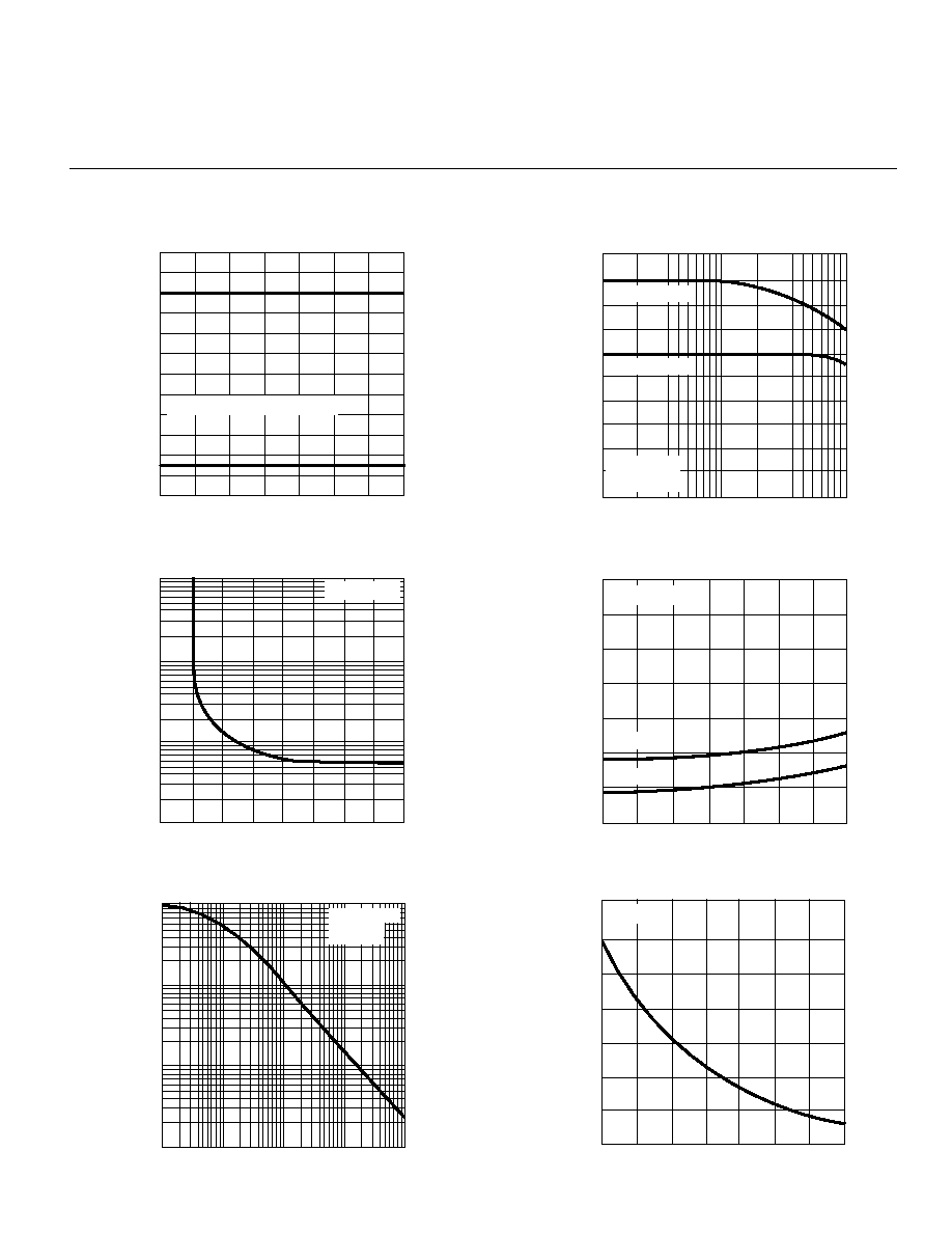
TYPICAL PERFORMANCE CHARACTERISTICS
(Circuit of Figure 1)
500
450
400
200
150
100
50
0
55
25
0
+25
+50
+75 +100 +125
TEMPERATURE (
°
C)
Output Source Resistance vs. Temperature
OUTPUT SOURCE RESISTANCE (
)
V + = +2V
V + = +5V
25
0
+25
+75 +100 +125
12
10
8
6
4
2
+50
Operating Voltage vs. Temperature
55
SUPPLY VOLTAGE (V)
TEMPERATURE (
°
C)
0
7
8
10k
1k
100
OUTPUT SOURCE RESISTANCE (
)
TA = +25
°
C
Output Source Resistance vs. Supply Voltage
6
5
4
3
2
1
0
SUPPLY VOLTAGE (V)
OSCILLATOR FREQUENCY (Hz)
100
POWER CONVERSION EFFICIENCY (%)
98
96
92
90
88
86
84
82
80
94
100
1k
10k
Power Conversion Eff. vs. Osc. Freq.
TEMPERATURE (
°
C)
OSCILLATOR FREQUENCY (kHz)
Unloaded Osc. Freq. vs. Temperature
20
55
18
16
14
12
10
8
6
25
0
+25 +50
+75 +100 +125
V+ = +5V
OSCILLATOR CAPACITANCE (pF)
10k
OSCILLATOR FREQUENCY (Hz)
1
Freq. of Osc. vs. Ext. Osc. Capacitance
1k
100
10
10
100
1000
10k
IOUT = 1 mA
TA = +25
°
C
V+ = +5V
TA = +25
°
C
V+ = +5V
IOUT = 1 mA
IOUT = 15 mA
10
SUPPLY VOLTAGE RANGE
4
TC7660
CHARGE PUMP DC-TO-DC
VOLTAGE CONVERTER
© 2001 Microchip Technology Inc. DS21465A
TC7660-7 9/30/96
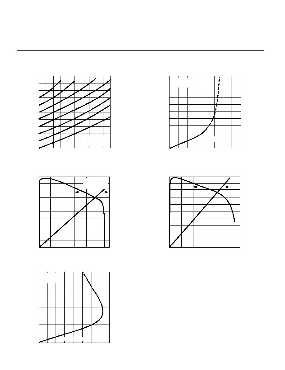
TYPICAL CHARACTERISTICS (Cont.)
2
0
Output Voltage vs. Load Current
OUTPUT VOLTAGE (V)
1
0
1
2
1
2
3
4
5
6
7
8
LOAD CURRENT (mA)
SLOPE 150
TA = +25
°
C
V+ = +2V
LOAD CURRENT (mA)
POWER CONVERSION EFFICIENCY (%)
0
10
20
30
40
50
60
70
80
90
100
0
10
20
30
40
50
60
70
80
90
100
SUPPLY CURRENT (mA) (Note)
10
20
30
40
50
60
TA = +25
°
C
V+ = +5V
Supply Current and Power Conversion Efficiency vs. Load Current
POWER CONVERSION EFFICIENCY (%)
0
LOAD CURRENT (mA)
10
20
30
40
50
60
70
80
90
100
1.5
3.0
4.5
6.0
7.5
9.0
0
2
4
6
8
10
12
14
16
18
20
SUPPLY CURRENT (mA) (Note)
TA = +25
°
C
V+ = 2V
OUTPUT CURRENT (mA)
OUTPUT VOLTAGE (V)
0
0
Output Voltage vs. Output Current
1
2
3
4
5
6
7
8
9
10
10
20 30 40 50
60 70 80
90 100
TA = +25
°
C
LV OPEN
LOAD CURRENT (mA)
OUTPUT VOLTAGE (V)
Output Voltage vs. Load Current
1
0
5
4
3
2
0
1
2
3
4
5
10
20
30
40
50
60
70
80
TA = +25
°
C
V+ = +5V
SLOPE 55
5
TC7660
CHARGE PUMP DC-TO-DC
VOLTAGE CONVERTER
© 2001 Microchip Technology Inc. DS21465A
TC7660-7 9/30/96
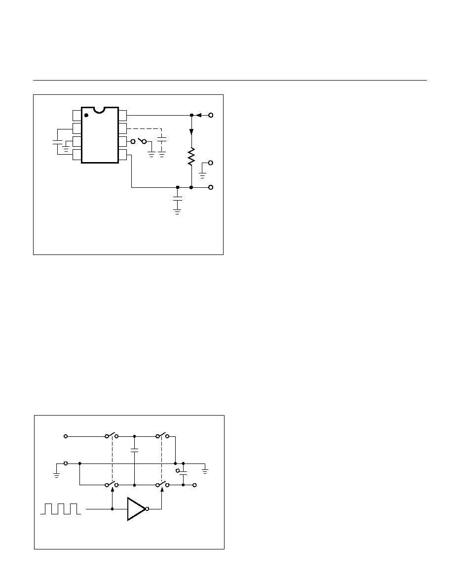
Figure 1. TC7660 Test Circuit
Detailed Description
The TC7660 contains all the necessary circuitry to
implement a voltage inverter, with the exception of two
external capacitors, which may be inexpensive 10
µ
F polar-
ized electrolytic capacitors. Operation is best understood by
considering Figure 2, which shows an idealized voltage
inverter. Capacitor C
1
is charged to a voltage, V
+
, for the half
cycle when switches S
1
and S
3
are closed. (Note: Switches
S
2
and S
4
are open during this half cycle.) During the second
half cycle of operation, switches S
2
and S
4
are closed, with
S
1
and S
3
open, thereby shifting capacitor C
1
negatively by
V
+
volts. Charge is then transferred from C
1
to C
2
, such that
the voltage on C
2
is exactly V
+
, assuming ideal switches and
no load on C
2
.
V+
GND
S3
S1
S2
S4
C2
VOUT
= VIN
Figure 2. Idealized Charge Pump Inverter
The four switches in Figure 2 are MOS power switches;
S
1
is a P-channel device, and S
2
, S
3
and S
4
are N-channel
devices. The main difficulty with this approach is that in
integrating the switches, the substrates of S
3
and S
4
must
always remain reverse-biased with respect to their sources,
but not so much as to degrade their ON resistances. In
addition, at circuit start-up, and under output short circuit
conditions (V
OUT
= V
+
), the output voltage must be sensed
and the substrate bias adjusted accordingly. Failure to
accomplish this will result in high power losses and probable
device latch-up.
This problem is eliminated in the TC7660 by a logic
network which senses the output voltage (V
OUT
) together
with the level translators, and switches the substrates of S
3
and S
4
to the correct level to maintain necessary reverse
bias.
The voltage regulator portion of the TC7660 is an
integral part of the anti-latch-up circuitry. Its inherent voltage
drop can, however, degrade operation at low voltages. To
improve low-voltage operation, the LV pin should be
connected to GND, disabling the regulator. For supply
voltages greater than 3.5V, the LV terminal must be left
open to ensure latch-up-proof operation and prevent device
damage.
Theoretical Power Efficiency
Considerations
In theory, a capacitive charge pump can approach
100% efficiency if certain conditions are met:
(1) The drive circuitry consumes minimal power.
(2) The output switches have extremely low ON
resistance and virtually no offset.
(3) The impedances of the pump and reservoir
capacitors are negligible at the pump frequency.
1
2
3
4
8
7
6
5
TC7660
+
V+
(+5V)
VO
C1
10
µ
F
COSC
*
+
C2
10
µ
F
IL
RL
NOTES:
For large values of COSC (>1000pF), the values
of C1 and C2 should be increased to 100µF.
IS
*