Äîêóìåíòàöèÿ è îïèñàíèÿ www.docs.chipfind.ru
2002 Microchip Technology Inc.
DS20092A-page 1
M
TC77
Features
· Digital Temperature Sensing in 5-Pin SOT-23A
and 8-Pin SOIC Packages
· Outputs Temperature as a 13-Bit Digital Word
· SPI and MICROWIRETM Compatible Interface
· Solid State Temperature Sensing
· ±1°C (max.) accuracy from +25°C to +65°C
· ±2°C (max.) accuracy from -40°C to +85°C
· ±3°C (max.) accuracy from -55°C to +125°C
· 2.7V to 5.5V Operating Range
· Low Power
- 250 µA (typ.) Continuous Conversion Mode
- 0.1 µA (typ.) Shutdown Mode
Typical Applications
· Thermal Protection for Hard Disk Drives and
Other PC Peripherals
· PC Card Devices for Notebook Computers
· Low Cost Thermostat Controls
· Industrial Control
· Office Equipment
· Cellular Phones
· Thermistor Replacement
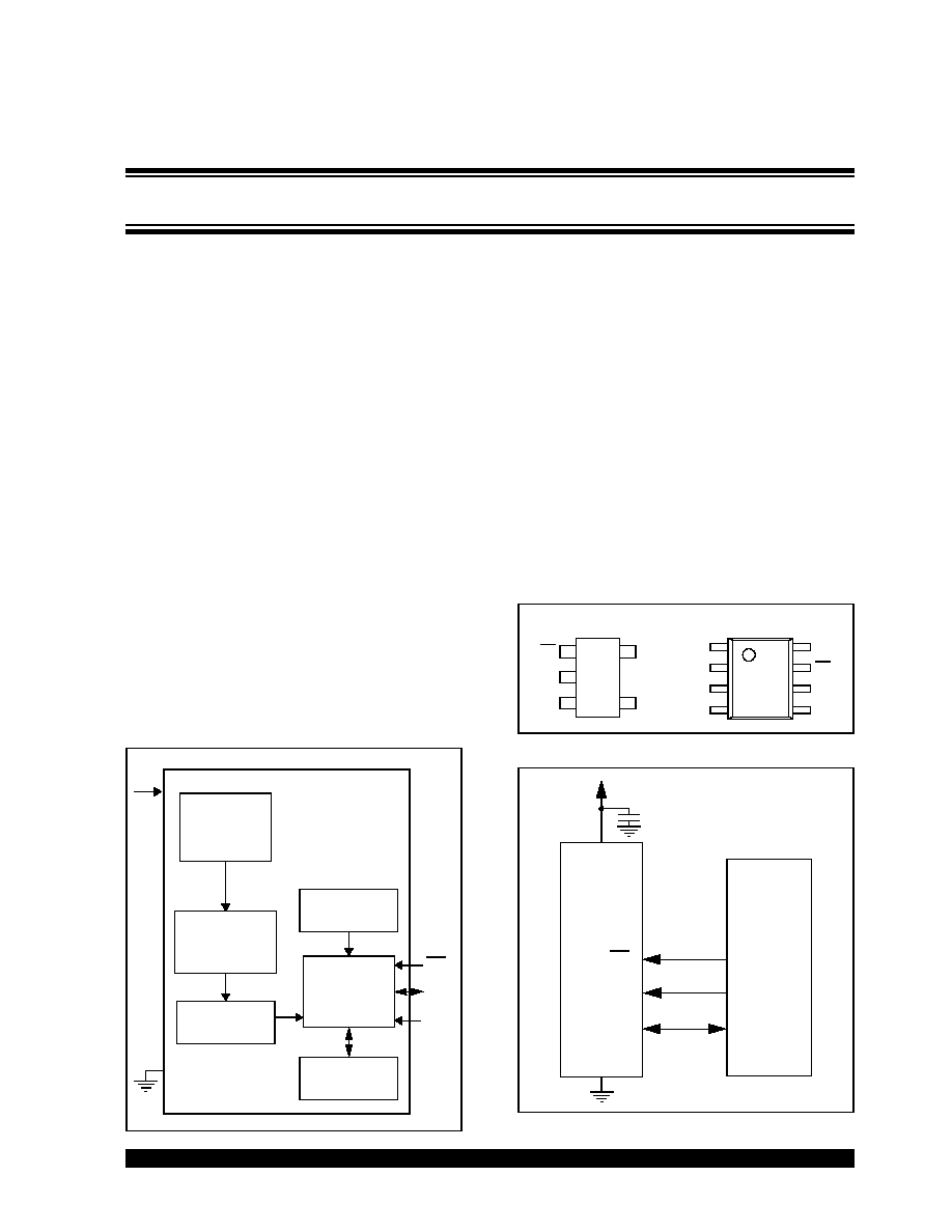
Block Diagram
Description
The TC77 is a serially accessible digital temperature
sensor particularly suited for low cost and small form-
factor applications. Temperature data is converted from
the internal thermal sensing element and made avail-
able at anytime as a 13-bit two's compliment digital
word. Communication with the TC77 is accomplished
via a SPI and MICROWIRE compatible interface. It has
a 12-bit plus sign temperature resolution of 0.0625°C
per Least Significant Bit (LSb). The TC77 offers a tem-
perature accuracy of ±1.0°C (max.) over the tempera-
ture range of +25°C to +65°C. When operating, the
TC77 consumes only 250 µA (typ.). The TC77's Con-
figuration register can be used to activate the low
power Shutdown mode, which has a current consump-
tion of only 0.1 µA (typ.). Small size, low cost and ease
of use make the TC77 an ideal choice for implementing
thermal management in a variety of systems.
Package Types
Typical Application
TC77
Diode
Temperature
Sensor
V
DD
SCK
CS
Serial
Port
Interface
SI/O
13-Bit
Sigma Delta
A/D Converter
Register
Temperature
Register
Internal
Configuration
Manufacturer
ID Register
V
SS
SOT-23-5
1
SOIC
1
V
DD
V
SS
SCK
SI/O
CS
TC77
TC77
SCK
SI/O
V
SS
NC
CS
V
DD
NC
NC
AN0
SCK
SDI
CS
SCK
SI/O
TC77
0.1µF
V
DD
V
SS
V
DD
PICmicro
®
MCU
Thermal Sensor with SPI
TM
Interfa
ce
TC77
DS20092A-page 2
2002 Microchip Technology Inc.
1.0
ELECTRICAL
CHARACTERISTICS
1.1
Absolute Maximum Ratings
V
DD
........................................................................6.0V
All inputs and outputs w.r.t. V
SS
..... -0.3V to V
DD
+0.3V
Storage temperature ..........................-65°C to +150°C
Ambient temp. with power applied .....-55°C to +125°C
Junction Temperature......................................... 150°C
ESD protection on all pins:
Human Body Model (HBM)..............................>4 kV
Machine Model (MM) ......................................>200V
Notice: Stresses above those listed under "Maximum
Ratings" may cause permanent damage to the device. This is
a stress rating only and functional operation of the device at
those or any other conditions above those indicated in the
operation listings of this specification is not implied. Exposure
to maximum rating conditions for extended periods may affect
device reliability.
PIN FUNCTION TABLE
Name
Function
SI/O
Serial Data Pin
SCK
Serial Clock
V
SS
Ground
CS
Chip Select (Active-Low)
NC
No Connection
V
DD
Power Supply
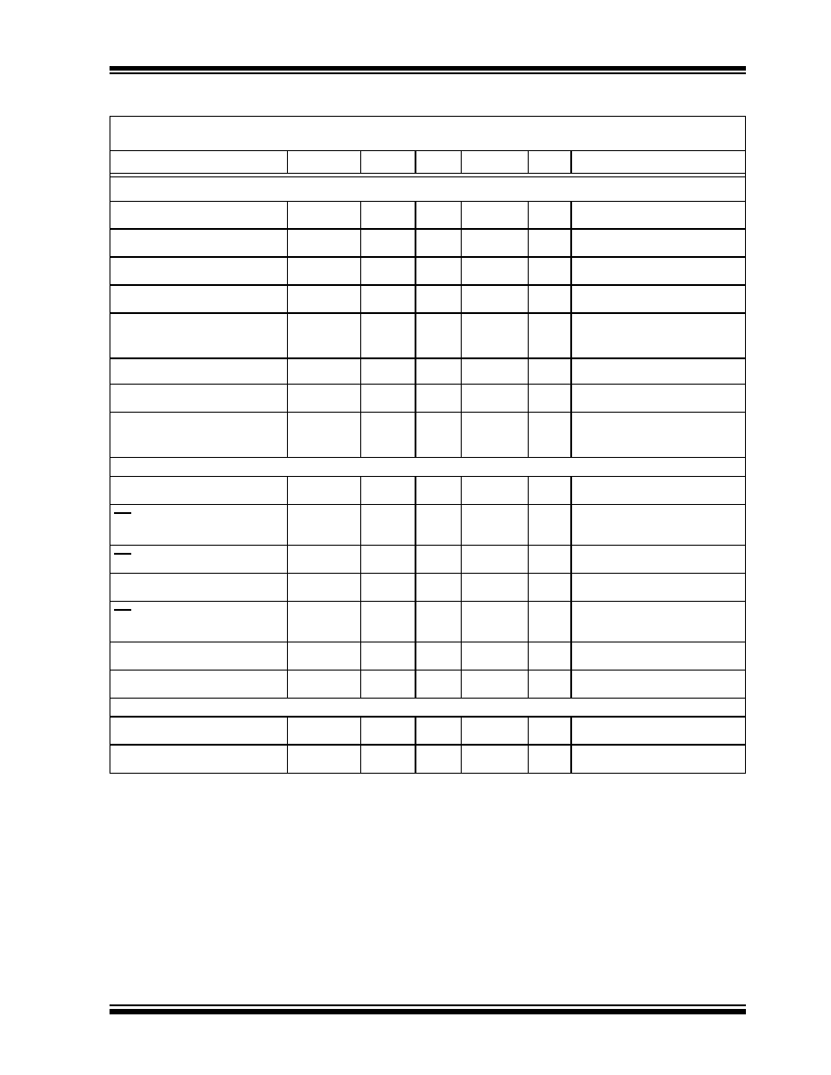
DC CHARACTERISTICS
Electrical Specifications: Unless otherwise noted, all parameters apply at V
DD
= 2.7V to 5.5V and
T
A
= -55°C to +125°C.
Parameters
Sym
Min
Typ
Max
Units
Conditions
Power Supply
Operating Voltage Range
V
DD
2.7
--
5.5
V
Note 1
Operating Current
I
DD
--
250
400
µA
Continuous Temperature
Conversion Mode
Power-On Reset Threshold
V
POR
1.2
1.6
2.2
V
V
DD
falling or rising edge
Standby Supply Current
I
DD-
STANDBY
--
0.1
1.0
µA
Shutdown Mode
Temperature to Bits Converter
Resolution
--
13
--
Bits
ADC LSb = 0.0625°C/bit
(Note 4)
Temperature Conversion Time
t
CT
--
300
400
ms
Temperature Accuracy
(Note 1)
T
ERR
-1.0
-2.0
-3.0
--
--
--
+1.0
+2.0
+3.0
°C
+25°C < T
A
< +65°C
-40°C < T
A
< +85°C
-55°C < T
A
< +125°C
TC77-3.3MXX: V
DD
= 3.3V
TC77-5.0MXX: V
DD
= 5.0V
Note 1: The TC77-3.3MXX and TC77-5.0MXX will operate from a supply voltage of 2.7V to 5.5V. However, the tem-
perature accuracy of the TC77-3.3MXX and TC77-5.0MXX is specified at the nominal operating voltages of
3.3V and 5.0V, respectively. As V
DD
varies from the nominal operating value, the accuracy may be
degraded (Refer to Figures 2-6 and 2-7).
2: All time measurements are measured with respect to the 50% point of the signal.
3: Load Capacitance, C
L
= 80 pF, is used for AC timing measurements of output signals.
4: Resolution = Temperature Range/No. of Bits = (+255°C -256°C) / (2
13
)
Resolution = 512/8192 = 0.0625°C/Bit
2002 Microchip Technology Inc.
DS20092A-page 3
TC77
Digital Input/Output
High Level Input Voltage
V
IH
0.7 V
DD
--
V
DD
+ 0.3
V
Low Level Input Voltage
V
IL
-0.3
--
0.3 V
DD
V
High Level Output Voltage
V
OH
2.4
--
--
V
I
OH
= -400 µA
Low Level Output Voltage
V
OL
--
--
0.4
V
I
OL
= +2 mA
Input Current
I
IN(0),
I
IN(1)
-1.0
-1.0
--
--
+1.0
+1.0
µA
V
IN
= GND
V
IN
= V
DD
Input Hysteresis
0.35
0.8
--
V
SI/O, SCK
Pin Capacitance
C
IN
, C
OUT
--
20
--
pF
Tri-state Output Leakage
Current
I
O_LEAK
-1.0
--
--
--
--
+1.0
µA
V
O
= GND
V
O
= V
DD
Serial Port AC Timing (Notes 2, 3)
Clock Frequency
f
CLK
DC
--
7.0
MHz
CS Fall to First Rising SCK
Edge
t
CS-SCK
100
--
--
ns
CS Low to Data Out Delay
t
CS-SI/O
--
--
70
ns
SCK Fall to Data Out Delay
t
DO
--
--
100
ns
CS High to Data Out
Tri-state
t
DIS
--
--
200
ns
SCK High to Data In Hold Time
t
HD
50
--
--
ns
Data In Set-up Time
t
SU
30
--
--
ns
Thermal Package Resistance
Thermal Resistance, SOT23-5
JA
--
230
--
°C/W
Thermal Resistance, 8L-SOIC
JA
--
163
--
°C/W
DC CHARACTERISTICS (CONTINUED)
Electrical Specifications: Unless otherwise noted, all parameters apply at V
DD
= 2.7V to 5.5V and
T
A
= -55°C to +125°C.
Parameters
Sym
Min
Typ
Max
Units
Conditions
Note 1: The TC77-3.3MXX and TC77-5.0MXX will operate from a supply voltage of 2.7V to 5.5V. However, the tem-
perature accuracy of the TC77-3.3MXX and TC77-5.0MXX is specified at the nominal operating voltages of
3.3V and 5.0V, respectively. As V
DD
varies from the nominal operating value, the accuracy may be
degraded (Refer to Figures 2-6 and 2-7).
2: All time measurements are measured with respect to the 50% point of the signal.
3: Load Capacitance, C
L
= 80 pF, is used for AC timing measurements of output signals.
4: Resolution = Temperature Range/No. of Bits = (+255°C -256°C) / (2
13
)
Resolution = 512/8192 = 0.0625°C/Bit

TC77
DS20092A-page 4
2002 Microchip Technology Inc.
FIGURE 1-1:
Timing Diagrams.
CS
SCK
1/f
CLK
SI/O
t
DO
LSb
t
DIS
HI-Z
Data Output Timing
MSb
t
CS-SI/O
t
HD
t
SU
SI/O
SCK
CS
HI-Z
SI/O
SCK
CS
HI-Z
t
HD
t
SU
HI-Z
t
CS-SCK
SI/O Data Input Set-up and Hold Timing (Data is clocked on the rising edge of SCK)
2002 Microchip Technology Inc.
DS20092A-page 5
TC77
2.0
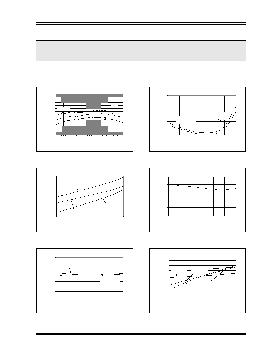
TYPICAL PERFORMANCE CURVES
Note: Unless otherwise indicated, all parameters apply at V
DD
= 3.3V for the TC77-3.3MXX and V
DD
= 5.0V for the TC77-
5.0MXX, and T
A
= -55°C to +125°C. The TC77-3.3MXX and TC77-5.0MXX will operate from a supply voltage of 2.7V
to 5.5V. However, the temperature accuracy of the TC77-3.3MXX and TC77-5.0MXX is specified at the nominal oper-
ating voltages of 3.3V and 5.0V, respectively.
FIGURE 2-1:
Accuracy vs. Temperature
(TC77-XXMXX)
.
FIGURE 2-2:
Supply Current vs. Supply
Voltage (TC77-XXMXX).
FIGURE 2-3:
Supply Current vs.
Temperature.
FIGURE 2-4:
Shutdown Current vs.
Temperature.
FIGURE 2-5:
Power-On Reset Voltage vs.
Temperature (TC77-XXMXX).
FIGURE 2-6:
Temperature Accuracy vs.
Supply Voltage (TC77-3.3MXX).
Note:
The graphs and tables provided following this note are a statistical summary based on a limited number of
samples and are provided for informational purposes only. The performance characteristics listed herein
are not tested or guaranteed. In some graphs or tables, the data presented may be outside the specified
operating range (e.g., outside specified power supply range) and therefore outside the warranted range.
-3.5
-3
-2.5
-2
-1.5
-1
-0.5
0
0.5
1
1.5
2
2.5
3
3.5
-55 -35 -15
5
25
45
65
85 105 125
Reference Temperature (°C)
Temperature Error (°C)
Upper Specification Limit
Lower Specification Limit
Mean + 3
Mean - 3
Mean
200
210
220
230
240
250
2.7
3.1
3.5
3.9
4.3
4.7
5.1
5.5
Supply Voltage (V)
Supply Current (µA)
T
A
= +25°C
T
A
= +125°C
T
A
= -55°C
0
50
100
150
200
250
300
350
400
-55
-25
5
35
65
95
125
Temperature (°C)
Supply Current (µA)
TC77-5.0MXX
V
DD
= 5.0 V
TC77-3.3MXX
V
DD
= 3.3 V
0.0
0.1
0.2
0.3
-55
-25
5
35
65
95
125
Temperature (°C)
Shutdown Current (µA)
TC77-5.0MXX
V
DD
= 5.0 V
TC77-3.3MXX
V
DD
= 3.3 V
0.0
0.5
1.0
1.5
2.0
2.5
-55
-25
5
35
65
95
125
Temperature (°C)
Power-On Reset Voltage (V)
-0.4
-0.3
-0.2
-0.1
0
0.1
0.2
0.3
0.4
3
3.1
3.2
3.3
3.4
3.5
3.6
Supply Voltage (V)
Temperature Change (°C)
TC77-3.3MXX
T
A
= -25°C
T
A
= +25°C
T
A
= +85°C
Document Outline