 | ÐлекÑÑоннÑй компоненÑ: TC835CBU | СкаÑаÑÑ:  PDF PDF  ZIP ZIP |
Äîêóìåíòàöèÿ è îïèñàíèÿ www.docs.chipfind.ru
©
2002 Microchip Technology Inc.
DS21478B-page 1
TC835
Features
· Upgrade of Pin-Compatible TC7135, ICL7135
· 200kHz Operation
· Single 5V Operation With TC7660
· Multiplexed BCD Data Output
· UART and Microprocessor Interface
· Control Outputs for Auto-Ranging
· Input Sensitivity: 100µV
· No Sample and Hold Required
Applications
· Personal Computer Data Acquisition
· Scales, Panel Meters, Process Controls
· HP-IL Bus Instrumentation
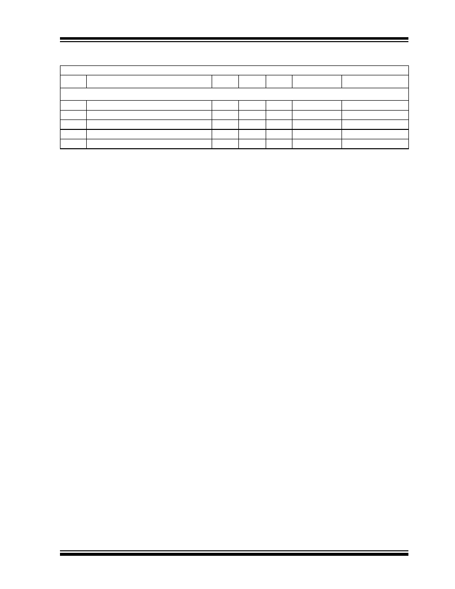
Device Selection Table
General Description
The TC835 is a low power, 4-1/2 digit (0.005%
resolution), BCD analog to digital converter (ADC) that
has been characterized for 200kHz clock rate opera-
tion. The five conversions per second rate is nearly
twice as fast as the ICL7135 or TC7135. The TC835,
like the TC7135, does not use the external diode resis-
tor rollover error compensation circuits required by the
ICL7135.
The multiplexed BCD data output is perfect for interfac-
ing to personal computers. The low cost, greater than
14-bit high-resolution and 100
µ
V sensitivity makes the
TC835 exceptionally cost-effective.
Microprocessor-based data acquisition systems are
supported by the BUSY and STROBE outputs, along
with the RUN/HOLD
input of the
TC835. The
OVERRANGE, UNDERRANGE, BUSY and RUN/
HOLD control functions, plus multiplexed BCD data
outputs, make the TC835 the ideal converter for
µ
P-
based scales, measurement systems and intelligent
panel meters.
The TC835 interfaces with full function LCD and LED
display decoder/drivers. The UNDERRANGE and
OVERRANGE outputs may be used to implement an
auto-ranging scheme or special display functions.
Part Number
Package
Temperature Range
TC835CBU
64-Pin PQFP
0
°
C to +70
°
C
TC835CKW
44-Pin PQFP
0
°
C to +70
°
C
TC835CPI
28-Pin PDIP
0
°
C to +70
°
C
Note:
Tape and Reel available for 44-Pin PQFP
package.
Personal Computer Data Acquisition A/D Converter
TC835
DS21478B-page 2
©
2002 Microchip Technology Inc.
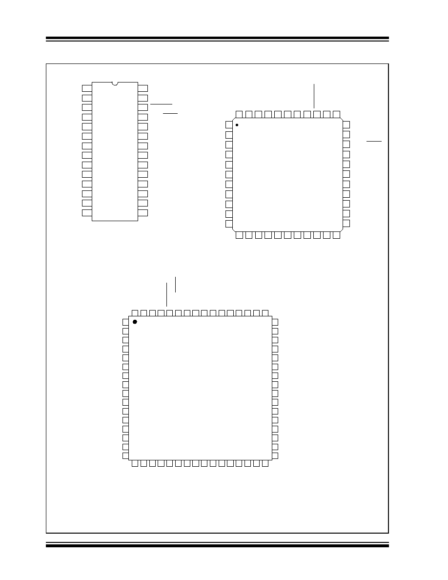
Package Type
NOTES: 1. NC = No internal connection.
2. Pins 9, 25, 40 and 56 are connected to the die substrate. The potential at these pins is approximately V+.
No external connections should be made.
64-Pin PQFP
63
4
3
2
1
16
15
14
10
9
8
7
6
5
12
11
40
41
42
43
44
45
46
34
35
36
37
38
39
48
33
17 18 19 20 21 22 23 24 25 26 27 28 29 30 31
61 60 59 58 57 56 55 54 53 52 51 50 49
64
TC835CBU
INT OUT
NC
AZ IN
V+
NC
+INPUT
NC
BUFF
OUT
BUF CAP
NC
SUB
BUF CAP+
NC
INPUT
NC
NC
NC
NC
NC
NC
D1
DGND
POL
SUB
CLK IN
BUSY
D2
32
NC
62
NC
13
47
NC
NC
NC
NC
NC
NC
NC
NC
NC
OVERRANGE
UNDERRANGE
SUB
V
REF IN
ANALOG COM
NC
NC
D3
NC
NC
NC
NC
D4
B3
B4
B2
SUB
B1
D5
NC
NC
NC
NC
STROBE
RUN/HOLD
TC835CPI
28-Pin PDIP
1
2
3
4
RUN/HOLD
5
6
7
8
9
10
11
12
13
14
28
27
26
25
24
23
22
21
20
19
18
17
16
15
STROBE
OVERRANGE
B4
D3
D2
D1 (LSD)
BUSY
CLOCK IN
POLARITY
DIGTAL GND
UNDERRANGE
B2
(LSB) B1
(MSD) D5
V+
+INPUT
INPUT
C
REF
+
C
REF
-
BUFF OUT
AZ IN
INT OUT
ANALOG
COM
REF IN
V-
D4
B8 (MSD)
27
28
29
30
31
32
33
7
4
3
2
1
TC835CKW
12 13 14 15
17 18
44 43 42 41
39 38
40
16
37 36 35 34
19 20 21 22
26
8
25
9
24
10
23
11
5
6
NC
NC
NC
ANALOG
REF IN
V
UR
OR
NC
NC
NC
NC
DGND
POLARITY
D2
NC
NC
CLK IN
NC
INT OUT
AZ IN
BUFF OUT
REF CAP
INPUT
+INPUT
V+
NC
NC
REF CAP+
NC
NC
(MSD) D5
(LSB) B1
B2
B4
(MSB) B8
D4
D3
NC
NC
D1 (LSD)
BUSY
RUN/HOLD
STROBE
44-Pin PQFP
COMMON
©
2002 Microchip Technology Inc.
DS21478B-page 3
TC835
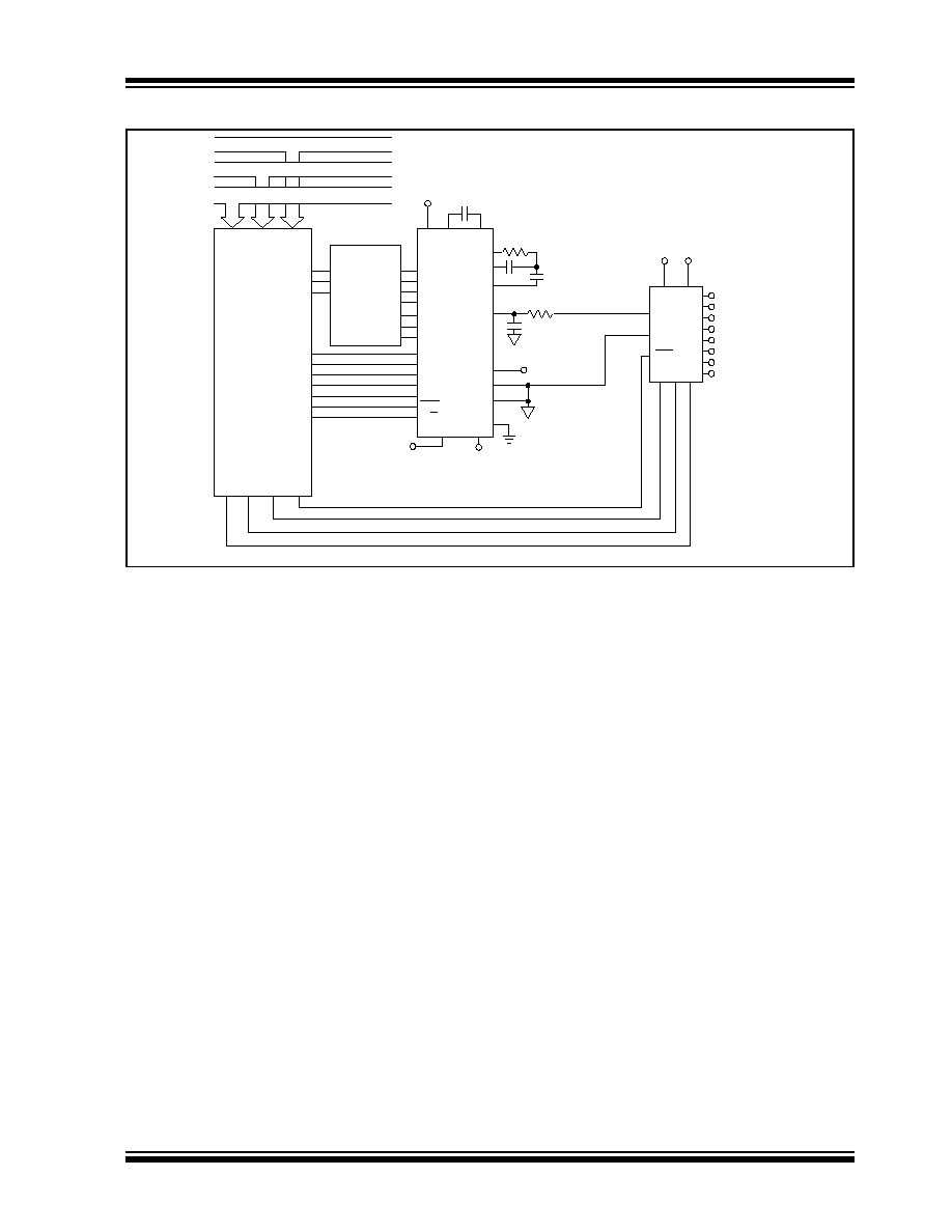
Typical Application
Channel 1
Channel 2
Channel 3
Channel 4
Data Bus
Control
Address Bus
R 6522 P
PA0
PA1
PA2
PA3
PA4
PA5
PA6
PA7
CA1
CA2
PB0
PB3
PB2
PB1
Channel Selection
1Y
2Y
3Y
1B
2B
3B
S
1A
2A
3A
HCTS157
POL
OR
UR
D5
B8
B4
B2
B1
D1
D2
D3
D4
STB
R/H
V+ REF
CAP
BUF
AZ
INT
INPUT+
V
R
Input
Analog
Common
DGND
5V
REF Voltage
+15V -15V
Differential
Multiplexer
DG529
D
A
D
B
WR
A
1
A
0
EN
5V
+
-
F
IN
F
IN
TC835
TC835
DS21478B-page 4
©
2002 Microchip Technology Inc.
1.0
ELECTRICAL
CHARACTERISTICS
Absolute Maximum Ratings*
Positive Supply Voltage ......................................... +6V
Negative Supply Voltage ........................................ -9V
Analog Input Voltage (Pin 9 or 10) ... V+ to V (Note 2)
Reference Input Voltage (Pin 2) ..................... V+ to V
Clock Input Voltage ........................................ 0V to V
+
Operating Temperature Range................0°C to +70°C
Storage Temperature Range ............. -65°C to +150°C
Package Power Dissipation (T
A
70°C)
28-Pin Plastic DIP ............................ 1.14
44-Pin PQFP .................................... 1.00
64-Pin PQFP .................................... 1.14
*Stresses above those listed under "Absolute Maximum Rat-
ings" may cause permanent damage to the device. These are
stress ratings only and functional operation of the device at
these or any other conditions above those indicated in the
operation sections of the specifications is not implied. Expo-
sure to Absolute Maximum Rating conditions for extended
periods may affect device reliability.
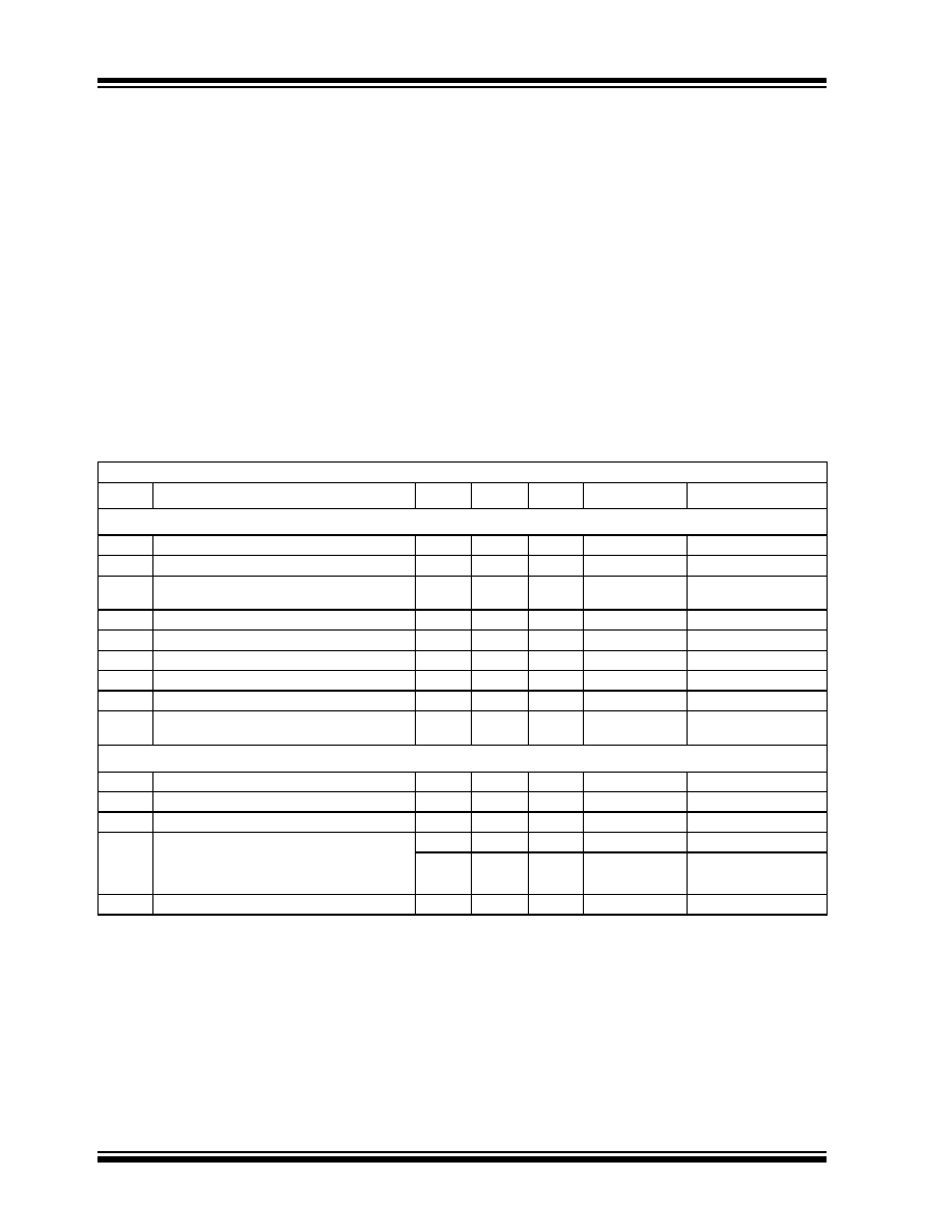
TC835 ELECTRICAL SPECIFICATIONS
Electrical Characteristics: T
A
= +25°C, F
CLOCK
= 200kHz, V+ = +5V, V- = -5V, unless otherwise specified.
Symbol
Parameter
Min
Typ
Max
Unit
Test Conditions
Analog
Display Reading with Zero Volt Input
-0.0000
±0.0000 +0.0000
Display Reading
Note 3, Note 4
TC
Z
Zero Reading Temperature Coefficient
--
0.5
2
µV/°C
V
IN
= 0V, (Note 5)
TC
FS
Full-Scale Temperature Coefficient
--
--
5
ppm/°C
V
IN
= 2V;
(Note 5, Note 6
NL
Nonlinearity Error
--
0.5
1
Count
Note 7
DNL
Differential Linearity Error
--
0.01
--
LSB
Note 7
Display Reading in Ratiometric Operation
+0.9996
+0.9998 +1.0000
Display Reading
V
IN
= V
REF
, (Note 3)
±FSE
± Full Scale Symmetry Error (Rollover Error)
--
0.5
1
Count
V
IN
= +V
IN
, (Note 8)
I
IN
Input Leakage Current
--
1
10
pA
Note 4
e
N
Noise
--
15
--
µ
V
P-P
Peak to Peak Value not
Exceeded 95% of Time
Digital
I
IL
Input Low Current
--
10
100
µ
A
V
IN
= 0V
I
IH
Input High Current
--
0.08
10
µ
A
V
IN
= +5V
V
OL
Output Low Voltage
--
0.2
0.4
V
I
OL
= 1.6mA
V
OH
Output High Voltage;
B
1
, B
2
, B
4
, B
8
, D
1
D
5
Busy, Polarity, Overrange,
Underrange, Strobe
2.4
4.4
5
V
I
OH
= 1mA
4.9
4.99
5
V
I
OH
= 10
µ
A
f
CLK
Clock Frequency
0
200
1200
kHz
Note 10
Note
1:
Functional operation is not implied.
2:
Limit input current to under 100 µA if input voltages exceed supply voltage.
3:
Full scale voltage = 2V.
4:
V
IN
= 0V.
5:
0°C
T
A
+70°C.
6:
External reference temperature coefficient less than 0.01ppm/°C.
7:
-2V
V
IN
+2V. Error of reading from best fit straight line.
8:
|V
IN
| = 1.9959.
9:
Test circuit shown in Figure 1-1.
10: Specification related to clock frequency range over which the TC835 correctly performs its various functions. Increased
errors result at higher operating frequencies.
©
2002 Microchip Technology Inc.
DS21478B-page 5
TC835
Power Supply
V+
Positive Supply Voltage
4
5
6
V
V
Negative Supply Voltage
-3
-5
-8
V
I+
Positive Supply Current
--
1
3
mA
f
CLK
= 0Hz
I
Negative Supply Current
--
0.7
3
mA
f
CLK
= 0Hz
PD
Power Dissipation
--
8.5
30
m
f
CLK
= 0Hz
TC835 ELECTRICAL SPECIFICATIONS (CONTINUED)
Electrical Characteristics: T
A
= +25°C, F
CLOCK
= 200kHz, V+ = +5V, V- = -5V, unless otherwise specified.
Symbol
Parameter
Min
Typ
Max
Unit
Test Conditions
Note
1:
Functional operation is not implied.
2:
Limit input current to under 100 µA if input voltages exceed supply voltage.
3:
Full scale voltage = 2V.
4:
V
IN
= 0V.
5:
0°C
T
A
+70°C.
6:
External reference temperature coefficient less than 0.01ppm/°C.
7:
-2V
V
IN
+2V. Error of reading from best fit straight line.
8:
|V
IN
| = 1.9959.
9:
Test circuit shown in Figure 1-1.
10: Specification related to clock frequency range over which the TC835 correctly performs its various functions. Increased
errors result at higher operating frequencies.