 | ÐлекÑÑоннÑй компоненÑ: TC850CLW | СкаÑаÑÑ:  PDF PDF  ZIP ZIP |
Äîêóìåíòàöèÿ è îïèñàíèÿ www.docs.chipfind.ru
©
2002 Microchip Technology Inc.
DS21479B-page 1
TC850
Features
· 15-bit Resolution Plus Sign Bit
· Up to 40 Conversions per Second
· Integrating ADC Technique
- Monotonic
- High Noise Immunity
- Auto Zeroed Amplifiers Eliminate Offset
Trimming
· Wide Dynamic Range: 96dB
· Low Input Bias Current: 30pA
· Low Input Noise: 30
µ
V
P-P
· Sensitivity: 100
µ
V
· Flexible Operational Control
· Continuous or On Demand Conversions
· Data Valid Output
· Bus Compatible, 3-State Data Outputs
- 8-Bit Data Bus
- Simple
µ
P Interface
- Two Chip Enables
- Read ADC Result Like Memory
· ± 5V Power Supply Operation: 20m
· 40-Pin Dual-in-Line or 44-Pin PLCC Packages
Applications
· Precision Analog Signal Processor
· Precision Sensor Interface
· High Accuracy DC Measurements
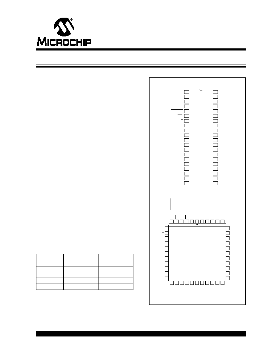
Device Selection Table
Package Types
Part Number
Package
Temperature
Range
TC850CPL
40-Pin PDIP
0
°
C to +70
°
C
TC850IJL
40-Pin CERDIP
-25
°
C to +85
°
C
TC850CLW
44-Pin PLCC
0
°
C to +70
°
C
TC850ILW
44-Pin PLCC
-25
°
C to +85
°
C
TC850CPL
TC850IJL
1
2
3
4
5
6
7
8
9
10
11
12
13
14
15
16
17
18
19
20
40
39
38
37
36
35
34
33
32
31
30
29
28
27
26
25
24
23
22
21
ANALOG
COMMON
C
BUFB
BUFFER
INT
IN
INT
OUT
COMP
40-Pin PDIP/CERDIP
DGND
C
INTA
C
BUFA
C
INTB
IN-
IN+
REF-
TEST
OSC
2
OSC
1
BUSY
DB0
DB1
DB2
DB3
DB4
DB5
DB6
DB7
CS
CE
WR
RD
CONT/DEMAND
OVR/POL
L/H
V
SS
V
DD
REF
1
+
REF
2
+
C
REF1
+
C
REF2
+
C
REF1
-
C
REF2
-
NC = No Internal Connection
44-Pin PLCC
COMP
33
34
35
36
37
38
39
13
10
9
8
7
18 19 20 21
23 24
6
5
4
3
1
44
2
22
43 42 41 40
25 26 27 28
32
14
31
15
30
16
29
17
11
12
TC850CLW
TC850ILW
NC
NC
NC
TEST
DGND
OSC
2
OSC
1
DB0
DB1
DB2
DB3
DB4
NC
DB5
DB6
DB7
CS
BUFFER
BUSY
CE
WR
RD
CONT/DEMAND
REF-
V
DD
REF
1
+
C
REF1
+
C
REF1
-
IN-
IN+
REF
2
+
C
REF2
+
C
REF2
-
ANALOG
COMMON
C
BUFB
C
INTA
C
BUFA
C
INTB
INT
IN
INT
OUT
V
SS
OVR/POL
L/H
15-Bit, Fast Integrating CMOS A/D Converter
TC850
DS21479B-page 2
©
2002 Microchip Technology Inc.
General Description
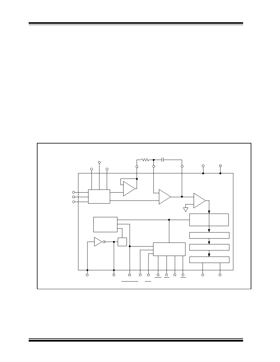
The TC850 is a monolithic CMOS A/D converter (ADC)
with resolution of 15-bits plus sign. It combines a chop-
per-stabilized buffer and integrator with a unique multi-
ple-slope
integration
technique
that
increases
conversion speed. The result is 16 times improvement
in speed over previous 15-bit, monolithic integrating
ADCs (from 2.5 conversions per second up to 40 per
second). Faster conversion speed is especially wel-
come in systems with human interface, such as digital
scales.
The TC850 incorporates an ADC and a
µ
P-compatible
digital interface. Only a voltage reference and a few,
noncritical, passive components are required to form a
complete 15-bit plus sign ADC. CMOS processing pro-
vides the TC850 with high-impedance, differential
inputs. Input bias current is typically only 30pA, permit-
ting direct interface to sensors. Input sensitivity of
100
µ
V per least significant bit (LSB) eliminates the
need for precision external amplifiers. The internal
amplifiers are auto zeroed, ensuring a zero digital out-
put,
with
0V
analog
input.
Zero
adjustment
potentiometers or calibrations are not required.
The TC850 outputs data on an 8-bit, 3-state bus. Digital
inputs are CMOS compatible while outputs are TTL/
CMOS compatible. Chip-enable and byte-select inputs,
combined with an end-of-conversion output, ensures
easy interfacing to a wide variety of microprocessors.
Conversions can be performed continuously or on
command. In continuous mode, data is read as three
consecutive bytes and manipulation of address lines is
not required.
Operating from ±5V supplies, the TC850 dissipates
only 20m
. The TC850 is packaged in a 40-pin plastic
or ceramic dual-in-line package (DIPs) and in a 44-pin
plastic leaded chip carrier (PLCC), surface-mount
package.
Functional Block Diagram
÷4
BUF
INT IN
Buffer
Pinout of 40-Pin Package
Integrator
Comparator
32
23
24
25
36
34
39
15
8
DB7
TC850
REF-
R
INT
C
INT
INT OUT
IN+
-
+
-
+
6-Bit
Up/Down
Counter
-
+
REF
2
+
REF
1
+
DB0
9-Bit
Up/Down
Counter
. . . .
5
3
WR
CONT/
DEMAND
Analog
Mux
31
30
IN-
COMMON
22
40
+5V
5V
18
OSC
2
17
7
L/H
6
OVR/
POL
4
RD
1
CS
2
CE
OSC
1
A/D
Control
Sequencer
Data Latch
Octal 2-Input Mux
3-State Data Bus
Clock
Oscillator
Bus Interface
Decode Logic
©
2002 Microchip Technology Inc.
DS21479B-page 3
TC850
1.0
ELECTRICAL SPECIFICATIONS
Absolute Maximum Ratings*
Positive Supply Voltage..........................................+6V
Negative Supply Voltage ....................................... - 9V
Analog Input Voltage (IN+ pr IN-) .............. V
DD
to V
SS
Voltage Reference Input:
(REF
1
+, REF
1
, REF
2
+).................. V
DD
to V
SS
Logic Input Voltage............. V
DD
+ 0.3V to GND 0.3V
Current Into Any Pin............................................10mA
While Operating ......................................100
µ
A
Ambient Operating Temperature Range
C Device....................................... 0°C to +70°C
I Device......................................-25°C to +85°C
Package Power Dissipation (T
A
70°C)
CerDIP .....................................................2.29
Plastic DIP................................................1.23
Plastic PLCC ...........................................1.23
*Stresses above those listed under "Absolute Maximum Rat-
ings" may cause permanent damage to the device. These are
stress ratings only and functional operation of the device at
these or any other conditions above those indicated in the
operation sections of the specifications is not implied. Expo-
sure to Absolute Maximum Rating conditions for extended
periods may affect device reliability.
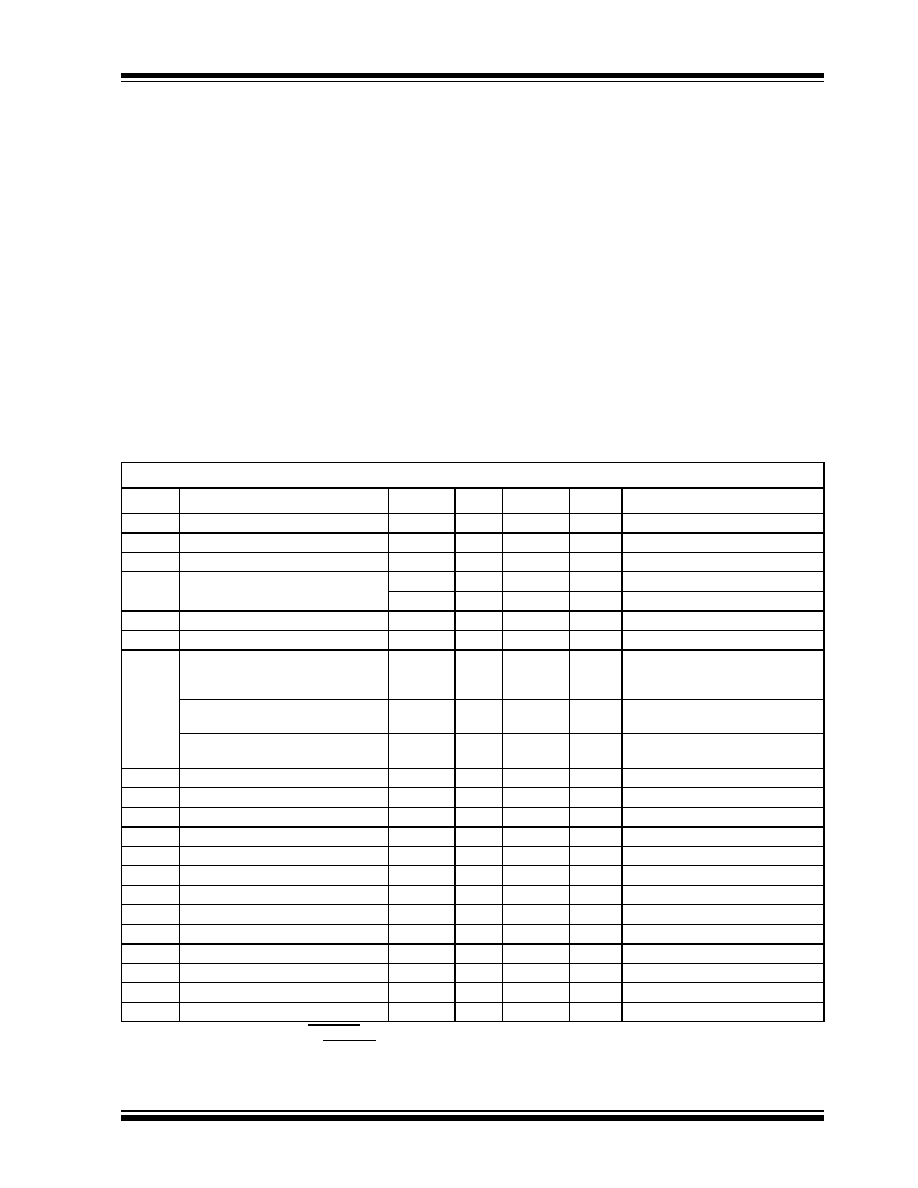
TC850 ELECTRICAL SPECIFICATIONS
Electrical Characteristics: V
S
= ±5V; F
CLK
= 61.44kHz, V
FS
= 3.2768V, T
A
= 25°C, Figure 1-1, unless otherwise specified.
Symbol
Parameter
Min
Typ
Max
Unit
Test Conditions
Zero Scale Error
±0.25
±0.5
LSB
V
IN
= 0V
End Point Linearity Error
--
±1
±2
LSB
-V
FS
V
IN
+V
FS
Differential Nonlinearity
--
±0.1
±0.5
LSB
I
IN
Input Leakage Current
--
30
75
pA
V
IN
= 0V, T
A
= 25°C
--
1.1
3
nA
-25°
T
A
+85°C
V
CMR
Common Mode Voltage Range
V
SS
+ 1.5
--
V
SS
1.5
V
Over Operating Temperature Range
CMRR
Common Mode Rejection Ratio
--
80
--
dB
V
IN
= 0V, V
CM
= ±1V
Full Scale Gain Temperature
Coefficient
--
2
5
ppm/°C External Ref. Temperature
Coefficient = 0 ppm/°C
0°C
T
A
+70°C
Zero Scale Error
Temperature Coefficient
--
0.3
2
µ
V/°C
V
IN
= 0V
0°C
T
A
+70°C
Full Scale Magnitude
Symmetry Error
--
0.5
2
LSB
V
IN
= ±3.275V
e
N
Input Noise
--
30
--
µ
V
P-P
Not Exceeded 95% of Time
I
S
+
Positive Supply Current
--
2
3.5
mA
I
S
Negative Supply Current
--
2
3.5
mA
V
OH
Output High Voltage
3.5
4.9
--
V
I
O
= 500
µ
A
V
OL
Output Low Voltage
--
0.15
0.4
V
I
O
= 1.6mA
I
OP
Output Leakage Current
--
0.1
1
µ
A
Pins 8 -15, High-Impedance State
V
IH
Input High Voltage
3.5
2.3
--
V
Note 3
V
IL
Input Low Voltage
--
2.1
1
V
Note 3
I
PU
Input Pull-Up Current
--
4
--
µ
A
Pins 2, 3, 4, 6, 7; V
IN
= 0V
I
PD
Input Pull-Down Current
--
14
--
µ
A
Pins 1, 5; V
IN
= 5V
I
OSC
Oscillator Output Current
--
140
--
µ
A
Pin 18, V
OUT
= 2.5V
C
IN
Input Capacitance
--
1
--
pF
Pins 1 - 7, 17
C
OUT
Output Capacitance
--
15
--
pF
Pins 8 -15, High-Impedance State
Note
1:
Demand mode, CONT/DEMAND = LOW. Figure 8-5 timing diagram. C
L
= 100pF.
2:
Continuous mode, CONT/DEMAND = HIGH. Figure 8-7 timing diagram.
3:
Digital inputs have CMOS logic levels and internal pull-up/pull-down resistors. For TTL compatibility, external pull-up
resistors to V
DD
are recommended.
TC850
DS21479B-page 4
©
2002 Microchip Technology Inc.
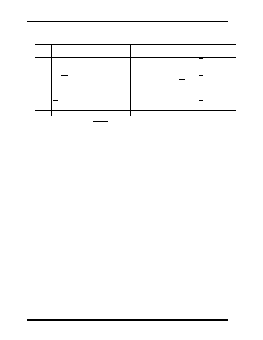
T
CE
Chip-Enable Access Time
--
230
450
nsec
CS or CE, RD = LOW (Note 1)
T
RE
Read-Enable Access Time
--
190
450
nsec
CS = HIGH, CE = LOW, (Note 1)
T
DHC
Data Hold From CS or CE
--
250
450
nsec
RD = LOW, (Note 1)
T
DHR
Data Hold From RD
--
210
450
nsec
CS = HIGH, CE = LOW, (Note 1)
T
OP
OVR/POL Data Access Time
--
140
300
nsec
CS = HIGH, CE = LOW,
RD = LOW, (Note 1)
T
LH
Low/High Byte Access Time
--
140
300
nsec
CS = HIGH, CE = LOW,
RD = LOW, (Note 1)
Clock Setup Time
100
--
--
nsec
Positive or Negative Pulse Width
T
WRE
RD Minimum Pulse Width
450
230
--
nsec
CS = HIGH, CE = LOW, (Note 2)
T
WRD
RD Minimum Delay Time
150
50
--
nsec
CS = HIGH, CE = LOW, (Note 2)
T
WWD
WR Minimum Pulse Width
75
25
--
nsec
CS = HIGH, CE = LOW, (Note 1)
TC850 ELECTRICAL SPECIFICATIONS (CONTINUED)
Electrical Characteristics: V
S
= ±5V; F
CLK
= 61.44kHz, V
FS
= 3.2768V, T
A
= 25°C, Figure 1-1, unless otherwise specified.
Symbol
Parameter
Min
Typ
Max
Unit
Test Conditions
Note
1:
Demand mode, CONT/DEMAND = LOW. Figure 8-5 timing diagram. C
L
= 100pF.
2:
Continuous mode, CONT/DEMAND = HIGH. Figure 8-7 timing diagram.
3:
Digital inputs have CMOS logic levels and internal pull-up/pull-down resistors. For TTL compatibility, external pull-up
resistors to V
DD
are recommended.
©
2002 Microchip Technology Inc.
DS21479B-page 5
TC850
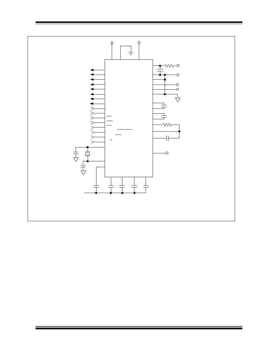
FIGURE 1-1:
STANDARD TEST CIRCUIT CONFIGURATION
V
DD
V
SS
16
8
9
10
11
12
13
14
15
1
2
3
4
5
6
7
17
TC850
0.01
µF Input
+1.6384V
+0.0256V
100M
120Mk
1
µF*
1
µF*
0.1
µF
0.1
µF
0.1
µF
0.1
µF
0.1
µF
0.1
µF
BUFFER
OSC
1
OSC
2
INT
IN
INT
OUT
C
INTB
C
BUFA
C
BUFB
C
INTA
R
INT
C
INT
COMP
TEST
NC
18
21
28
27
29
26
19
23
24
25
35
34
37
38
36
33
39
30
31
61.44 kHz
20
22
40
-5V
+5V
DGND
32
**
**
NOTES: Unless otherwise specified, all 0.1
µF capacitors are film dielectric.
Ceramic capacitors are not recommended.
NC = No Connection
*Polypropylene
capacitors.
** 100pF Mica capacitors.
DB0
DB1
DB2
DB3
DB4
DB5
DB6
DB7
BUSY
CS
CE
WR
RD
CONT/DEMAND
OVR/POL
L/H
IN-
IN+
REF-
ANALOG COMMON
REF
1
+
REF
2
+
C
REF1
+
C
REF1
-
C
REF2
-
C
REF2
+