 | –≠–ª–µ–∫—Ç—Ä–æ–Ω–Ω—ã–π –∫–æ–º–ø–æ–Ω–µ–Ω—Ç: TCM1617 | –°–∫–∞—á–∞—Ç—å:  PDF PDF  ZIP ZIP |
1
TCM1617
TCM1617-1 2/5/99
2001 Microchip Technology Inc. DS21485A
SMBus Thermal Sensor with External Diode Input
FEATURES
s
Includes Internal External Sensing Capability
s
Outputs Temperature as 8-Bit Digital Word
s
Solid State Temperature Sensing; 1
∞
C Resolution
s
3.0 ≠ 5.5V Operating Range
s
Independent Internal and External Threshold
Set-Points With ALERT# Interrupt Output
s
SMBus 2-Wire Serial Interface
s
Up To Nine TCM1617s May Share the Same Bus
s
Standby Mode for Low Standby Power
s
Low Power ............................ 70
µ
A (max) Operating
...................................... 10
µ
A (max) Standby Mode
s
16-Pin Plastic QSOP Package
TYPICAL APPLICATIONS
s
Thermal Protection For Intel "Deschutes"
Pentium IITM and Other High Performance CPUs
with Integrated On-Board Diode -- No Sensor
Mounting Problems!
s
Accurate Thermal Sensing From Any Si Junction
Diode
s
Thermal Management in Electronic Systems:
Computers, Network Equipment, Power Supplies
GENERAL DESCRIPTION
The TCM1617 is a serially programmable temperature
sensor optimized for monitoring modern high performance
CPUs with on-board integrated thermal diodes. Tempera-
ture data is converted from the CPU's thermal diode outputs
and made available as an 8-Bit digital word.
Communication with the TCM1617 is accomplished via
the standard System Management Bus (SMBus) commonly
used in modern computer systems. This permits reading the
current internal/external temperature, programming the
threshold setpoints, and configuring the device. Addition-
ally, an interrupt is generated on the ALERT# pin when
temperature moves outside the preset threshold windows in
either direction.
A Standby command may be sent via the SMBus by
signaling the STBY# input to activate the low-power Standby
mode. Registers can be accessed while in Standby mode.
Address selection inputs allow up to nine TCM1617s to
share the same 2-wire SMBus for multi-zone monitoring.
All registers can be read by the host, and both polled and
interrupt driven systems are easily accommodated. Small
size, low installed cost, and ease of use make the TCM1617
an ideal choice for implementing sophisticated system man-
agement schemes, such as ACPI.
ORDERING INFORMATION
Part No.
Package
Temp. Range
TCM1617MQR
QSOP-16
≠55
∞
C to +125
∞
C
TCM1617EV
Evaluation Kit for TCM1617
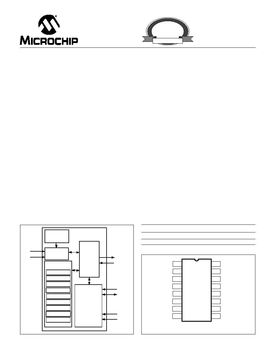
BLOCK DIAGRAM
PIN CONFIGURATION
EVALUATION
KIT
AVAILABLE
Register Set
Modulator
Control
Logic
SMBus
Interface
ALERT#
STBY#
SCL
SDA
ADD 0
ADD 1
D
+
D
≠
Ext. Temp
Status Byte
Config. Byte
Conv. Rate
Ext. Hi Limit
Ext. Lo Limit
Int. Hi Limit
Int. Lo Limit
Int. Temp
Internal
Sensor
(Diode)
16-Pin Plastic QSOP
1
16
2
15
3
14
4
13
5
12
6
11
7
10
NC
D≠
8
9
V
DD
NC
GND
GND
SCL
STBY#
NC
SDA
ALERT#
ADD0
NC
D+
TCM1617
NC
ADD 1

2
SMBus Thermal Sensor with External Diode Input
TCM1617
TCM1617-1 2/5/99
2001 Microchip Technology Inc. DS21485A
ABSOLUTE MAXIMUM RATINGS*
Power Supply Voltage (V
DD
) ......................................... 6V
Voltage On Any Pin ............ (GND ≠ 0.3V) to (V
DD
+ 0.3V)
Operating Temperature (T
A
) .................. ≠55
∞
C to +125
∞
C
Storage Temperature (T
STG
) .................. ≠65
∞
C to +150
∞
C
SMBus Input/Output Current ................. ≠1 mA to +50 mA
D≠ Input Current ......................................................
±
1 mA
Max. Power Dissipation ........................................330 mW
*Static-sensitive device. Unused devices must be stored in conductive
material. Protect devices from static discharge and static fields. Stresses
above those listed under Absolute Maximum Ratings may cause perma-
nent damage to the device. These are stress ratings only and functional
operation of the device at these or any other conditions above those
indicated in the operational sections of the specifications is not implied.
Exposure to Absolute Maximum Rating Conditions for extended periods
may affect device reliability.
ELECTRICAL CHARACTERISTICS:
V
DD
= 3.3V, ≠55
∞
C
T
A
125
∞
C, unless otherwise noted.
Symbol
Parameter
Test Conditions
Min
Typ
Max
Unit
Power Supply
V
DD
Power Supply Voltage
≠55
T
A
+125
∞
C
3.0
--
5.5
V
V
UV-LOCK
V
DD
Undervoltage
2.4
2.80
2.95
V
Lockout Threshold
V
POR
Power-On Reset Threshold
V
DD
Falling Edge
1.0
1.7
2.3
V
I
DD
Operating Current
0.25 Conv./Sec Rate
--
--
70
µ
A
SMBus Inactive (Note 1)
I
DD
Operating Current
2 Conv./Sec Rate
--
--
180
µ
A
SMBus Inactive (Note 1)
I
DD-STANDBY
Standby Supply Current
V
DD
= 3.3V SMBus Active
--
--
100
µ
A
I
DD-STANDBY
Standby Supply Current
V
DD
= 3.3V, SMBus Inactive
--
--
10
µ
A
I
ADD-BIAS
ADD[1:0] Bias Current
Power-Up Only
--
160
--
µ
A
ALERT# Output
V
OL
Output Low Voltage
I
OL
= 1.0 mA (Note 3)
--
--
0.4
V
ADD[1:0] Inputs
V
IL
Logic Input Low
--
--
V
DD
x 0.3
V
V
IH
Logic Input High
V
DD
x 0.7
--
--
V
STBY# Input
V
IL
Logic Input Low
--
--
V
DD
x 0.3
V
V
IH
Logic Input High
V
DD
x 0.7
--
--
V
Temp-to-Bits Converter
T
RES
Basic Temperature Resolution
--
1
--
∞
C
T
IERR1
Internal Diode Temperature
+60
∞
C
T
A
+100
∞
C
≠2
--
+2
∞
C
0
∞
C
T
A
+125
∞
C
≠3
--
+3
∞
C
≠55
∞
C
T
A
< 0
∞
C
--
±
3
--
T
EERR
External Diode Temperature
+60
∞
C
T
A
+100
∞
C
≠3
--
+3
∞
C
(Note 4)
0
∞
C
T
A
+125
∞
C ≠3
≠5
--
+5
∞
C
≠55
∞
C
T
A
< 0
∞
C
±
5
--
∞
C
I
DIODE-HIGH
External Diode
(D+) ≠ (D≠) ~ 0.65V
--
100
--
µ
A
High Source Current
I
DIODE-LOW
External Diode
(D+) ≠ (D≠) ~ 0.65V
--
10
--
µ
A
Low Source Current
V
D-SOURCE
D≠ Source Voltage
--
0.7
--
V

3
TCM1617
TCM1617-1 2/5/99
2001 Microchip Technology Inc. DS21485A
SMBus Thermal Sensor with External Diode Input
NOTES: 1. Operating current is an average value (including external diode injection pulse current) integrated over multiple conversion cycles.
Transient current may exceed this specification.
2. For true reccurring conversion time see Conversion Rate register description.
3. Output current should be minimized for best temperature accuracy. Power dissipation within the TCM1617 will cause self-heating and
temperature drift error.
4. Refer to Application Note 64.
SMBus PORT AC TIMING:
V
DD
= 3.3V, ≠55
(T
A
= T
J
)
125
∞
C; C
L
= 80 pF, unless otherwise noted.
Symbol
Parameter
Test Conditions
Min
Typ
Max
Unit
f
SMB
SMBus Clock Frequency
10
--
100
KHz
t
LOW
Low Clock Period
10% to 10%
4.7
--
--
µ
sec
t
HIGH
High Clock Period
90% to 90%
4
--
--
µ
sec
t
R
SMBus Rise Time
10% to 90%
--
--
1,000
nsec
t
F
SMBus Fall Time
90% to 10%
--
--
300
nsec
t
SU(START)
Start Condition Setup Time
90% SCL to 10% SDA
4
--
--
µ
sec
(for Repeated Start Condition)
t
H(START)
Start Condition Hold Time
4
--
--
µ
sec
t
SU-DATA
Data in Set Up Time
1000
--
--
nsec
t
H-DATA
Data in Hold Time
1250
--
--
nsec
t
SU(STOP)
Stop Condition Setup Time
4
--
--
µ
sec
t
IDLE
Bus Free Time Prior to
4.7
--
--
µ
sec
New Transition
Symbol
Parameter
Conditions
Min
Typ
Max
Unit
t
CONV
Conversion Time
from CHIP STOP to Conv.
54
83
112
msec
Complete (Note 2)
CR
Conversion Rate Accuracy
See Conversion Rate Register Desc.
≠35
--
+35
%
2-Wire SMBus Interface
V
IH
Logic Input High
2.2
--
--
V
V
IL
Logic Input Low
--
--
0.8
V
V
OL
SDA Output Low
I
OL
= 2 mA (Note 3)
--
--
0.4
V
I
OL
= 4 mA (Note 3)
--
--
0.6
V
C
IN
Input Capacitance SDA, SCL
--
5
--
pF
I
LEAK
I/O Leakage
≠1
0.1
1
µ
A
ELECTRICAL CHARACTERISTICS (CONT):
V
DD
= 3.3V, ≠55
∞
C
T
A
125
∞
C, unless otherwise noted.
4
SMBus Thermal Sensor with External Diode Input
TCM1617
TCM1617-1 2/5/99
2001 Microchip Technology Inc. DS21485A
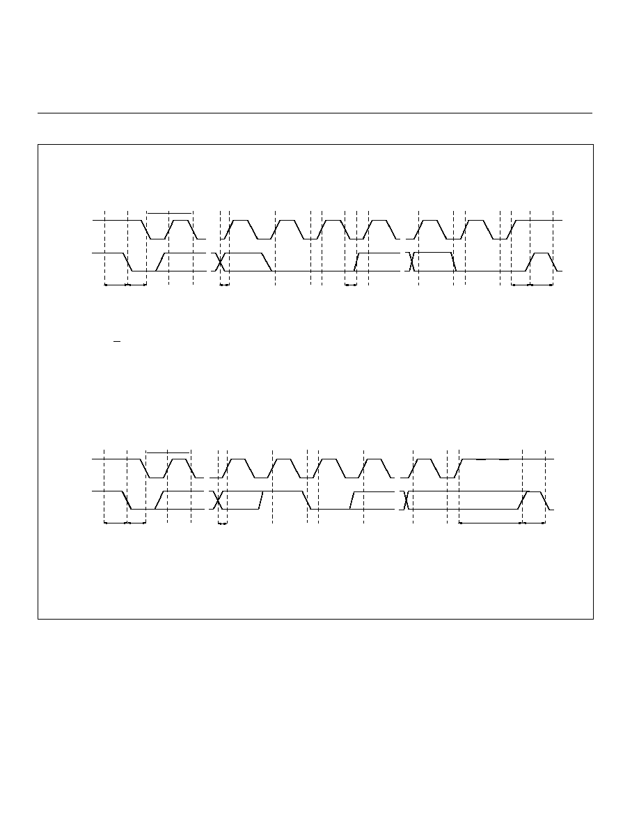
SMBUS Write Timing Diagram
SMBUS Read Timing Diagram
SMBUS THERMAL S
tSU(START) tH(START)
tSU-DATA
tH-DATA
tSU(STOP) tIDLE
A = Start Condition
B = MSB of Address Clocked into Slave
C = LSB of Address Clocked into Slave
D = R/W Bit Clocked into Slave
E = Slave Pulls SDA Line Low
A
B
C
D
E
F
G
H
I
J
K
L
M
F = Acknowledge Bit Clocked into Master
G = MSB of Data Clocked into Slave
H = LSB of Data Clocked into Slave
I = Slave Pulls SDA Line Low
J = Acknowledge Clocked into Master
K = Acknowledge Clock Pulse
L = Stop Condition, Data Executed by Slave
M = New Start Condition
ILOW
IHIGH
SCL
SDA
tSU(START)
tH(START)
tSU-DATA
tSU(STOP)
tIDLE
A = Start Condition
B = MSB of Address Clocked into Slave
C = LSB of Address Clocked into Slave
D = R/W Bit Clocked into Slave
A
B
C
D
E
F
G
H
I
J
K
E = Slave Pulls SDA Line Low
F = Acknowledge Bit Clocked into Master
G = MSB of Data Clocked into Master
H = LSB of Data Clocked into Master
ILOW
IHIGH
I = Acknowledge Clock Pulse
J = Stop Condition
K = New Start Condition
SCL
SDA

5
TCM1617
TCM1617-1 2/5/99
2001 Microchip Technology Inc. DS21485A
SMBus Thermal Sensor with External Diode Input
PIN DESCRIPTION
Pin Number
Symbol
Type
Description
2
V
DD
Power
Power Supply Input
3
D+
Bi-Directional
Current Source and A/D Positive Input
4
D≠
Bi-Directional
Current Sink and A/D Negative Input
6,10
ADD[1:0]
Input
Address Select Pins (See Address Decode Table)
7,8
GND
Power
System Ground
11
ALERT#
Output
SMBus Interrupt (SMBALERT#)
12
SDA
Bi-Directional
SMBus Serial Data
14
SCL
Input
SMBus Serial Clock
15
STBY#
Input
Standby Enable
1,5, 9, 13,16
NC
--
Not Connected
PIN DESCRIPTION
SCL
Input. SMBus serial clock. Clocks data into and out of
the TCM1617. See System Management Bus Specification,
rev. 1.0, for timing diagrams.
SDA
Bi-directional. Serial data is transferred on the SMBus
in both directions using this pin. See System Management
Bus Specification, rev. 1.0, for timing diagrams.
ADD1, ADD0
Inputs.
Sets the 7-bit SMBus address. These pins are
"tri-state," and the SMBus addresses are specified in the
Address Decode Table below.
(NOTE: The tri-state scheme allows up to nine
TCM1617s on a single bus. A match between the TCM1617's
address and the address specified in the serial bit stream
must be made to initiate communication. Many SMBus-
compatible devices with other addresses may share the
same 2-wire bus (see System Management Bus Specifica-
tion rev. 1.0 for address allocations). These pins are only
active at power-on reset, and will latch into the appropriate
states.
ALERT#
Output, Open Collector, Active Low. The ALERT# out-
put corresponds to the general SMBALERT# signal and
indicates an interrupt event. The TCM1617 will respond to
the standard SMBus Alert Response Address (see SMBus
Specification 1.0) and associated protocol when ALERT# is
asserted. Normally, the ALERT# output will be asserted
when any of the following occurs:
INT_TEMP equal to or exceeds INT_HLIM
INT_TEMP falls below INT_LLIM
EXT_TEMP equal to or exceeds EXT_HLIM
EXT_TEMP falls below EXT_LLIM
External Diode "Open"
The operation of the ALERT# output is controlled by the
MASK1 bit in the CONFIG register. If the MASK1 bit is set to
"1," no interrupts will be generated on ALERT#. The ALERT#
output is cleared and re-armed by the Alert Response
Address (ARA). This output may be WIRE-ORed with simi-
lar outputs from other SMBus devices. If the alarm condition
persists after the ARA, the ALERT# output will be immedi-
ately re-asserted.
(NOTE: A pull-up resistor is necessary on ALERT#
since it is an open-drain output. Current sourced from the
pull-up resistor causes power dissipation and may cause
internal heating of the TCM1617. To avoid affecting the
accuracy of internal temperature readings, the pull-up resis-
tors should be made as large as possible.)
STBY#
Input. The activation of Standby mode may be achieved
using either the STBY# pin or the CHIP STOP bit (CONFIG
register). If STBY# is pulled low, the TCM1617 uncondition-
ally enters its low-power Standby mode (I
DD
= 10
µ
A, max).
The temperature-to-digital conversion process is halted, but
ALERT remains functional. The TCM1617's bus interface

6
SMBus Thermal Sensor with External Diode Input
TCM1617
TCM1617-1 2/5/99
2001 Microchip Technology Inc. DS21485A
Standby Mode Operation
STBY#
Chip Stop Bit
One Shot?
Operating Mode
0
Don't Care
Don't Care
Standby
1
0
Don't Care
Normal
1
1
No
Standby
1
1
Yes
Normal
(1 Conversion Only,
then Standby)
remains active, and all registers may be read from and
written to normally. The INT_TEMP and EXT_TEMP regis-
ters will contain whatever data was valid at the time of
Standby. (Transitions on SDA or SCL due to external bus
activity may increase the Standby power consumption.)
D+
Bi-directional. this pin connects to the anode of the
external diode and is the positive A/D input. Current is
injected into the external diode from the TCM1617, and the
temperature proportional V
BE
is measured and converted to
digital temperature data.
D≠
Bi-directional. This pin connects to the cathode of the
external diode. Current is sunk from the external diode into
the TCM1617 through this pin. It also is the negative input
terminal to the TCM1617's A/D converter. This node is kept
at approximately 0.7V above GROUND.
V
DD
Input. Power supply input. See electrical specifications.
GND
Input. Ground return for all TCM1617 functions.
FUNCTIONAL DESCRIPTION
The TCM1617 acquires and converts temperature infor-
mation from two separate sources, both silicon junction
diodes, with a basic accuracy of
±
1
∞
C. One is located on the
TCM1617 die; the other is connected externally. The exter-
nal diode may be located on another IC die. The analog-to-
digital converter on the TCM1617 alternately converts tem-
perature data from the two sensors and stores them sepa-
rately in internal registers.
The system interface is a slave SMBus port with an
ALERT# (SMBALERT#) interrupt output. The interrupt is
triggered when one or more of four preset temperature
thresholds are tripped (see Figure 1). These four thresholds
are user-programmable via the SMBus port. Additionally,
the temperature data can be read at any time through the
SMBus port. Nine SMBus addresses are programmable for
the TCM1617, which allows for a multi-sensor configuration.
Also, there is low-power Standby mode where temperature
acquisition is suspended.
STANDBY MODE
The TC1617 allows the host to put it into a low power
mode (I
DD
= 10
µ
A, max) Standby mode. In this mode, the
A/D converter is halted, and the temperature data registers
are frozen. The SMBus port operates normally. Standby
mode can be enabled with either the STBY# input pin or the
CHIP STOP bit in the CONFIG register. The following table
summarizes this operation.
Figure 1. Temperature-vs-Setpoint Event Generation
SMBUS SLAVE ADDRESS
The two pins ADD1 and ADD0 are tri-state input pins
which determine the 7-Bit SMBus slave address of the
TCM1617. The address is latched during POR.
SERIAL PORT OPERATION
Temperature
Setpoints
Time
EXT_HLIM
INT_HLIM
EXT_LLIM
INT_LLIM
EXT_TEMP
INT_TEMP
ASSERT
ALERT#
ALERT#
ASSERT
ALERT#
ASSERT
ALERT#
ASSERT
ALERT#
Note: This diagram inplies that the appropriate setpoint is moved, temporarily, after each ALERT#
event to suppress re-assertion of ALERT# immediately after the ARA/de-assertion.
7
TCM1617
TCM1617-1 2/5/99
2001 Microchip Technology Inc. DS21485A
SMBus Thermal Sensor with External Diode Input
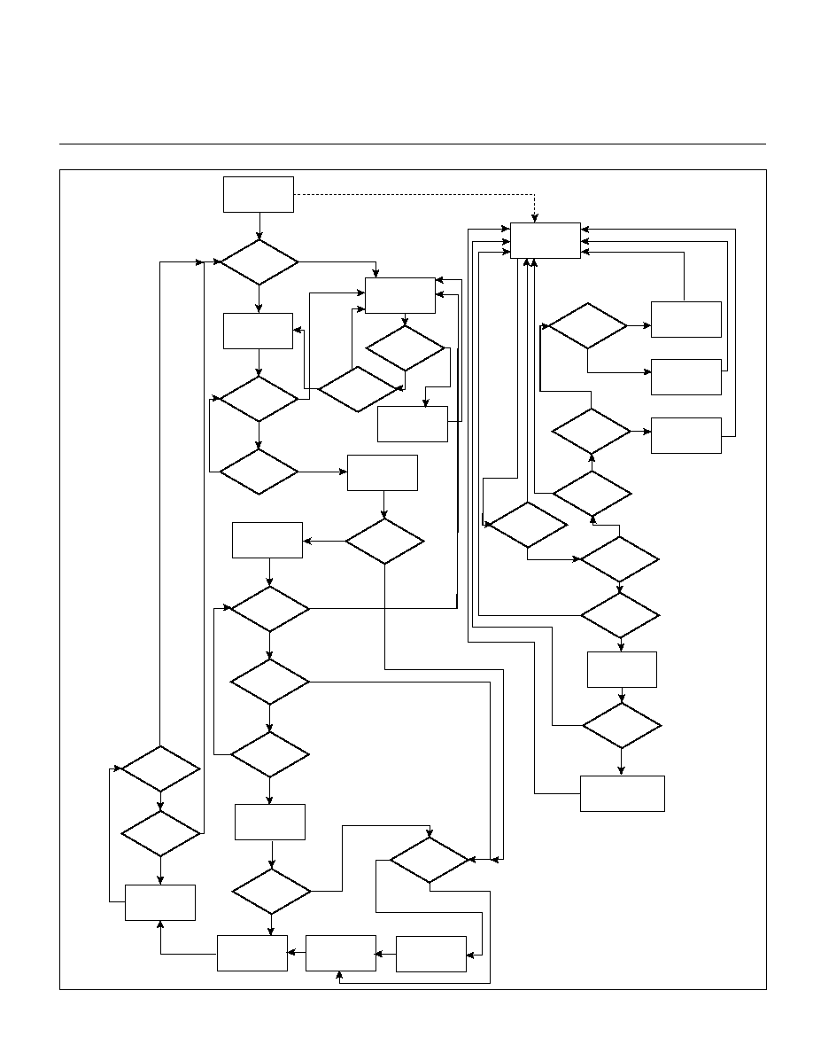
Figure 2. TCM1617 Functional Description Flowchart
NO
NO
NO
YES
STBY mode
active?
YES
NO
NO
POR, initialize
all registers
NO
YES
YES
YES
YES
Start internal
conversion,
STATUS [D7]
STBY
active?
EOC?
Monitor SMBus
for START
condition
Stop conv., reset
STATUS D[7]
Update
INT_TEMP
Thermal Trip?
Start external
conversion
STBY
active?
NO
Ext. diode
open?
EOC?
YES
Update
EXT_TEMP
Thermal Trip?
YES
CONFIG
[D7] active?
YES
NO
Enable
ALERT#
NO
Set appropriate
STATUS bit
D[6:2]
Reset STATUS
bit D[7]
YES
NO
Execute
STATUS read and
clear STATUS
Execute SMBus
read
Execute SMBus
write
STATUS
read?
Read/
Write?
ARA?
ALERT#
active?
Disable and re-arm
ALERT#, send
local address to host
YES
WRITE
YES
READ
YES
YES
NO
One Shot?
Rest
period over?
YES
NO
NO
YES
NO
NO
NO
Perform one
conversion cycle
STBY
released?
One
shot?
YES
NO
Valid
command?
ARA bus
arbitration
Win
arbitration?
YES
YES
Address
match?
NO
NO
Rest Period
according to
CONV_RATE
register

8
SMBus Thermal Sensor with External Diode Input
TCM1617
TCM1617-1 2/5/99
2001 Microchip Technology Inc. DS21485A
Address Decode Table
ADD0
ADD1
SMBus Address
0
0
0011 000
0
open (3-state)
0011 001
0
1
0011 010
open (3-state)
0
0101 001
open (3-state)
(open (3-state)
0101 010
open (3-state)
1
0101 011
1
0
1001 100
1
open (3-state)
1001 101
1
1
1001 110
The Serial Clock input (SCL) and bi-directional data port
(SDA) form a 2-wire bi-directional serial port for program-
ming and interrogating the TCM1617. The following conven-
tions are used in this bus architecture:
All transfers take place under control of a host, usually
a CPU or microcontroller, acting as the Master, which
provides the clock signal for all transfers. The TCM1617
always operates as a slave. The serial protocol is illustrated
in Figure 3. All data transfers have two phases; all bytes are
transferred MSB first. Accesses are initiated by a start
condition (START), followed by a device address byte and
TCM1617 Serial Bus Conventions
Term
Explanation
Transmitter
The device sending data to the bus.
Receiver
The device receiving data from the bus.
Master
The device which controls the bus: initiating
transfers (START), generating the clock, and
terminating transfers (STOP).
Slave
The device addressed by the master.
Start
A unique condition signaling the beginning of
a transfer indicated by SDA falling (High ≠ Low)
while SCL is high.
Stop
A unique condition signaling the end of a
transfer indicated by SDA rising (Low ≠ High)
while SCL is high.
ACK
A receiver acknowledges the receipt of each
byte with this unique condition. The receiver
drives SDA low during SCL high of the ACK
clock-pulse. The Master provides the clock
pulse for the ACK cycle.
Busy
Communication is not possible because the
bus is in use.
NOT Busy
When the bus is idle, both SDA and SCL
will remain high.
Data Valid
The state of SDA must remain stable during
the High period of SCL in order for a data bit to
be considered valid. SDA only changes state
while SCL is low during normal data transfers
(see Start and Stop conditions.)
one or more data bytes. The device address byte includes
a Read/Write selection bit. Each access must be terminated
by a Stop Condition (STOP). A convention called (ACK)
confirms receipt of each byte. Note that SDA can change
only during periods when SCL is LOW (SDA changes while
SCL is High are reserved for Start and Stop conditions.)
Start Condition (START)
The TCM1617 continuously monitors the SDA and SCL
lines for a start condition (a High to Low transition of SDA
while SCL is High), and will not respond until this condition
is met.
Address Byte
Immediately following the Start Condition, the host must
transmit the address byte to the TCM1617. The states of
ADD1 and ADD0 during power-up determine the 7-bit
SMBus address for the TCM1617. The 7-bit address trans-
mitted in the serial bit stream must match for the TCM1617
to respond with an Acknowledge (indicating the TCM1617 is
on the bus and ready to accept data). The eighth bit in the
Address Byte is a Read-Write Bit. This bit is 1 for a read
operation or 0 for a write operation.
Acknowledge (ACK)
Acknowledge (ACK) provides a positive handshake
between the host and the TCM1617. The host releases SDA
after transmitting eight bits, then generates a ninth clock
cycle to allow the TCM1617 to pull the SDA line Low to
acknowledge that it successfully received the previous eight
bits of data or address.
Data Byte
After a successful ACK of the address byte, the host
must next transmit the data byte to be written or clock out the
data to be read. (See the appropriate timing diagrams.) ACK
will be generated after a successful write of a data byte into
the TCM1617.

9
TCM1617
TCM1617-1 2/5/99
2001 Microchip Technology Inc. DS21485A
SMBus Thermal Sensor with External Diode Input
Figure 3. SMBus Protocols
S
ADDRESS
WR
ACK
COMMAND
ACK
DATA
ACK
P
8 Bits
7 Bits
8 Bits
Slave Address
Command Byte: selects
which register you are
writing to.
Data Byte: data goes
into the register set
by the command byte.
Write Byte Format
Read Byte Format
S
ADDRESS WR
ACK
COMMAND
ACK
S
ADDRESS
RD
ACK
DATA
NACK P
7 Bits
8 Bits
7 Bits
8 Bits
Slave Address
Command Byte: selects
which register you are
reading from.
Slave Address: repeated
due to change in data-
flow direction.
Data Byte: reads from
the register set by the
command byte.
Receive Byte Format
S
ADDRESS
RD
ACK
DATA
NACK P
7 Bits
8 Bits
Data Byte: reads data from
the register commanded by
the last Read Byte.
S = Start Condition
P = Stop Condition
Shaded = Slave Transmission
Send Byte Format
S
ADDRESS WR
ACK
COMMAND
ACK
P
7 Bits
8 Bits
Command Byte: sends
command with no data,
usually used for one-shot
command.

10
SMBus Thermal Sensor with External Diode Input
TCM1617
TCM1617-1 2/5/99
2001 Microchip Technology Inc. DS21485A
Stop Condition (STOP)
Communications must be terminated by a stop condi-
tion (a Low to High transition of SDA while SCL is High). The
Stop Condition must be communicated by the transmitter to
the TCM1617. (Refer to TCN75 data sheet for serial bus
timing diagrams.)
REGISTER SET AND PROGRAMMER'S
MODEL
TCM1617 Command Set
The TCM1617 supports four SMBus command proto-
cols. These are READ_BYTE, WRITE_BYTE, SEND_BYTE,
and RECEIVE_BYTE. See System Management Bus Speci-
fication Rev. 1.0 for details.
Command Byte Description
Command
Code
Function
RIT
00h
Read Internal Temp (INT_TEMP)
RET
01h
Read External Temp (EXT_TEMP)
RS
02h
Read Status Byte (STATUS)
RC
03h
Read Configuration Byte (CONFIG)
RCR
04h
Read Conversion Rate Byte
(CONV_RATE)
RIHL
05h
Read Internal High Limit
(INT_HLIM)
RILL
06h
Read Internal Low Limit (INT_LLIM)
REHL
07h
Read External High Limit
(EXT_HLIM)
RELL
08h
Read External Low Limit
(EXT_LLIM)
WC
09h
Write Configuration Byte (CONFIG)
WCR
0Ah
Write Conversion Rate Byte
(CONV_RATE)
WIHL
0Bh
Write Internal High Limit
(INT_HLIM)
WILL
0Ch
Write Internal Low Limit (INT_LLIM)
WEHL
0Dh
Write External High Limit
(EXT_HLIM)
WELL
0Eh
Write External Low Limit
(EXT_LLIM)
OSHT
0Fh
One Shot Temp Measurement
RMID
FEh
Read Manufacturer ID (MFR_ID)
RMREV
FFh
Read Manufacturer Revision
Number (MFR_REV)
Configuration Register (Config), 8-Bits,
Read/Write
Configuration Register (Config)
D[7]
D[6]
D[5]
D[4]
D[3]
D[2]
D[1]
D[0]
Mask1 Chip Stop
Reserved
Bit
POR State Function
Operation
D[7]
0
Interrupt Mask
1 = mask ALERT#,
(see text)
0 = don't mask
ALERT #
D[6]
0
Standby switch
1 = standby,
0 = normal
D[5] ≠ D[0]
0
Reserved ≠
N/A
Always returns
zero when read.
A/D Conversion Rate Register
(CONV_RATE), 8-Bits, Read/Write
A/D Conversion Rate Register (CONV_RATE)
D[7]
D[6]
D[5]
D[4]
D[3]
D[2]
D[1]
D[0]
Reserved
MSB
X
LSB
Bit
POR State Function
Operation
D[7:3]
0
Reserved ≠ Always
N/A
returns zero when
read.
D[2:0]
010b
Conversion rate bits.
See below.
A/D Conversion Rate Selection
D2
D1
D0
Conversion Rate
Sa/sec
0
0
0
0.0625
0
0
1
0.125
0
1
0
0.25
0
1
1
0.5
1
0
0
1.0
1
0
1
2.0
1
1
0
4.0
1
1
1
8.0
NOTE: Conversion rate denotes actual sampling of both internal
and
external sensors.
NOTE: Proper device operation is NOT guaranteed if undefined locations
(10h to FDh) are addressed. In case of erroneous SMBus operation
(RECEIVE_BYTE command issued immediately after
WRITE_BYTE command) the TCM1617 will ACKnowledge the
address and return 1111 1111b to signify an error. Under no
condition will it implement an SMBus "timeout."
11
TCM1617
TCM1617-1 2/5/99
2001 Microchip Technology Inc. DS21485A
SMBus Thermal Sensor with External Diode Input
Temperature Registers, 8-Bits, Read-Only
(INT_TEMP, EXT_TEMP)
The binary value (2's complement format) in these two
registers represents temperature of the internal and external
sensors following a conversion cycle. The registers are
automatically updated in an alternating manner.
Internal Temperature Register (INT_TEMP)
D[7]
D[6]
D[5]
D[4]
D[3]
D[2]
D[1]
D[0]
MSB
x
x
x
x
x
x
LSB
External Temperature Register (EXT_TEMP)
D[7]
D[6]
D[5]
D[4]
D[3]
D[2]
D[1]
D[0]
MSB
x
x
x
x
x
x
LSB
Temperature Threshold Setpoint Registers,
8-Bits, Read-Write (INT_HLIM, INT_LLIM,
EXT_HLIM, EXT_LLIM)
These registers store the values of the upper and lower
temperature setpoints for event detection. The value is in
2's-complement binary. INT_HLIM and INT_LLIM are com-
pared with the INT_TEMP value, and EXT_HLIM and
EXT_LLIM are compared with EXT_TEMP. These registers
may be written at any time.
Internal High Limit Setpoint Register (INT_HLIM)
D[7]
D[6]
D[5]
D[4]
D[3]
D[2]
D[1]
D[0]
MSB
x
x
x
x
x
x
LSB
Internal Low Limit Setpoint Register (INT_LLIM)
D[7]
D[6]
D[5]
D[4]
D[3]
D[2]
D[1]
D[0]
MSB
x
x
x
x
x
x
LSB
External High Limit Setpoint Register (EXT_HLIM)
D[7]
D[6]
D[5]
D[4]
D[3]
D[2]
D[1]
D[0]
MSB
x
x
x
x
x
x
LSB
External Low Limit Setpoint Register (EXT_LLIM)
D[7]
D[6]
D[5]
D[4]
D[3]
D[2]
D[1]
D[0]
MSB
x
x
x
x
x
x
LSB
NOTE: POR states:
INT_HLIM
01111111b
+127
∞
C
INT_LLIM
11001001b
≠55
∞
C
EXT_HLIM
01111111b
+127
∞
C
EXT_LLIM
11001001b
≠55
∞
C
In the two temperature data and four threshold setpoint
registers, each unit value represents one degree (Celsius).
The value is in 2's-complement binary format such that a
reading of 00000000b corresponds to 0
∞
C. Examples of this
temperature-to-binary value relationship are shown in the
following table.
Temperature-to-Digital Value Conversion
(INT_TEMP, EXT_TEMP, INT_HLIM, INT_LLIM,
EXT_HLIM, EXT_LLIM)
Actual
Rounded
Binary
Hex
Temperature
Temperature
Value
Value
+130.00
∞
C
+127
∞
C
01111111
7F
+127.00
∞
C
+127
∞
C
01111111
7F
+126.50
∞
C
+127
∞
C
01111111
7F
+25.25
∞
C
+25
∞
C
00011001
19
+0.50
∞
C
+1
∞
C
00000001
01
+0.25
∞
C
0
∞
C
00000000
00
0.00
∞
C
0
∞
C
00000000
00
≠0.25
∞
C
0
∞
C
00000000
00
≠0.50
∞
C
0
∞
C
00000000
00
≠0.75
∞
C
≠1
∞
C
11111111
FF
≠1.00
∞
C
≠1
∞
C
11111111
FF
≠25.00
∞
C
≠25
∞
C
11100111
E7
≠25.25
∞
C
≠25
∞
C
11100110
E7
≠54.75
∞
C
≠55
∞
C
11001001
C9
≠55.00
∞
C
≠55
∞
C
11001001
C9
≠65.00
∞
C
≠65
∞
C
10111111
BF
12
SMBus Thermal Sensor with External Diode Input
TCM1617
TCM1617-1 2/5/99
2001 Microchip Technology Inc. DS21485A
Status Register (Status), 8-Bits, Read Only:
Status Register (Status)
D[7]
D[6]
D[5]
D[4]
D[3]
D[2]
D[1]
D[0]
Busy
Flag1
Flag2
Flag3
Flag4
Flag5 Reserved
Bit
POR
Function
Operation*
State
D[7]
0
Signal A/D
1 = A/D busy,
converter is busy.
0 = A/D idle
D[6]
0
Interrupt flag for
1 = interrupt occurred,
INT_HLIM event
0 = none
D[5]
0
Interrupt flag for
1 = interrupt occurred,
INT_LLIM event
0 = none
D[4]
0
Interrupt flag for
1 = interrupt occurred,
EXT_HLIM event
0 = none
D[3]
0
Interrupt flag for
1 = interrupt occurred,
EXT_LLIM event
0 = none
D[2]
0
External diode
1 = external diode fault,
"fault" flag
0 = external diode OK
D[1:0]
0
Reserved ≠
N/A
Always
returns zero.
NOTE: All status bits are cleared after a read operation is performed on
STATUS. The EXT_TEMP register will read +127
∞
C if an external
diode "open" is detected.
Name
Description
POR
Read Write
State
INT_TEMP
Internal sensor
0000 0000b*
temperature
(2's complement)
EXT_TEMP
External sensor
0000 0000b*
temperature
(2's complement)
STATUS
STATUS register
0000 0000b
CONFIG
CONFIG register
0000 0000b
CONV_RATE A/D conversion
0000 0010b
rate register
INT_HLIM
Internal high
0111 1111b
limit
(2's complement)
INT_LLIM
Internal low
1100 1001b
limit
(2's complement)
EXT_HLIM
External high
0111 1111b
limit
(2's complement)
EXT_LLIM
External low
1100 1001b
limit
(2's complement)
MFR_ID
ASCII for letter "T" 0101 0100b
(Microchip)
MFR_REV
Serial device
**
revision#
NOTE: *The INT_TEMP and EXT_TEMP register immediately will be
updated by the A/D converter after POR. If STBY# is low at power-
up, INT_TEMP and EXT_TEMP will remain in POR state (0000
0000b). **MFR_REV will sequence 01h, 02h, 03h, etc. by mask-
ing changes.
The TCM1617's register set is summarized below. All
registers are 8-bits wide.
Manufacturer's Identification Register (MFR_ID)
D[7]
D[6]
D[5]
D[4]
D[3]
D[2]
D[1]
D[0]
MSB
X
X
X
X
X
X
LSB
Manufacturer's Identification Register
(MFR_ID), 8-Bits, Read Only:
Manufacturer's Revision Register (MFR_REV)
D[7]
D[6]
D[5]
D[4]
D[3]
D[2]
D[1]
D[0]
MSB
X
X
X
X
X
X
LSB
Manufacturer's Revision Register
(MFR_REV), 8-Bits, Read Only:
Register Set Summary:

13
TCM1617
TCM1617-1 2/5/99
2001 Microchip Technology Inc. DS21485A
SMBus Thermal Sensor with External Diode Input
8
∞
MAX.
PIN 1
.157 (3.99)
.150 (3.81)
.196 (4.98)
.189 (4.80)
.012 (0.31)
.008 (0.21)
.010 (0.25)
.004 (0.10)
.069 (1.75)
.053 (1.35)
.010 (0.25)
.007 (0.19)
.050 (1.27)
.016 (0.41)
.244 (6.20)
.228 (5.80)
.025
(0.635)
TYP.
16-Pin QSOP (Narrow)
PACKAGE DIMENSIONS
Dimensions: inches (mm)

14
SMBus Thermal Sensor with External Diode Input
TCM1617
TCM1617-1 2/5/99
2001 Microchip Technology Inc. DS21485A
Information contained in this publication regarding device applications and the like is intended through suggestion only and may be superseded by
updates. It is your responsibility to ensure that your application meets with your specifications. No representation or warranty is given and no liability is
assumed by Microchip Technology Incorporated with respect to the accuracy or use of such information, or infringement of patents or other intellectual
property rights arising from such use or otherwise. Use of MicrochipÌs products as critical components in life support systems is not authorized except with
express written approval by Microchip. No licenses are conveyed, implicitly or otherwise, except as maybe explicitly expressed herein, under any intellec-
tual property rights. The Microchip logo and name are registered trademarks of Microchip Technology Inc. in the U.S.A. and other countries. All rights
reserved. All other trademarks mentioned herein are the property of their respective companies.
All rights reserved. © 2001 Microchip Technology Incorporated. Printed in the USA. 1/01
Printed on recycled paper.
AMERICAS
Corporate Office
2355 West Chandler Blvd.
Chandler, AZ 85224-6199
Tel: 480-792-7200 Fax: 480-792-7277
Technical Support: 480-792-7627
Web Address: http://www.microchip.com
Rocky Mountain
2355 West Chandler Blvd.
Chandler, AZ 85224-6199
Tel: 480-792-7966 Fax: 480-792-7456
Atlanta
500 Sugar Mill Road, Suite 200B
Atlanta, GA 30350
Tel: 770-640-0034 Fax: 770-640-0307
Austin
Analog Product Sales
8303 MoPac Expressway North
Suite A-201
Austin, TX 78759
Tel: 512-345-2030 Fax: 512-345-6085
Boston
2 Lan Drive, Suite 120
Westford, MA 01886
Tel: 978-692-3848 Fax: 978-692-3821
Boston
Analog Product Sales
Unit A-8-1 Millbrook Tarry Condominium
97 Lowell Road
Concord, MA 01742
Tel: 978-371-6400 Fax: 978-371-0050
Chicago
333 Pierce Road, Suite 180
Itasca, IL 60143
Tel: 630-285-0071 Fax: 630-285-0075
Dallas
4570 Westgrove Drive, Suite 160
Addison, TX 75001
Tel: 972-818-7423 Fax: 972-818-2924
Dayton
Two Prestige Place, Suite 130
Miamisburg, OH 45342
Tel: 937-291-1654 Fax: 937-291-9175
Detroit
Tri-Atria Office Building
32255 Northwestern Highway, Suite 190
Farmington Hills, MI 48334
Tel: 248-538-2250 Fax: 248-538-2260
Los Angeles
18201 Von Karman, Suite 1090
Irvine, CA 92612
Tel: 949-263-1888 Fax: 949-263-1338
Mountain View
Analog Product Sales
1300 Terra Bella Avenue
Mountain View, CA 94043-1836
Tel: 650-968-9241 Fax: 650-967-1590
New York
150 Motor Parkway, Suite 202
Hauppauge, NY 11788
Tel: 631-273-5305 Fax: 631-273-5335
San Jose
Microchip Technology Inc.
2107 North First Street, Suite 590
San Jose, CA 95131
Tel: 408-436-7950 Fax: 408-436-7955
Toronto
6285 Northam Drive, Suite 108
Mississauga, Ontario L4V 1X5, Canada
Tel: 905-673-0699 Fax: 905-673-6509
ASIA/PACIFIC
China - Beijing
Microchip Technology Beijing Office
Unit 915
New China Hong Kong Manhattan Bldg.
No. 6 Chaoyangmen Beidajie
Beijing, 100027, No. China
Tel: 86-10-85282100 Fax: 86-10-85282104
China - Shanghai
Microchip Technology Shanghai Office
Room 701, Bldg. B
Far East International Plaza
No. 317 Xian Xia Road
Shanghai, 200051
Tel: 86-21-6275-5700 Fax: 86-21-6275-5060
Hong Kong
Microchip Asia Pacific
RM 2101, Tower 2, Metroplaza
223 Hing Fong Road
Kwai Fong, N.T., Hong Kong
Tel: 852-2401-1200 Fax: 852-2401-3431
India
Microchip Technology Inc.
India Liaison Office
Divyasree Chambers
1 Floor, Wing A (A3/A4)
No. 11, OÌShaugnessey Road
Bangalore, 560 025, India
Tel: 91-80-2290061 Fax: 91-80-2290062
Japan
Microchip Technology Intl. Inc.
Benex S-1 6F
3-18-20, Shinyokohama
Kohoku-Ku, Yokohama-shi
Kanagawa, 222-0033, Japan
Tel: 81-45-471- 6166 Fax: 81-45-471-6122
Korea
Microchip Technology Korea
168-1, Youngbo Bldg. 3 Floor
Samsung-Dong, Kangnam-Ku
Seoul, Korea
Tel: 82-2-554-7200 Fax: 82-2-558-5934
ASIA/PACIFIC
(continued)
Singapore
Microchip Technology Singapore Pte Ltd.
200 Middle Road
#07-02 Prime Centre
Singapore, 188980
Tel: 65-334-8870 Fax: 65-334-8850
Taiwan
Microchip Technology Taiwan
11F-3, No. 207
Tung Hua North Road
Taipei, 105, Taiwan
Tel: 886-2-2717-7175 Fax: 886-2-2545-0139
EUROPE
Australia
Microchip Technology Australia Pty Ltd
Suite 22, 41 Rawson Street
Epping 2121, NSW
Australia
Tel: 61-2-9868-6733 Fax: 61-2-9868-6755
Denmark
Microchip Technology Denmark ApS
Regus Business Centre
Lautrup hoj 1-3
Ballerup DK-2750 Denmark
Tel: 45 4420 9895 Fax: 45 4420 9910
France
Arizona Microchip Technology SARL
Parc dÌActivite du Moulin de Massy
43 Rue du Saule Trapu
Batiment A - ler Etage
91300 Massy, France
Tel: 33-1-69-53-63-20 Fax: 33-1-69-30-90-79
Germany
Arizona Microchip Technology GmbH
Gustav-Heinemann Ring 125
D-81739 Munich, Germany
Tel: 49-89-627-144 0 Fax: 49-89-627-144-44
Germany
Analog Product Sales
Lochhamer Strasse 13
D-82152 Martinsried, Germany
Tel: 49-89-895650-0 Fax: 49-89-895650-22
Italy
Arizona Microchip Technology SRL
Centro Direzionale Colleoni
Palazzo Taurus 1 V. Le Colleoni 1
20041 Agrate Brianza
Milan, Italy
Tel: 39-039-65791-1 Fax: 39-039-6899883
United Kingdom
Arizona Microchip Technology Ltd.
505 Eskdale Road
Winnersh Triangle
Wokingham
Berkshire, England RG41 5TU
Tel: 44 118 921 5869 Fax: 44-118 921-5820
01/09/01
W
ORLDWIDE
S
ALES
AND
S
ERVICE